ECE 271 Electronic Circuits I Topic 8 Complementary






- Slides: 149

ECE 271 Electronic Circuits I Topic 8 Complementary MOS (CMOS) Logic Design NJIT ECE 271 Dr, Serhiy Levkov Topic 8 - 1

Chapter Goals • • • Introduce CMOS logic concepts Explore the voltage transfer characteristics of CMOS inverters Learn to design basic and complex CMOS logic gates Discuss the static and dynamic power in CMOS logic Present expressions for dynamic performance of CMOS logic devices • Present noise margins for CMOS logic • Introduce design techniques for “cascade buffers” NJIT ECE 271 Dr, Serhiy Levkov Topic 8 - 2

CMOS Inverter Technology • Complementary MOS, or CMOS, needs both PMOS and NMOS devices for the logic gates to be realized • The concept of CMOS was introduced in 1963 by Wanlass and Sah. • CMOS are more complicated in design and production, thus are more expensive to fabricate • Have not been widely used until the 1980’s as NMOS microprocessors started to dissipating as much as 50 W and more and alternative design technique was needed • CMOS dominate digital IC design today NJIT ECE 271 Dr, Serhiy Levkov Topic 8 - 3

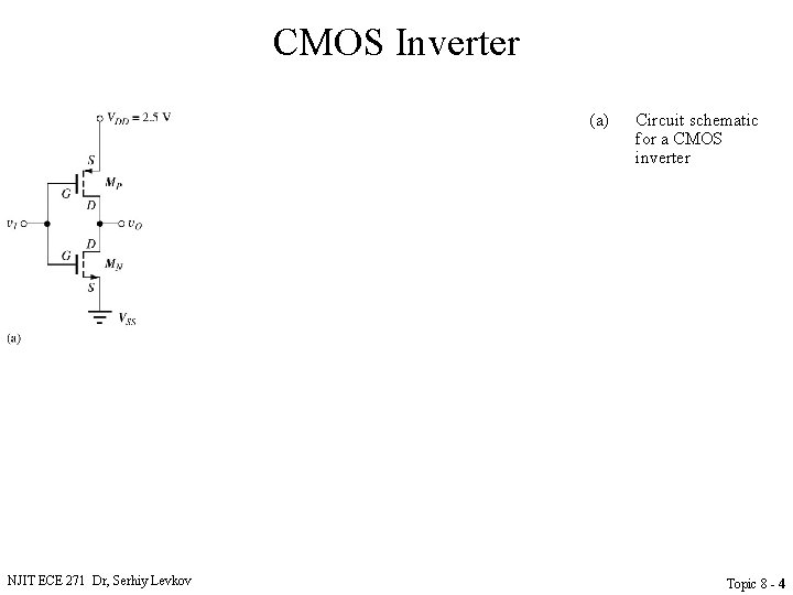
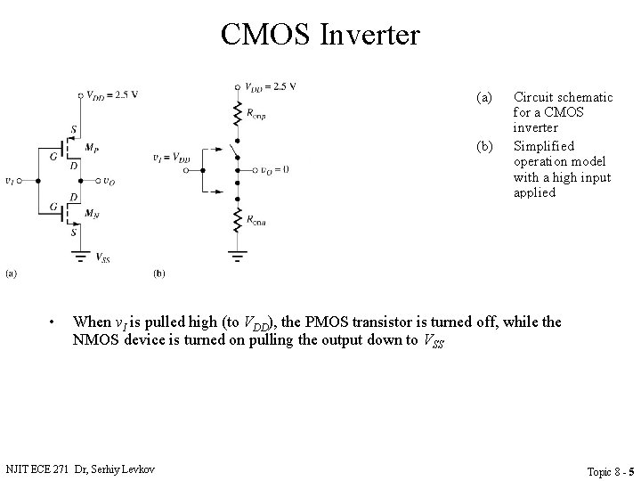
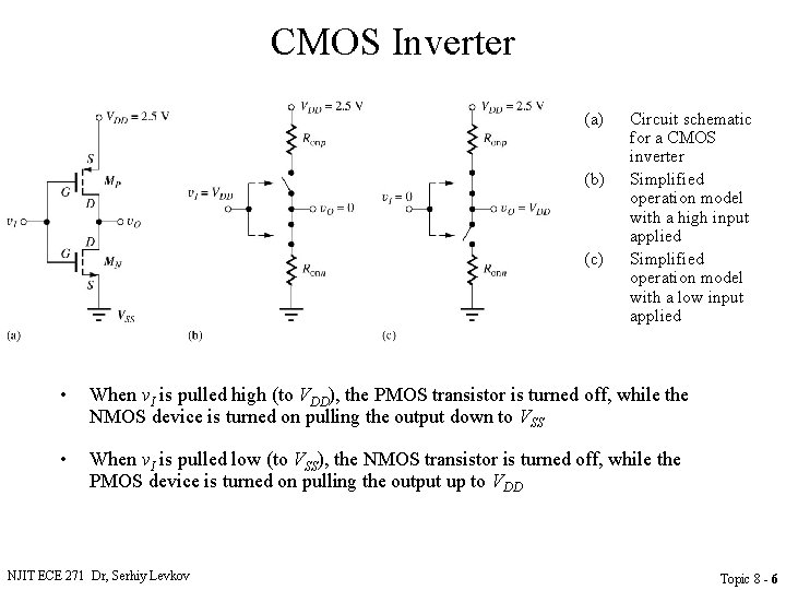
CMOS Inverter (a) (b) (c) NJIT ECE 271 Dr, Serhiy Levkov Circuit schematic for a CMOS inverter Simplified operation model with a high input applied Simplified operation model with a low input applied Topic 8 - 4

CMOS Inverter (a) (b) (c) • Circuit schematic for a CMOS inverter Simplified operation model with a high input applied Simplified operation model with a low input applied When v. I is pulled high (to VDD), the PMOS transistor is turned off, while the NMOS device is turned on pulling the output down to VSS NJIT ECE 271 Dr, Serhiy Levkov Topic 8 - 5

CMOS Inverter (a) (b) (c) Circuit schematic for a CMOS inverter Simplified operation model with a high input applied Simplified operation model with a low input applied • When v. I is pulled high (to VDD), the PMOS transistor is turned off, while the NMOS device is turned on pulling the output down to VSS • When v. I is pulled low (to VSS), the NMOS transistor is turned off, while the PMOS device is turned on pulling the output up to VDD NJIT ECE 271 Dr, Serhiy Levkov Topic 8 - 6

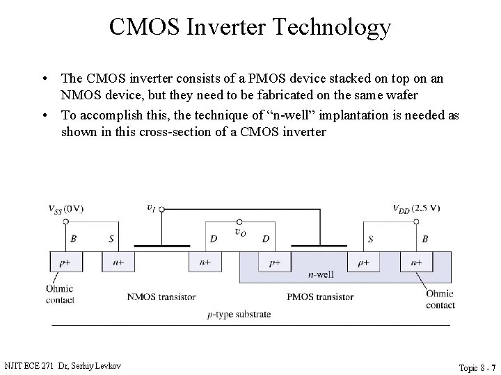
CMOS Inverter Technology • The CMOS inverter consists of a PMOS device stacked on top on an NMOS device, but they need to be fabricated on the same wafer • To accomplish this, the technique of “n-well” implantation is needed as shown in this cross-section of a CMOS inverter NJIT ECE 271 Dr, Serhiy Levkov Topic 8 - 7

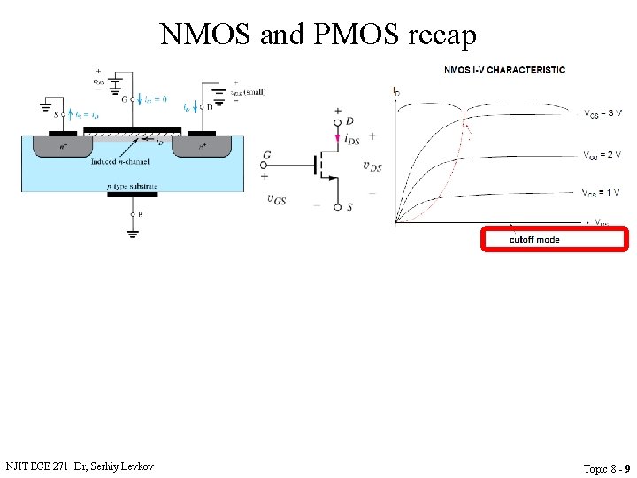
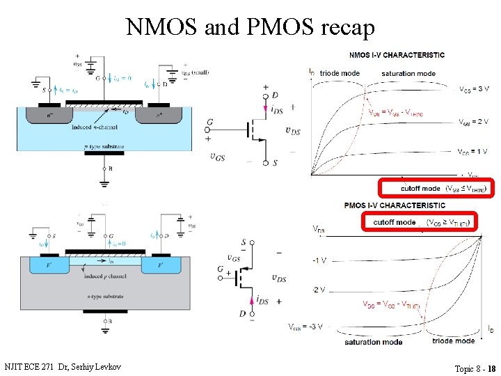
NMOS and PMOS recap NJIT ECE 271 Dr, Serhiy Levkov Topic 8 - 8

NMOS and PMOS recap NJIT ECE 271 Dr, Serhiy Levkov Topic 8 - 9

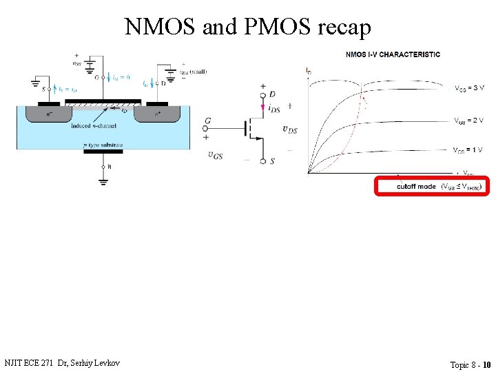
NMOS and PMOS recap NJIT ECE 271 Dr, Serhiy Levkov Topic 8 - 10

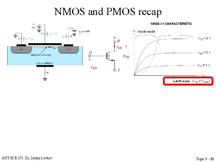
NMOS and PMOS recap NJIT ECE 271 Dr, Serhiy Levkov Topic 8 - 11

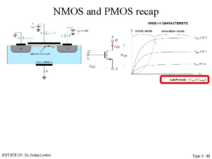
NMOS and PMOS recap NJIT ECE 271 Dr, Serhiy Levkov Topic 8 - 12

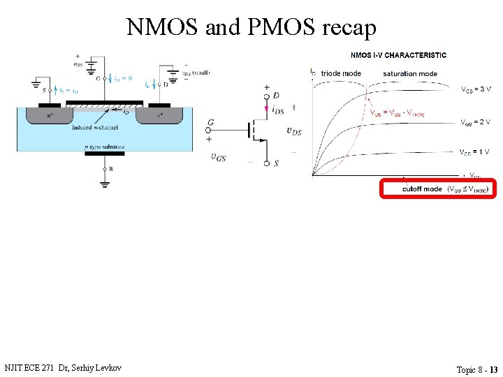
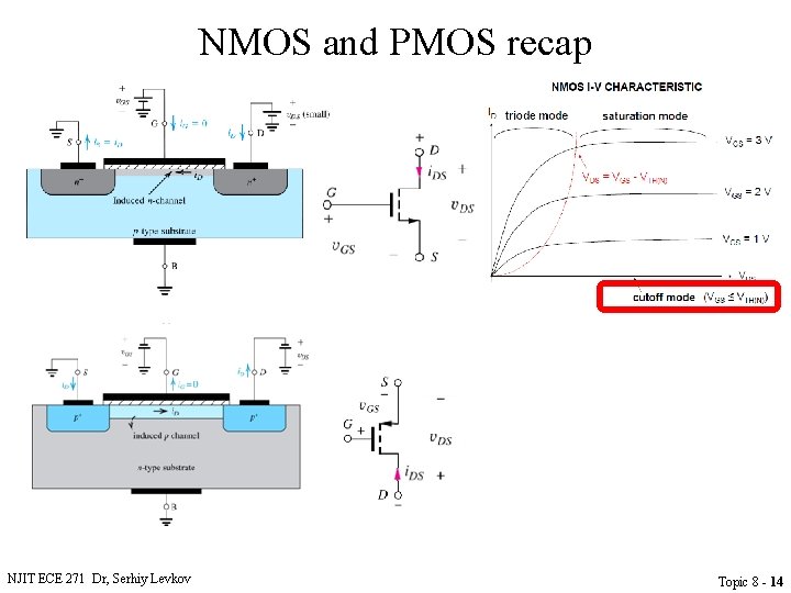
NMOS and PMOS recap NJIT ECE 271 Dr, Serhiy Levkov Topic 8 - 13

NMOS and PMOS recap NJIT ECE 271 Dr, Serhiy Levkov Topic 8 - 14

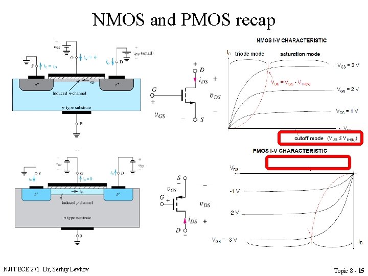
NMOS and PMOS recap NJIT ECE 271 Dr, Serhiy Levkov Topic 8 - 15

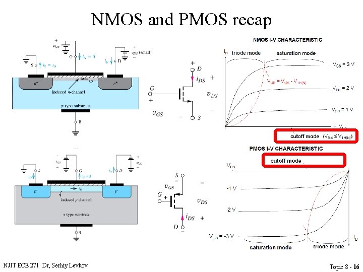
NMOS and PMOS recap NJIT ECE 271 Dr, Serhiy Levkov Topic 8 - 16

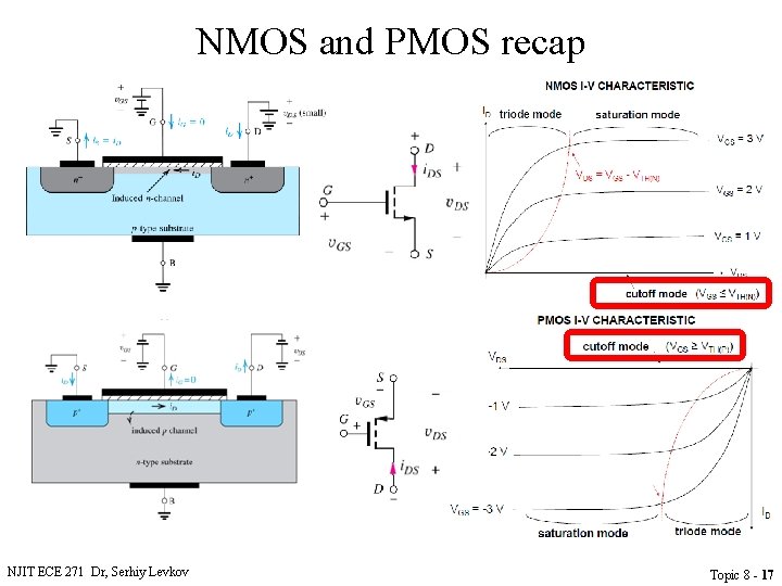
NMOS and PMOS recap NJIT ECE 271 Dr, Serhiy Levkov Topic 8 - 17

NMOS and PMOS recap NJIT ECE 271 Dr, Serhiy Levkov Topic 8 - 18

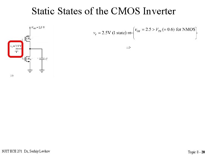
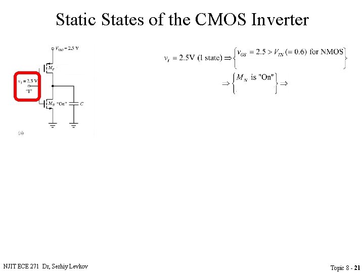
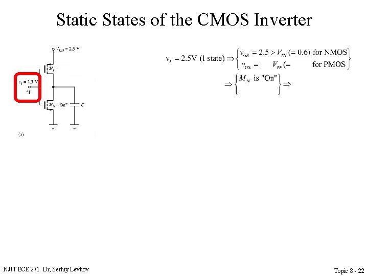
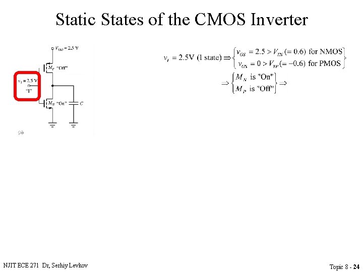
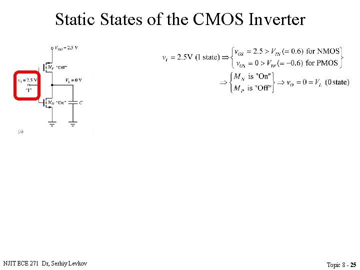
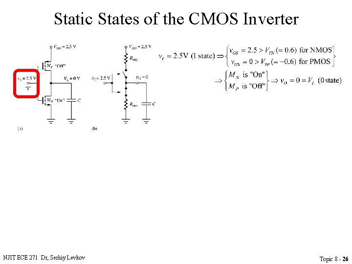
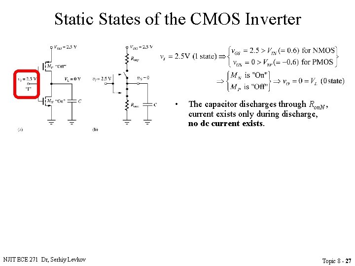
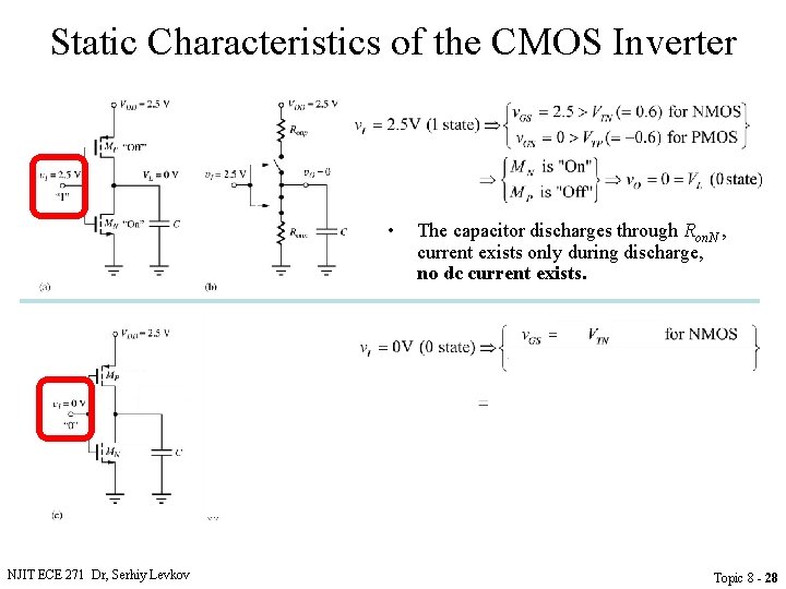
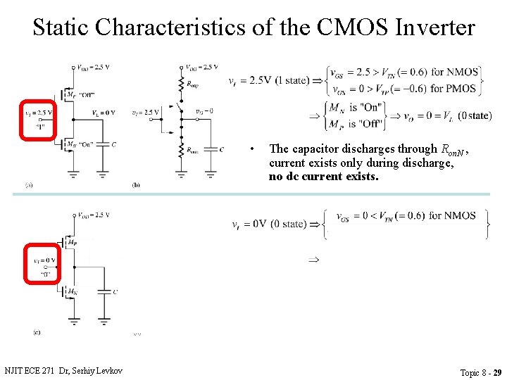
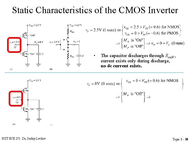
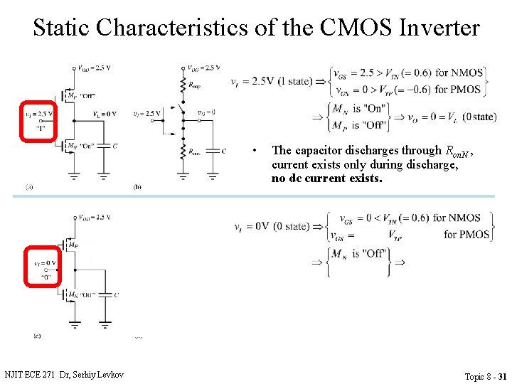
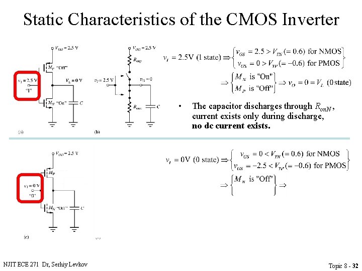
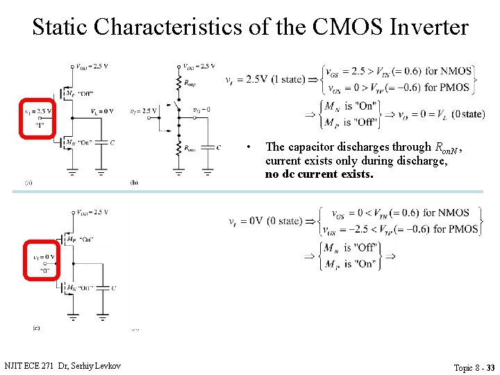
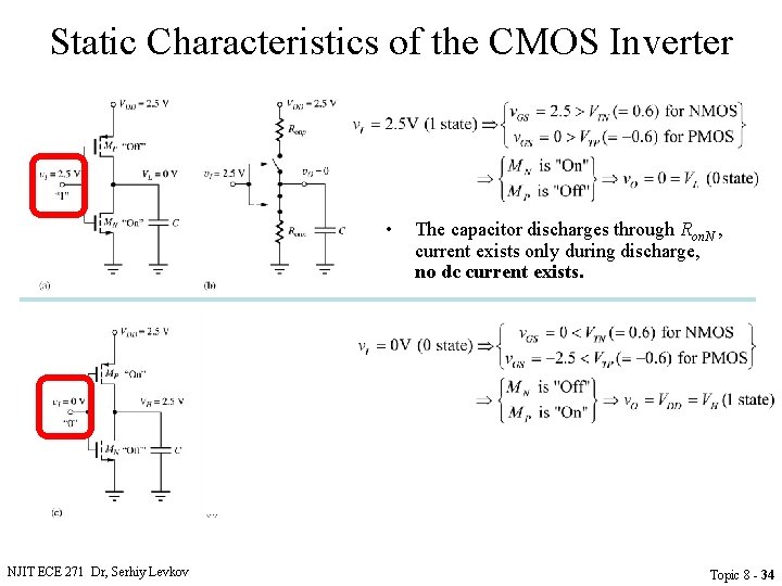
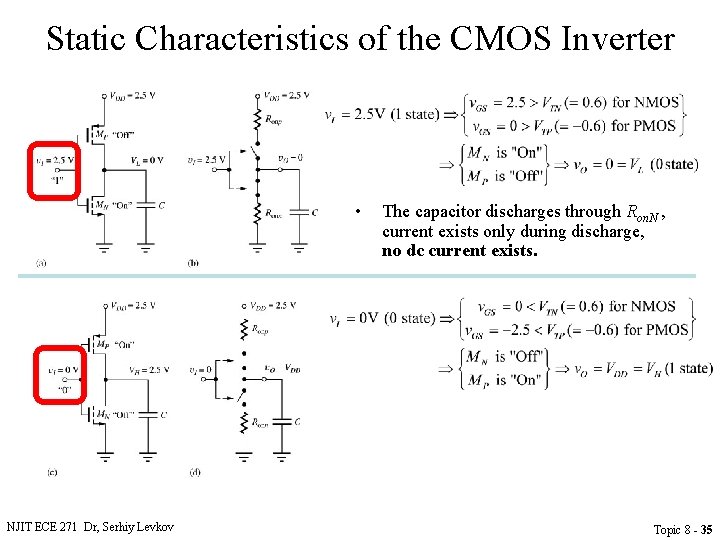
Static States of the CMOS Inverter • NJIT ECE 271 Dr, Serhiy Levkov The capacitor discharges through Ron. N , current exists only during discharge, no dc current exists. Topic 8 - 19

Static States of the CMOS Inverter • NJIT ECE 271 Dr, Serhiy Levkov The capacitor discharges through Ron. N , current exists only during discharge, no dc current exists. Topic 8 - 20

Static States of the CMOS Inverter • NJIT ECE 271 Dr, Serhiy Levkov The capacitor discharges through Ron. N , current exists only during discharge, no dc current exists. Topic 8 - 21

Static States of the CMOS Inverter • NJIT ECE 271 Dr, Serhiy Levkov The capacitor discharges through Ron. N , current exists only during discharge, no dc current exists. Topic 8 - 22

Static States of the CMOS Inverter • NJIT ECE 271 Dr, Serhiy Levkov The capacitor discharges through Ron. N , current exists only during discharge, no dc current exists. Topic 8 - 23

Static States of the CMOS Inverter • NJIT ECE 271 Dr, Serhiy Levkov The capacitor discharges through Ron. N , current exists only during discharge, no dc current exists. Topic 8 - 24

Static States of the CMOS Inverter • NJIT ECE 271 Dr, Serhiy Levkov The capacitor discharges through Ron. N , current exists only during discharge, no dc current exists. Topic 8 - 25

Static States of the CMOS Inverter • NJIT ECE 271 Dr, Serhiy Levkov The capacitor discharges through Ron. N , current exists only during discharge, no dc current exists. Topic 8 - 26

Static States of the CMOS Inverter • NJIT ECE 271 Dr, Serhiy Levkov The capacitor discharges through Ron. N , current exists only during discharge, no dc current exists. Topic 8 - 27

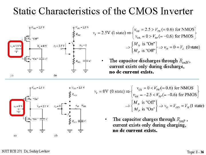
Static Characteristics of the CMOS Inverter • The capacitor discharges through Ron. N , current exists only during discharge, no dc current exists. • NJIT ECE 271 Dr, Serhiy Levkov The capacitor charges through Ron. P , current exists only during charging, no dc current exists. Topic 8 - 28

Static Characteristics of the CMOS Inverter • The capacitor discharges through Ron. N , current exists only during discharge, no dc current exists. • NJIT ECE 271 Dr, Serhiy Levkov The capacitor charges through Ron. P , current exists only during charging, no dc current exists. Topic 8 - 29

Static Characteristics of the CMOS Inverter • The capacitor discharges through Ron. N , current exists only during discharge, no dc current exists. • NJIT ECE 271 Dr, Serhiy Levkov The capacitor charges through Ron. P , current exists only during charging, no dc current exists. Topic 8 - 30

Static Characteristics of the CMOS Inverter • The capacitor discharges through Ron. N , current exists only during discharge, no dc current exists. • NJIT ECE 271 Dr, Serhiy Levkov The capacitor charges through Ron. P , current exists only during charging, no dc current exists. Topic 8 - 31

Static Characteristics of the CMOS Inverter • The capacitor discharges through Ron. N , current exists only during discharge, no dc current exists. • NJIT ECE 271 Dr, Serhiy Levkov The capacitor charges through Ron. P , current exists only during charging, no dc current exists. Topic 8 - 32

Static Characteristics of the CMOS Inverter • The capacitor discharges through Ron. N , current exists only during discharge, no dc current exists. • NJIT ECE 271 Dr, Serhiy Levkov The capacitor charges through Ron. P , current exists only during charging, no dc current exists. Topic 8 - 33

Static Characteristics of the CMOS Inverter • The capacitor discharges through Ron. N , current exists only during discharge, no dc current exists. • NJIT ECE 271 Dr, Serhiy Levkov The capacitor charges through Ron. P , current exists only during charging, no dc current exists. Topic 8 - 34

Static Characteristics of the CMOS Inverter • The capacitor discharges through Ron. N , current exists only during discharge, no dc current exists. • NJIT ECE 271 Dr, Serhiy Levkov The capacitor charges through Ron. P , current exists only during charging, no dc current exists. Topic 8 - 35

Static Characteristics of the CMOS Inverter • The capacitor discharges through Ron. N , current exists only during discharge, no dc current exists. • NJIT ECE 271 Dr, Serhiy Levkov The capacitor charges through Ron. P , current exists only during charging, no dc current exists. Topic 8 - 36

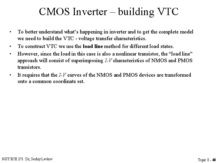
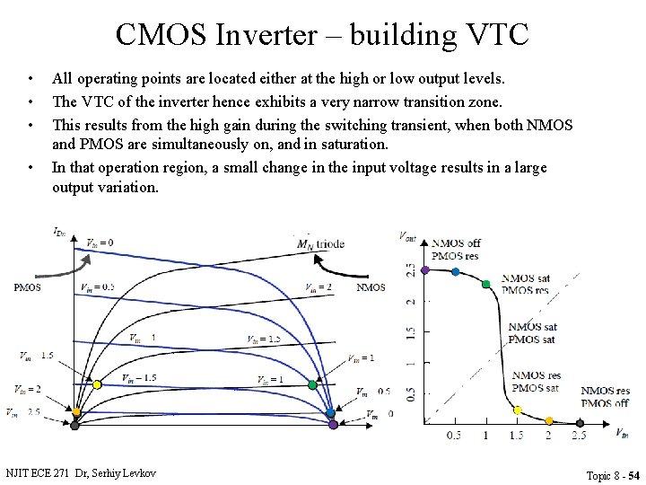
CMOS Inverter – building VTC • To better understand what’s happening in inverter and to get the complete model we need to build the VTC - voltage transfer characteristics. NJIT ECE 271 Dr, Serhiy Levkov Topic 8 - 37

CMOS Inverter – building VTC • • To better understand what’s happening in inverter and to get the complete model we need to build the VTC - voltage transfer characteristics. To construct VTC we use the load line method for different load states. NJIT ECE 271 Dr, Serhiy Levkov Topic 8 - 38

CMOS Inverter – building VTC • • • To better understand what’s happening in inverter and to get the complete model we need to build the VTC - voltage transfer characteristics. To construct VTC we use the load line method for different load states. However, since the load in this case is also a nonlinear transistor, the “load line” approach will consist of superimposing I-V characteristics of NMOS and PMOS transistors. NJIT ECE 271 Dr, Serhiy Levkov Topic 8 - 39

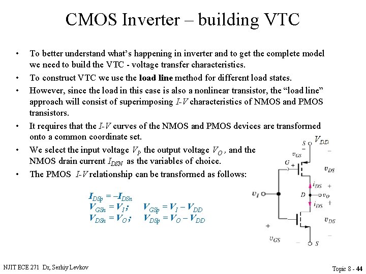
CMOS Inverter – building VTC • • To better understand what’s happening in inverter and to get the complete model we need to build the VTC - voltage transfer characteristics. To construct VTC we use the load line method for different load states. However, since the load in this case is also a nonlinear transistor, the “load line” approach will consist of superimposing I-V characteristics of NMOS and PMOS transistors. It requires that the I-V curves of the NMOS and PMOS devices are transformed onto a common coordinate set. NJIT ECE 271 Dr, Serhiy Levkov Topic 8 - 40

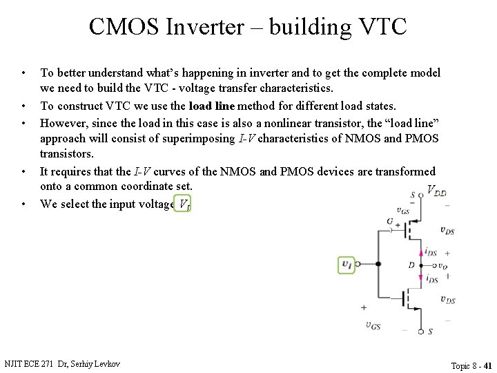
CMOS Inverter – building VTC • • • To better understand what’s happening in inverter and to get the complete model we need to build the VTC - voltage transfer characteristics. To construct VTC we use the load line method for different load states. However, since the load in this case is also a nonlinear transistor, the “load line” approach will consist of superimposing I-V characteristics of NMOS and PMOS transistors. It requires that the I-V curves of the NMOS and PMOS devices are transformed onto a common coordinate set. We select the input voltage VI NJIT ECE 271 Dr, Serhiy Levkov Topic 8 - 41

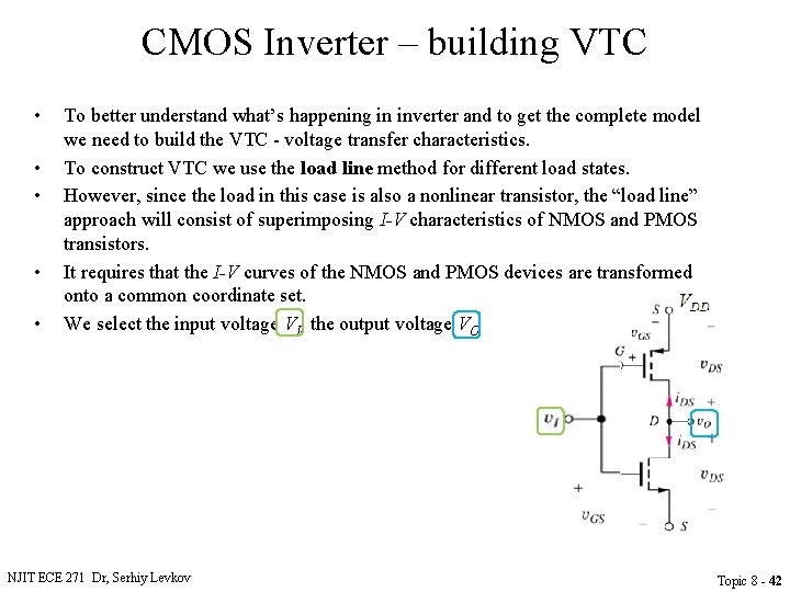
CMOS Inverter – building VTC • • • To better understand what’s happening in inverter and to get the complete model we need to build the VTC - voltage transfer characteristics. To construct VTC we use the load line method for different load states. However, since the load in this case is also a nonlinear transistor, the “load line” approach will consist of superimposing I-V characteristics of NMOS and PMOS transistors. It requires that the I-V curves of the NMOS and PMOS devices are transformed onto a common coordinate set. We select the input voltage VI, the output voltage VO NJIT ECE 271 Dr, Serhiy Levkov Topic 8 - 42

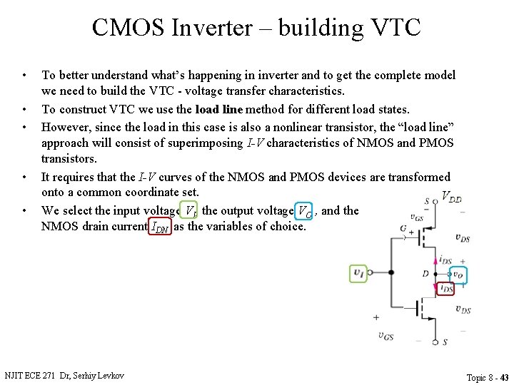
CMOS Inverter – building VTC • • • To better understand what’s happening in inverter and to get the complete model we need to build the VTC - voltage transfer characteristics. To construct VTC we use the load line method for different load states. However, since the load in this case is also a nonlinear transistor, the “load line” approach will consist of superimposing I-V characteristics of NMOS and PMOS transistors. It requires that the I-V curves of the NMOS and PMOS devices are transformed onto a common coordinate set. We select the input voltage VI, the output voltage VO , and the NMOS drain current IDN as the variables of choice. NJIT ECE 271 Dr, Serhiy Levkov Topic 8 - 43

CMOS Inverter – building VTC • • • To better understand what’s happening in inverter and to get the complete model we need to build the VTC - voltage transfer characteristics. To construct VTC we use the load line method for different load states. However, since the load in this case is also a nonlinear transistor, the “load line” approach will consist of superimposing I-V characteristics of NMOS and PMOS transistors. It requires that the I-V curves of the NMOS and PMOS devices are transformed onto a common coordinate set. We select the input voltage VI, the output voltage VO , and the NMOS drain current IDSN as the variables of choice. The PMOS I-V relationship can be transformed as follows: IDSp = –IDSn VGSn = VI ; VDSn = VO ; NJIT ECE 271 Dr, Serhiy Levkov VGSp = VI – VDD VDSp = VO – VDD Topic 8 - 44

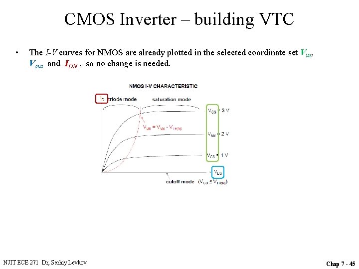
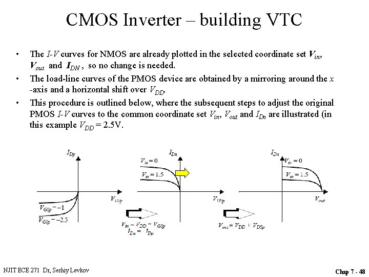
CMOS Inverter – building VTC • The I-V curves for NMOS are already plotted in the selected coordinate set Vin, Vout and IDN , so no change is needed. NJIT ECE 271 Dr, Serhiy Levkov Chap 7 - 45

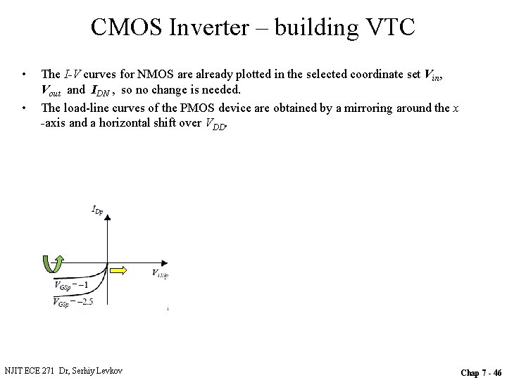
CMOS Inverter – building VTC • • The I-V curves for NMOS are already plotted in the selected coordinate set Vin, Vout and IDN , so no change is needed. The load-line curves of the PMOS device are obtained by a mirroring around the x -axis and a horizontal shift over VDD. NJIT ECE 271 Dr, Serhiy Levkov Chap 7 - 46

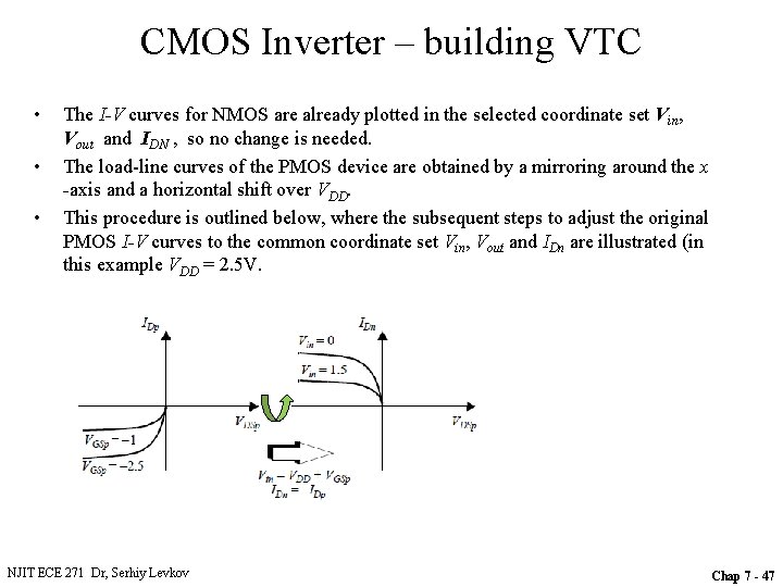
CMOS Inverter – building VTC • • • The I-V curves for NMOS are already plotted in the selected coordinate set Vin, Vout and IDN , so no change is needed. The load-line curves of the PMOS device are obtained by a mirroring around the x -axis and a horizontal shift over VDD. This procedure is outlined below, where the subsequent steps to adjust the original PMOS I-V curves to the common coordinate set Vin, Vout and IDn are illustrated (in this example VDD = 2. 5 V. NJIT ECE 271 Dr, Serhiy Levkov Chap 7 - 47

CMOS Inverter – building VTC • • • The I-V curves for NMOS are already plotted in the selected coordinate set Vin, Vout and IDN , so no change is needed. The load-line curves of the PMOS device are obtained by a mirroring around the x -axis and a horizontal shift over VDD. This procedure is outlined below, where the subsequent steps to adjust the original PMOS I-V curves to the common coordinate set Vin, Vout and IDn are illustrated (in this example VDD = 2. 5 V. NJIT ECE 271 Dr, Serhiy Levkov Chap 7 - 48

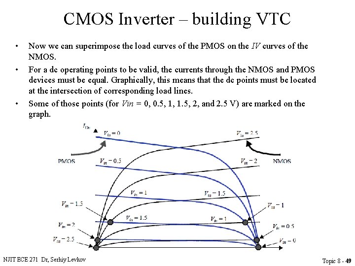
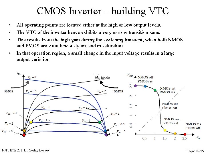
CMOS Inverter – building VTC • • • Now we can superimpose the load curves of the PMOS on the IV curves of the NMOS. For a dc operating points to be valid, the currents through the NMOS and PMOS devices must be equal. Graphically, this means that the dc points must be located at the intersection of corresponding load lines. Some of those points (for Vin = 0, 0. 5, 1, 1. 5, 2, and 2. 5 V) are marked on the graph. NJIT ECE 271 Dr, Serhiy Levkov Topic 8 - 49

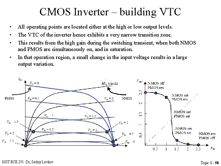
CMOS Inverter – building VTC • • All operating points are located either at the high or low output levels. The VTC of the inverter hence exhibits a very narrow transition zone. This results from the high gain during the switching transient, when both NMOS and PMOS are simultaneously on, and in saturation. In that operation region, a small change in the input voltage results in a large output variation. NJIT ECE 271 Dr, Serhiy Levkov Topic 8 - 50

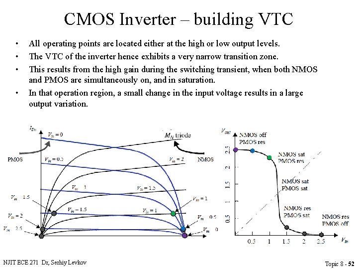
CMOS Inverter – building VTC • • All operating points are located either at the high or low output levels. The VTC of the inverter hence exhibits a very narrow transition zone. This results from the high gain during the switching transient, when both NMOS and PMOS are simultaneously on, and in saturation. In that operation region, a small change in the input voltage results in a large output variation. NJIT ECE 271 Dr, Serhiy Levkov Topic 8 - 51

CMOS Inverter – building VTC • • All operating points are located either at the high or low output levels. The VTC of the inverter hence exhibits a very narrow transition zone. This results from the high gain during the switching transient, when both NMOS and PMOS are simultaneously on, and in saturation. In that operation region, a small change in the input voltage results in a large output variation. NJIT ECE 271 Dr, Serhiy Levkov Topic 8 - 52

CMOS Inverter – building VTC • • All operating points are located either at the high or low output levels. The VTC of the inverter hence exhibits a very narrow transition zone. This results from the high gain during the switching transient, when both NMOS and PMOS are simultaneously on, and in saturation. In that operation region, a small change in the input voltage results in a large output variation. NJIT ECE 271 Dr, Serhiy Levkov Topic 8 - 53

CMOS Inverter – building VTC • • All operating points are located either at the high or low output levels. The VTC of the inverter hence exhibits a very narrow transition zone. This results from the high gain during the switching transient, when both NMOS and PMOS are simultaneously on, and in saturation. In that operation region, a small change in the input voltage results in a large output variation. NJIT ECE 271 Dr, Serhiy Levkov Topic 8 - 54

CMOS Inverter – building VTC • • All operating points are located either at the high or low output levels. The VTC of the inverter hence exhibits a very narrow transition zone. This results from the high gain during the switching transient, when both NMOS and PMOS are simultaneously on, and in saturation. In that operation region, a small change in the input voltage results in a large output variation. NJIT ECE 271 Dr, Serhiy Levkov Topic 8 - 55

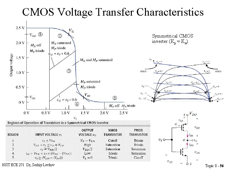
CMOS Voltage Transfer Characteristics Symmetrical CMOS inverter (Kp = Kn). NJIT ECE 271 Dr, Serhiy Levkov Topic 8 - 56

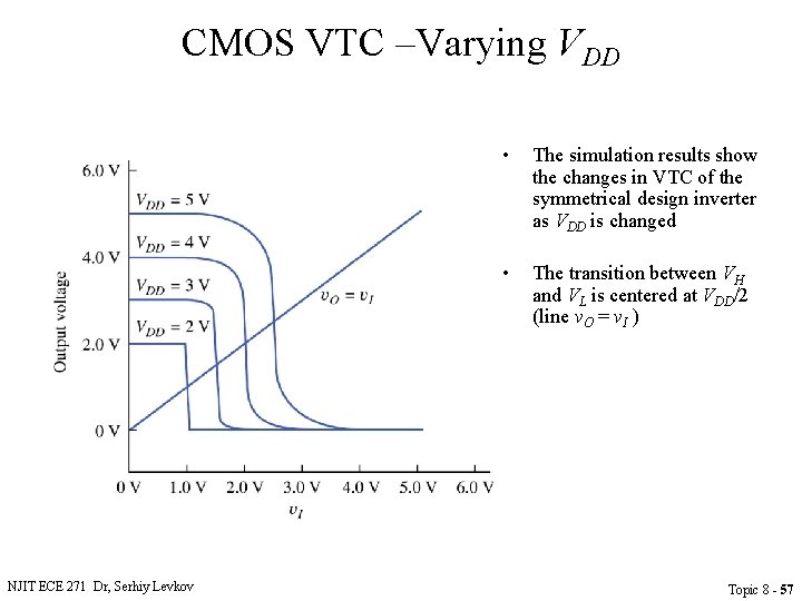
CMOS VTC –Varying VDD NJIT ECE 271 Dr, Serhiy Levkov • The simulation results show the changes in VTC of the symmetrical design inverter as VDD is changed • The transition between VH and VL is centered at VDD/2 (line v. O = v. I ) Topic 8 - 57

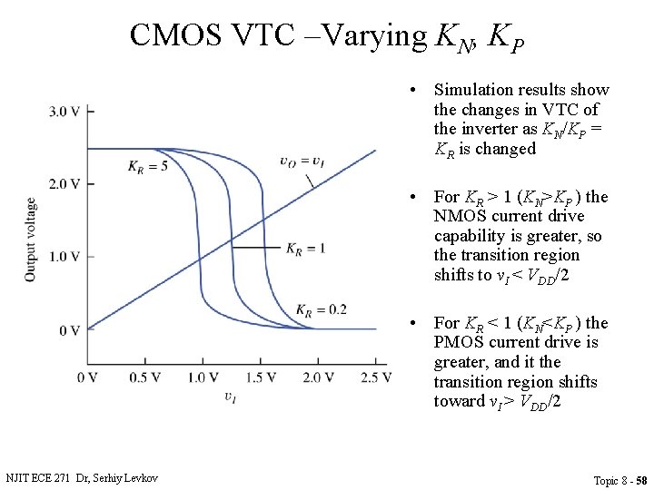
CMOS VTC –Varying KN, KP • Simulation results show the changes in VTC of the inverter as KN/KP = KR is changed • For KR > 1 (KN>KP ) the NMOS current drive capability is greater, so the transition region shifts to v. I < VDD/2 • For KR < 1 (KN<KP ) the PMOS current drive is greater, and it the transition region shifts toward v. I > VDD/2 NJIT ECE 271 Dr, Serhiy Levkov Topic 8 - 58

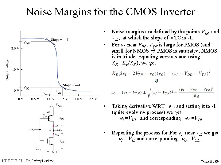
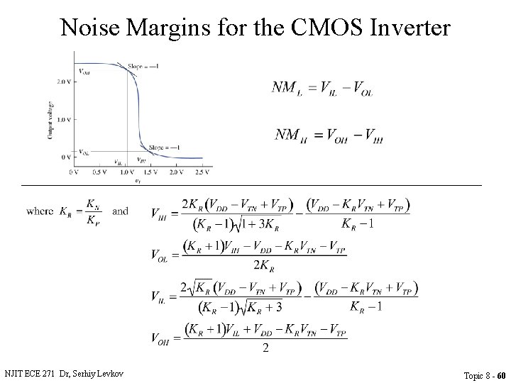
Noise Margins for the CMOS Inverter • • NJIT ECE 271 Dr, Serhiy Levkov Noise margins are defined by the points VIH and VIL, at which the slope of VTC is -1. For v. I near VIH , VDS is large for PMOS (and small for NMOS PMOS is saturated, NMOS is in triode. Equating currents and using KR =KN/KP ), we get • Taking derivative WRT v. I , and setting it to -1 (quite evolving process) we get v. I =VIH and corresponding v. O =VOL • Repeating the process for For v. I near VIL we get v. I = VIL and corresponding v. O =VOL Topic 8 - 59

Noise Margins for the CMOS Inverter NJIT ECE 271 Dr, Serhiy Levkov Topic 8 - 60

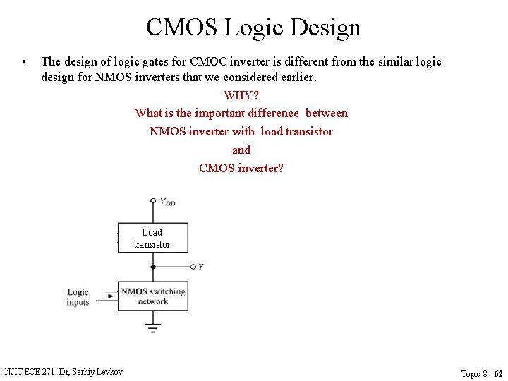
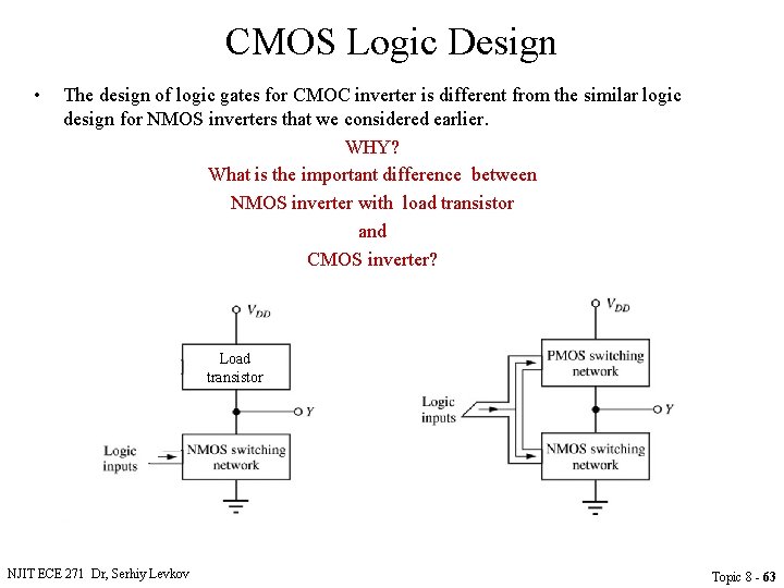
CMOS Logic Design • The design of logic gates for CMOC inverter is different from the similar logic design for NMOS inverters that we considered earlier. WHY? What is the important difference between NMOS inverter with load transistor and CMOS inverter? NJIT ECE 271 Dr, Serhiy Levkov Topic 8 - 61

CMOS Logic Design • The design of logic gates for CMOC inverter is different from the similar logic design for NMOS inverters that we considered earlier. WHY? What is the important difference between NMOS inverter with load transistor and CMOS inverter? Load transistor NJIT ECE 271 Dr, Serhiy Levkov Topic 8 - 62

CMOS Logic Design • The design of logic gates for CMOC inverter is different from the similar logic design for NMOS inverters that we considered earlier. WHY? What is the important difference between NMOS inverter with load transistor and CMOS inverter? Load transistor NJIT ECE 271 Dr, Serhiy Levkov Topic 8 - 63

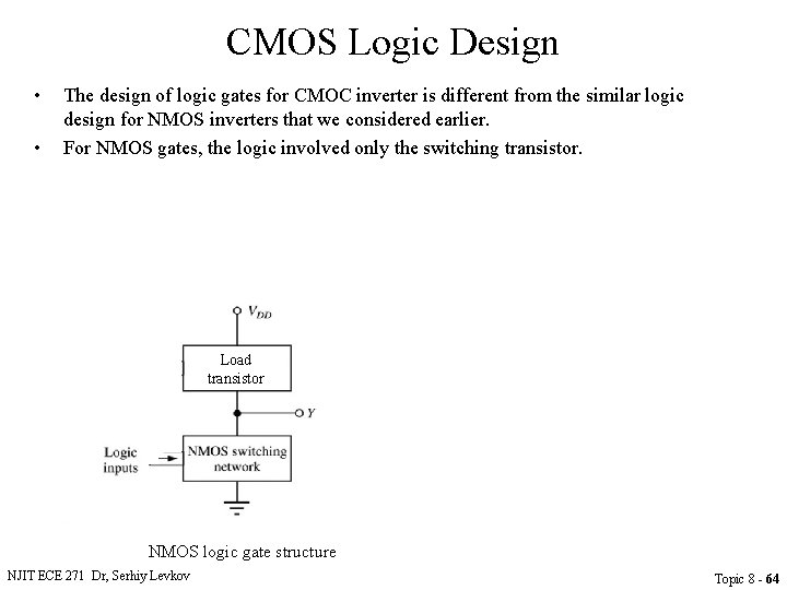
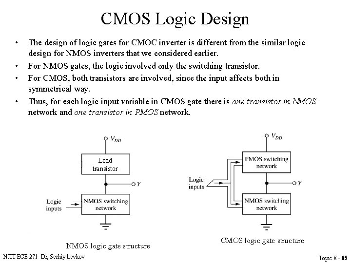
CMOS Logic Design • • The design of logic gates for CMOC inverter is different from the similar logic design for NMOS inverters that we considered earlier. For NMOS gates, the logic involved only the switching transistor. Load transistor NMOS logic gate structure NJIT ECE 271 Dr, Serhiy Levkov Topic 8 - 64

CMOS Logic Design • • The design of logic gates for CMOC inverter is different from the similar logic design for NMOS inverters that we considered earlier. For NMOS gates, the logic involved only the switching transistor. For CMOS, both transistors are involved, since the input affects both in symmetrical way. Thus, for each logic input variable in CMOS gate there is one transistor in NMOS network and one transistor in PMOS network. Load transistor NMOS logic gate structure NJIT ECE 271 Dr, Serhiy Levkov CMOS logic gate structure Topic 8 - 65

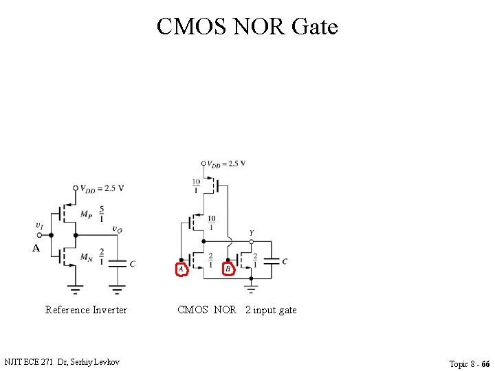
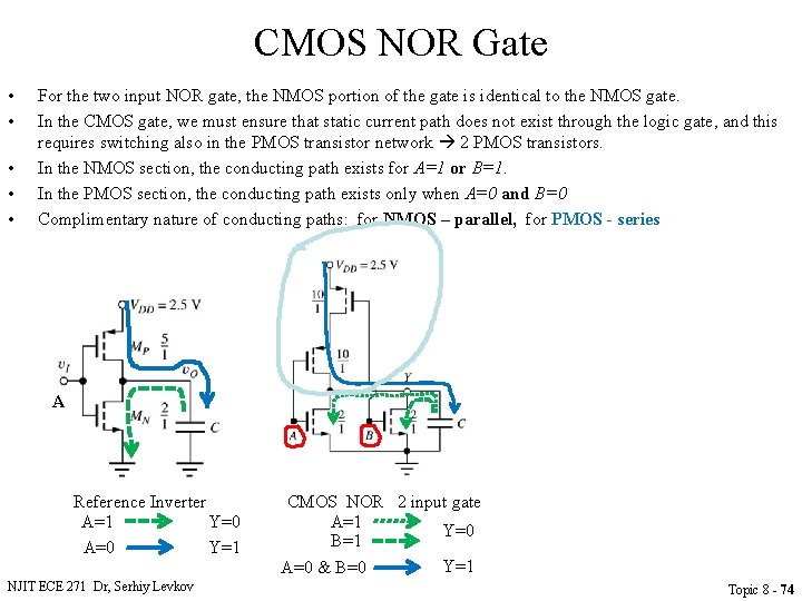
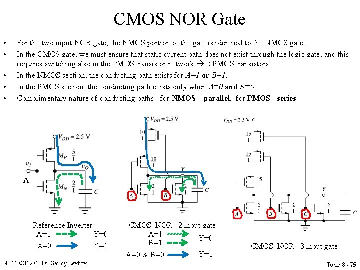
CMOS NOR Gate A Reference Inverter NJIT ECE 271 Dr, Serhiy Levkov CMOS NOR 2 input gate Topic 8 - 66

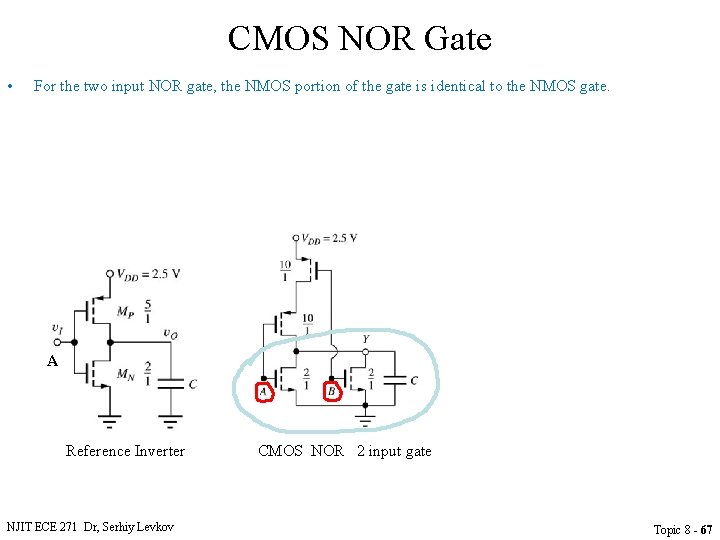
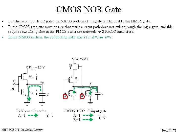
CMOS NOR Gate • For the two input NOR gate, the NMOS portion of the gate is identical to the NMOS gate. A Reference Inverter NJIT ECE 271 Dr, Serhiy Levkov CMOS NOR 2 input gate Topic 8 - 67

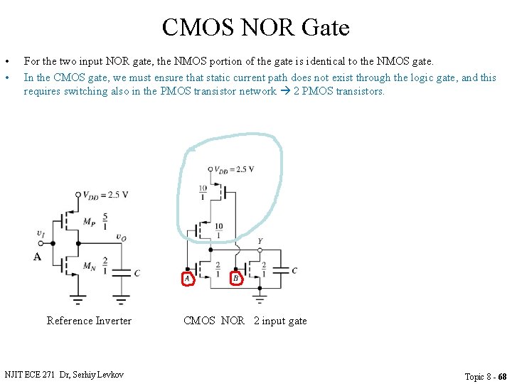
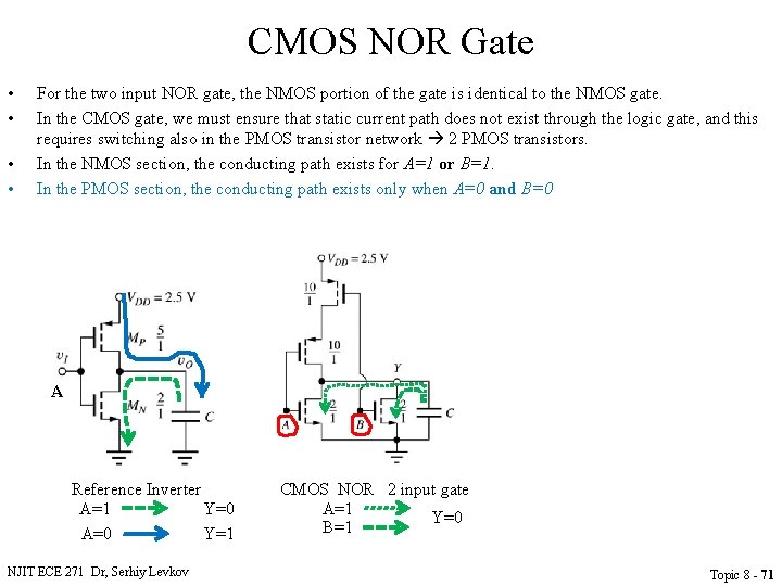
CMOS NOR Gate • • For the two input NOR gate, the NMOS portion of the gate is identical to the NMOS gate. In the CMOS gate, we must ensure that static current path does not exist through the logic gate, and this requires switching also in the PMOS transistor network 2 PMOS transistors. A Reference Inverter NJIT ECE 271 Dr, Serhiy Levkov CMOS NOR 2 input gate Topic 8 - 68

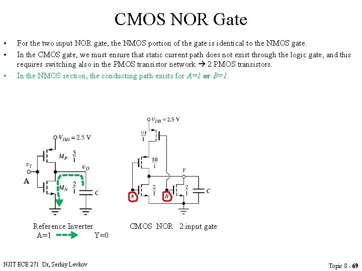
CMOS NOR Gate • • • For the two input NOR gate, the NMOS portion of the gate is identical to the NMOS gate. In the CMOS gate, we must ensure that static current path does not exist through the logic gate, and this requires switching also in the PMOS transistor network 2 PMOS transistors. In the NMOS section, the conducting path exists for A=1 or B=1. A Reference Inverter A=1 Y=0 NJIT ECE 271 Dr, Serhiy Levkov CMOS NOR 2 input gate Topic 8 - 69

CMOS NOR Gate • • • For the two input NOR gate, the NMOS portion of the gate is identical to the NMOS gate. In the CMOS gate, we must ensure that static current path does not exist through the logic gate, and this requires switching also in the PMOS transistor network 2 PMOS transistors. In the NMOS section, the conducting path exists for A=1 or B=1. A Reference Inverter A=1 Y=0 NJIT ECE 271 Dr, Serhiy Levkov CMOS NOR 2 input gate A=1 Y=0 B=1 Topic 8 - 70

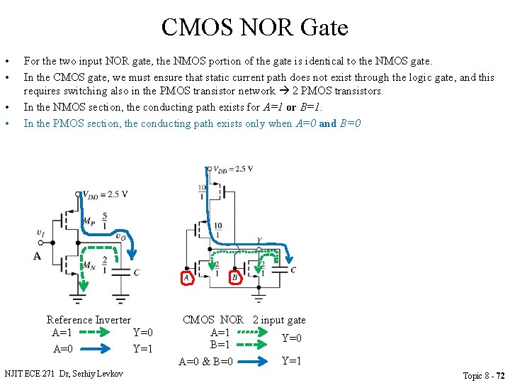
CMOS NOR Gate • • For the two input NOR gate, the NMOS portion of the gate is identical to the NMOS gate. In the CMOS gate, we must ensure that static current path does not exist through the logic gate, and this requires switching also in the PMOS transistor network 2 PMOS transistors. In the NMOS section, the conducting path exists for A=1 or B=1. In the PMOS section, the conducting path exists only when A=0 and B=0 A Reference Inverter A=1 Y=0 A=0 Y=1 NJIT ECE 271 Dr, Serhiy Levkov CMOS NOR 2 input gate A=1 Y=0 B=1 Topic 8 - 71

CMOS NOR Gate • • For the two input NOR gate, the NMOS portion of the gate is identical to the NMOS gate. In the CMOS gate, we must ensure that static current path does not exist through the logic gate, and this requires switching also in the PMOS transistor network 2 PMOS transistors. In the NMOS section, the conducting path exists for A=1 or B=1. In the PMOS section, the conducting path exists only when A=0 and B=0 A Reference Inverter A=1 Y=0 A=0 Y=1 NJIT ECE 271 Dr, Serhiy Levkov CMOS NOR 2 input gate A=1 Y=0 B=1 Y=1 A=0 & B=0 Topic 8 - 72

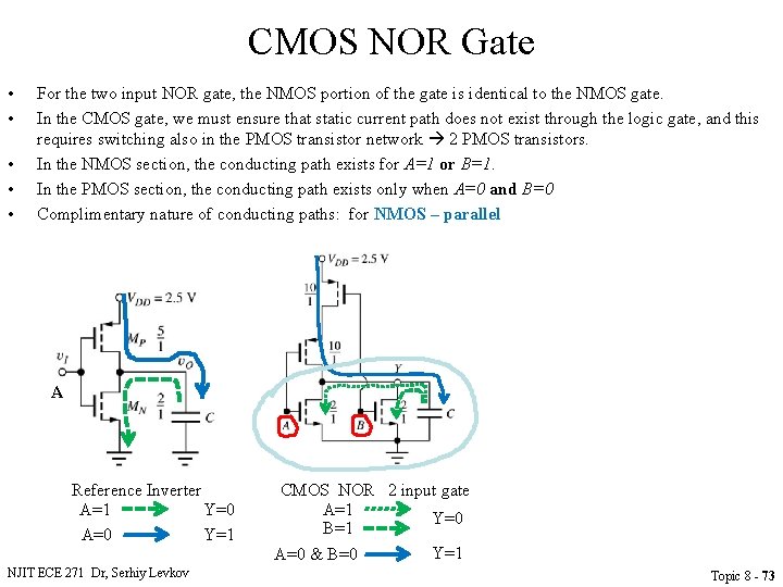
CMOS NOR Gate • • • For the two input NOR gate, the NMOS portion of the gate is identical to the NMOS gate. In the CMOS gate, we must ensure that static current path does not exist through the logic gate, and this requires switching also in the PMOS transistor network 2 PMOS transistors. In the NMOS section, the conducting path exists for A=1 or B=1. In the PMOS section, the conducting path exists only when A=0 and B=0 Complimentary nature of conducting paths: for NMOS – parallel A Reference Inverter A=1 Y=0 A=0 Y=1 NJIT ECE 271 Dr, Serhiy Levkov CMOS NOR 2 input gate A=1 Y=0 B=1 Y=1 A=0 & B=0 Topic 8 - 73

CMOS NOR Gate • • • For the two input NOR gate, the NMOS portion of the gate is identical to the NMOS gate. In the CMOS gate, we must ensure that static current path does not exist through the logic gate, and this requires switching also in the PMOS transistor network 2 PMOS transistors. In the NMOS section, the conducting path exists for A=1 or B=1. In the PMOS section, the conducting path exists only when A=0 and B=0 Complimentary nature of conducting paths: for NMOS – parallel, for PMOS - series A Reference Inverter A=1 Y=0 A=0 Y=1 NJIT ECE 271 Dr, Serhiy Levkov CMOS NOR 2 input gate A=1 Y=0 B=1 Y=1 A=0 & B=0 Topic 8 - 74

CMOS NOR Gate • • • For the two input NOR gate, the NMOS portion of the gate is identical to the NMOS gate. In the CMOS gate, we must ensure that static current path does not exist through the logic gate, and this requires switching also in the PMOS transistor network 2 PMOS transistors. In the NMOS section, the conducting path exists for A=1 or B=1. In the PMOS section, the conducting path exists only when A=0 and B=0 Complimentary nature of conducting paths: for NMOS – parallel, for PMOS - series A Reference Inverter A=1 Y=0 A=0 Y=1 NJIT ECE 271 Dr, Serhiy Levkov CMOS NOR 2 input gate A=1 Y=0 B=1 Y=1 A=0 & B=0 CMOS NOR 3 input gate Topic 8 - 75

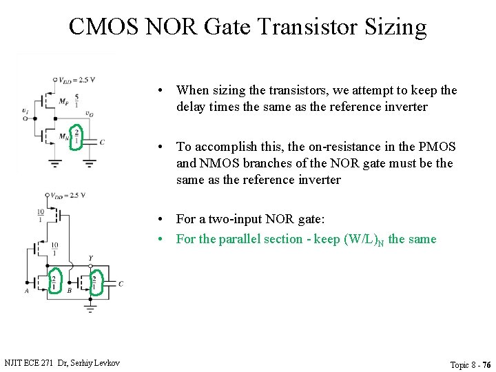
CMOS NOR Gate Transistor Sizing • When sizing the transistors, we attempt to keep the delay times the same as the reference inverter • To accomplish this, the on-resistance in the PMOS and NMOS branches of the NOR gate must be the same as the reference inverter • For a two-input NOR gate: • For the parallel section - keep (W/L)N the same NJIT ECE 271 Dr, Serhiy Levkov Topic 8 - 76

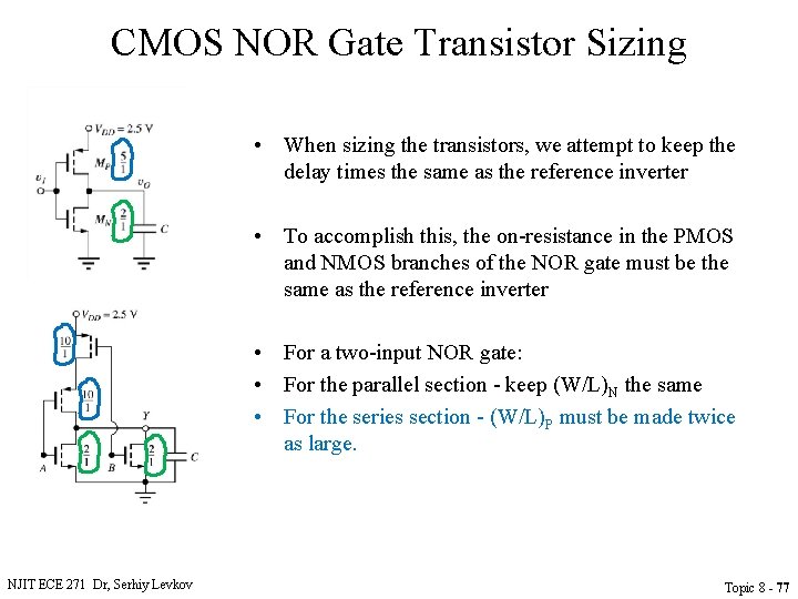
CMOS NOR Gate Transistor Sizing • When sizing the transistors, we attempt to keep the delay times the same as the reference inverter • To accomplish this, the on-resistance in the PMOS and NMOS branches of the NOR gate must be the same as the reference inverter • For a two-input NOR gate: • For the parallel section - keep (W/L)N the same • For the series section - (W/L)P must be made twice as large. NJIT ECE 271 Dr, Serhiy Levkov Topic 8 - 77

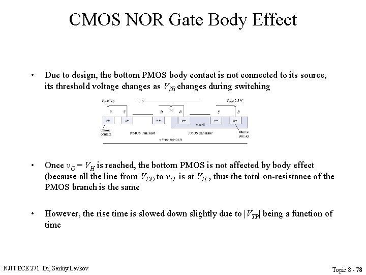
CMOS NOR Gate Body Effect • Due to design, the bottom PMOS body contact is not connected to its source, its threshold voltage changes as VSB changes during switching • Once v. O = VH is reached, the bottom PMOS is not affected by body effect (because all the line from VDD to v. O is at VH , thus the total on-resistance of the PMOS branch is the same • However, the rise time is slowed down slightly due to |VTP| being a function of time NJIT ECE 271 Dr, Serhiy Levkov Topic 8 - 78

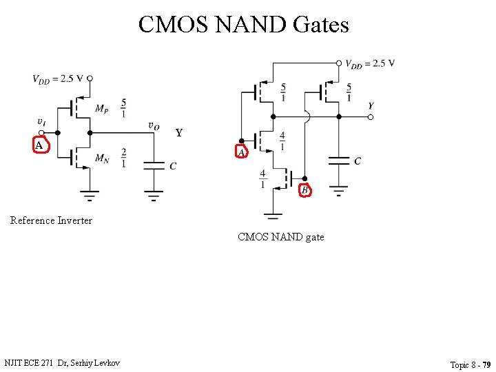
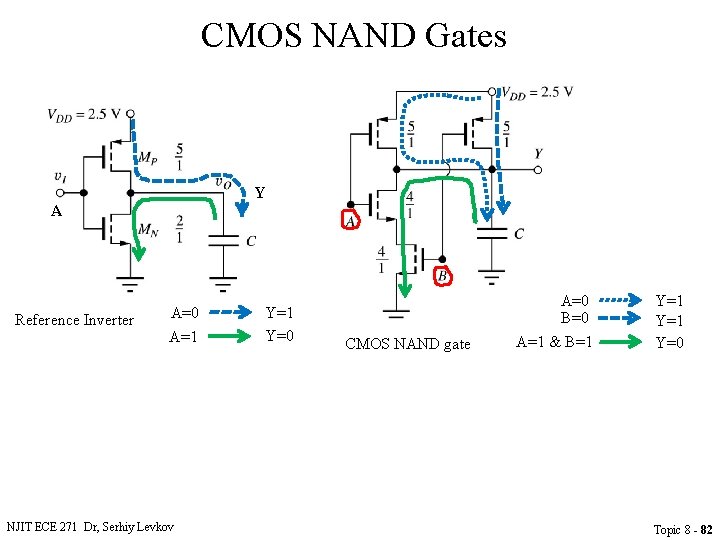
CMOS NAND Gates Y A Reference Inverter CMOS NAND gate NJIT ECE 271 Dr, Serhiy Levkov Topic 8 - 79

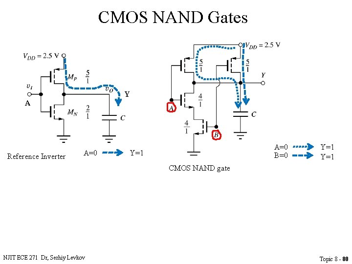
CMOS NAND Gates Y A Reference Inverter A=0 B=0 Y=1 Y=1 CMOS NAND gate NJIT ECE 271 Dr, Serhiy Levkov Topic 8 - 80

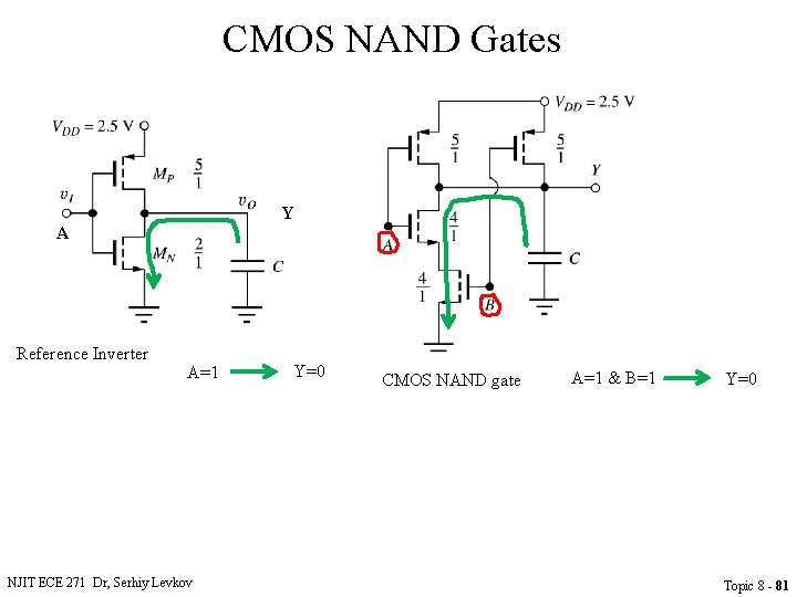
CMOS NAND Gates Y A Reference Inverter A=1 NJIT ECE 271 Dr, Serhiy Levkov Y=0 CMOS NAND gate A=1 & B=1 Y=0 Topic 8 - 81

CMOS NAND Gates Y A Reference Inverter A=0 A=1 NJIT ECE 271 Dr, Serhiy Levkov Y=1 Y=0 CMOS NAND gate A=0 B=0 A=1 & B=1 Y=1 Y=0 Topic 8 - 82

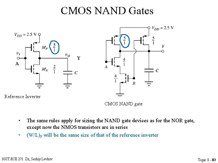
CMOS NAND Gates Y A Reference Inverter CMOS NAND gate • • The same rules apply for sizing the NAND gate devices as for the NOR gate, except now the NMOS transistors are in series (W/L)P will be the same size of that of the reference inverter NJIT ECE 271 Dr, Serhiy Levkov Topic 8 - 83

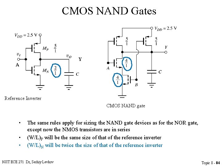
CMOS NAND Gates Y A Reference Inverter CMOS NAND gate • • • The same rules apply for sizing the NAND gate devices as for the NOR gate, except now the NMOS transistors are in series (W/L)P will be the same size of that of the reference inverter (W/L)N will be twice the size of that of the reference inverter NJIT ECE 271 Dr, Serhiy Levkov Topic 8 - 84

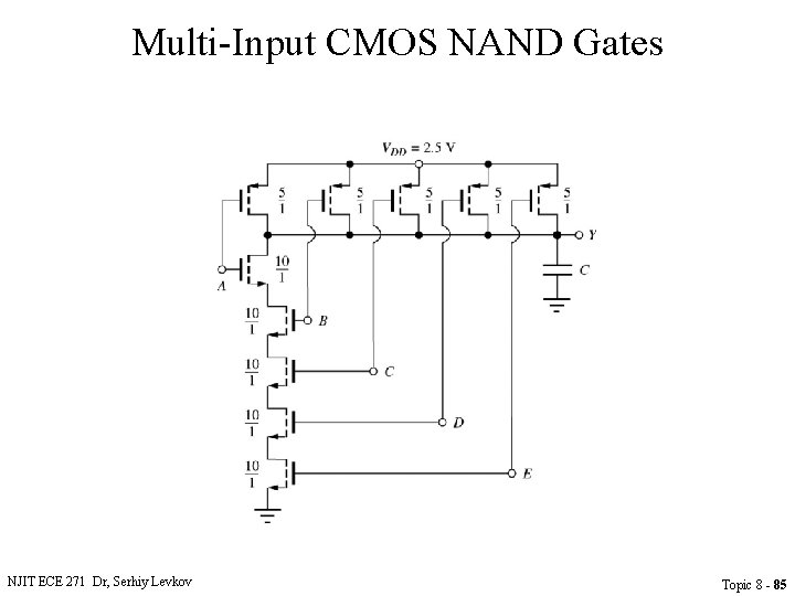
Multi-Input CMOS NAND Gates NJIT ECE 271 Dr, Serhiy Levkov Topic 8 - 85

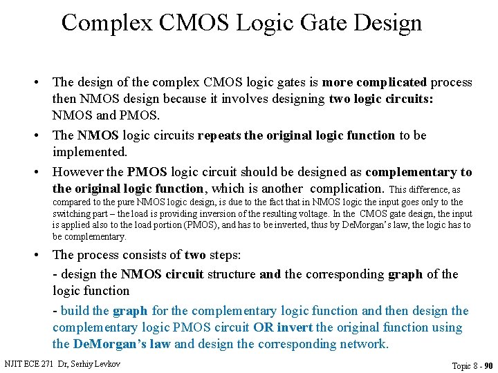
Complex CMOS Logic Gate Design • The design of the complex CMOS logic gates is more complicated process then NMOS design because it involves designing two logic circuits: NMOS and PMOS. NJIT ECE 271 Dr, Serhiy Levkov Topic 8 - 86

Complex CMOS Logic Gate Design • The design of the complex CMOS logic gates is more complicated process then NMOS design because it involves designing two logic circuits: NMOS and PMOS. • The NMOS logic circuits repeats the original logic function to be implemented. NJIT ECE 271 Dr, Serhiy Levkov Topic 8 - 87

Complex CMOS Logic Gate Design • The design of the complex CMOS logic gates is more complicated process then NMOS design because it involves designing two logic circuits: NMOS and PMOS. • The NMOS logic circuits repeats the original logic function to be implemented. • However the PMOS logic circuit should be designed as complementary to the original logic function, which is another complication. This difference, as compared to the pure NMOS logic design, is due to the fact that in NMOS logic the input goes only to the switching part – the load is providing inversion of the resulting voltage. In the CMOS gate design, the input is applied also to the load portion (PMOS), and has to be inverted, thus by De. Morgan’s law, the logic has to be complementary. NJIT ECE 271 Dr, Serhiy Levkov Topic 8 - 88

Complex CMOS Logic Gate Design • The design of the complex CMOS logic gates is more complicated process then NMOS design because it involves designing two logic circuits: NMOS and PMOS. • The NMOS logic circuits repeats the original logic function to be implemented. • However the PMOS logic circuit should be designed as complementary to the original logic function, which is another complication. This difference, as compared to the pure NMOS logic design, is due to the fact that in NMOS logic the input goes only to the switching part – the load is providing inversion of the resulting voltage. In the CMOS gate design, the input is applied also to the load portion (PMOS), and has to be inverted, thus by De. Morgan’s law, the logic has to be complementary. • The process consists of two steps: - design the NMOS circuit structure and the corresponding graph of the logic function NJIT ECE 271 Dr, Serhiy Levkov Topic 8 - 89

Complex CMOS Logic Gate Design • The design of the complex CMOS logic gates is more complicated process then NMOS design because it involves designing two logic circuits: NMOS and PMOS. • The NMOS logic circuits repeats the original logic function to be implemented. • However the PMOS logic circuit should be designed as complementary to the original logic function, which is another complication. This difference, as compared to the pure NMOS logic design, is due to the fact that in NMOS logic the input goes only to the switching part – the load is providing inversion of the resulting voltage. In the CMOS gate design, the input is applied also to the load portion (PMOS), and has to be inverted, thus by De. Morgan’s law, the logic has to be complementary. • The process consists of two steps: - design the NMOS circuit structure and the corresponding graph of the logic function - build the graph for the complementary logic function and then design the complementary logic PMOS circuit OR invert the original function using the De. Morgan’s law and design the corresponding network. NJIT ECE 271 Dr, Serhiy Levkov Topic 8 - 90

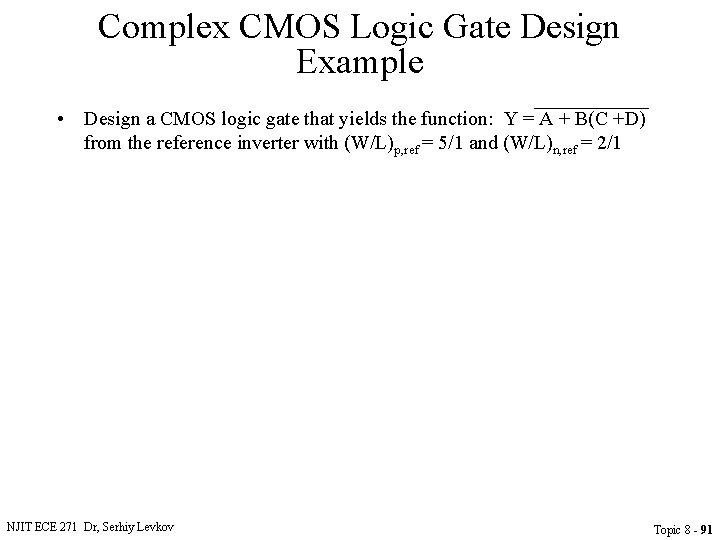
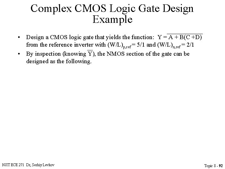
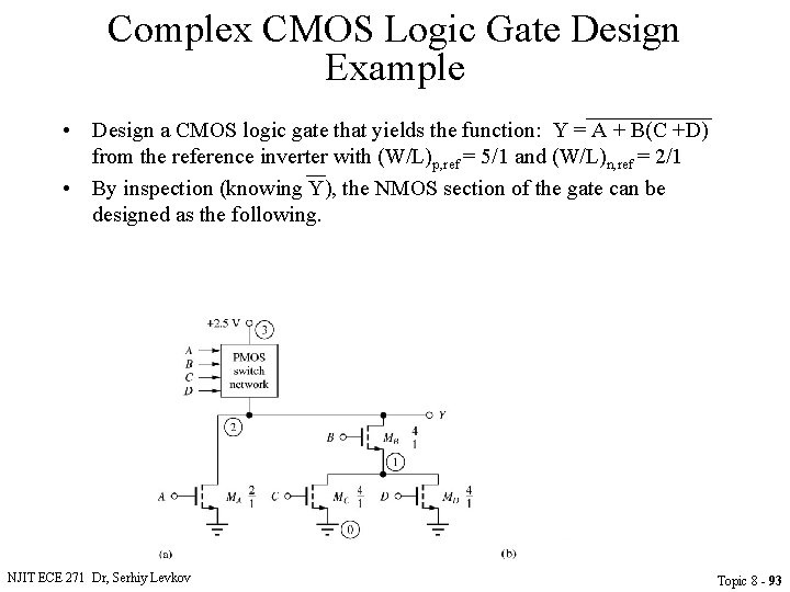
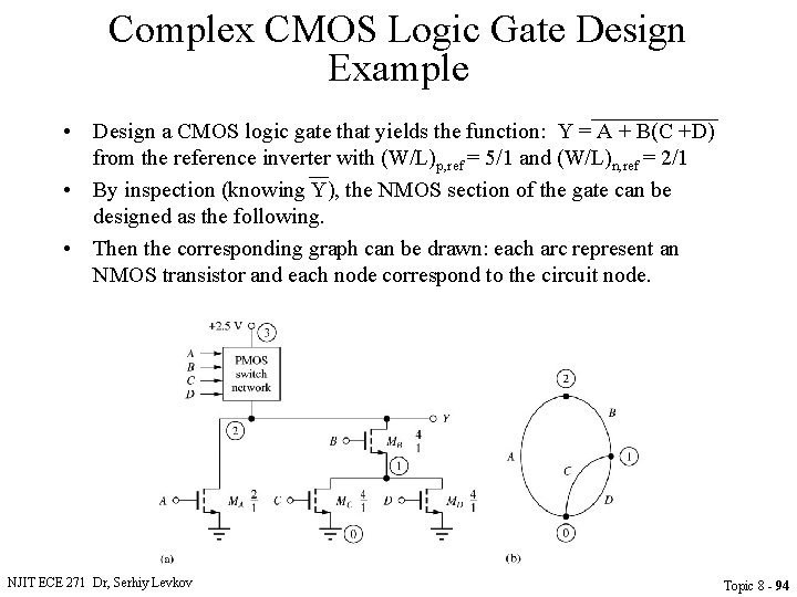
Complex CMOS Logic Gate Design Example • Design a CMOS logic gate that yields the function: Y = A + B(C +D) from the reference inverter with (W/L)p, ref = 5/1 and (W/L)n, ref = 2/1 NJIT ECE 271 Dr, Serhiy Levkov Topic 8 - 91

Complex CMOS Logic Gate Design Example • Design a CMOS logic gate that yields the function: Y = A + B(C +D) from the reference inverter with (W/L)p, ref = 5/1 and (W/L)n, ref = 2/1 • By inspection (knowing Y), the NMOS section of the gate can be designed as the following. NJIT ECE 271 Dr, Serhiy Levkov Topic 8 - 92

Complex CMOS Logic Gate Design Example • Design a CMOS logic gate that yields the function: Y = A + B(C +D) from the reference inverter with (W/L)p, ref = 5/1 and (W/L)n, ref = 2/1 • By inspection (knowing Y), the NMOS section of the gate can be designed as the following. NJIT ECE 271 Dr, Serhiy Levkov Topic 8 - 93

Complex CMOS Logic Gate Design Example • Design a CMOS logic gate that yields the function: Y = A + B(C +D) from the reference inverter with (W/L)p, ref = 5/1 and (W/L)n, ref = 2/1 • By inspection (knowing Y), the NMOS section of the gate can be designed as the following. • Then the corresponding graph can be drawn: each arc represent an NMOS transistor and each node correspond to the circuit node. NJIT ECE 271 Dr, Serhiy Levkov Topic 8 - 94

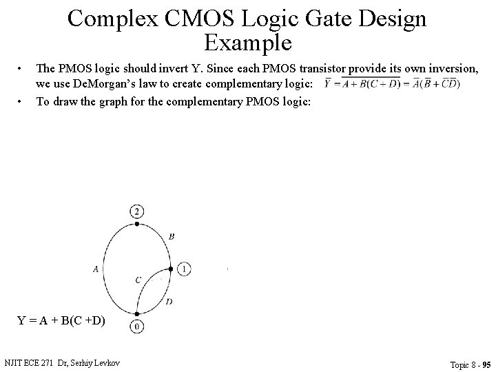
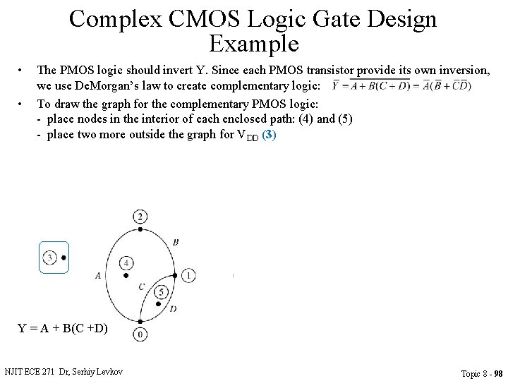
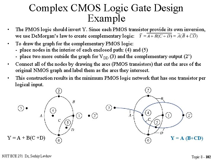
Complex CMOS Logic Gate Design Example • • The PMOS logic should invert Y. Since each PMOS transistor provide its own inversion, we use De. Morgan’s law to create complementary logic: To draw the graph for the complementary PMOS logic: Y = A + B(C +D) NJIT ECE 271 Dr, Serhiy Levkov Topic 8 - 95

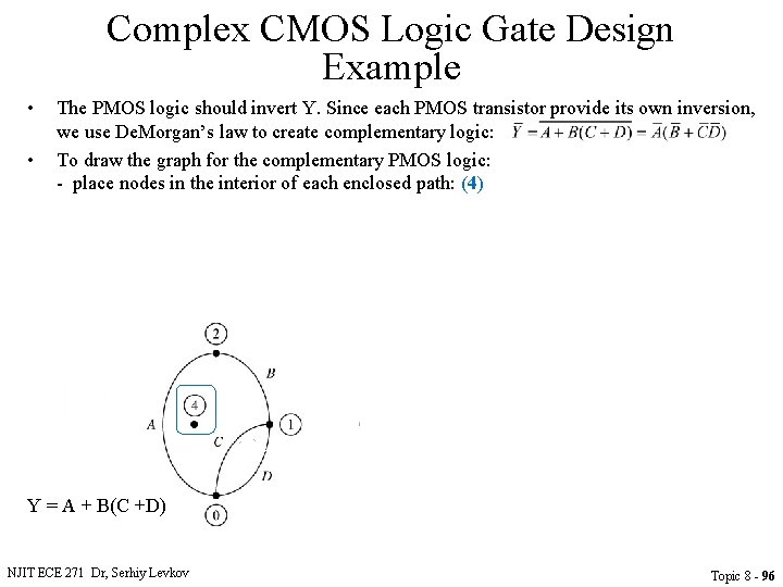
Complex CMOS Logic Gate Design Example • • The PMOS logic should invert Y. Since each PMOS transistor provide its own inversion, we use De. Morgan’s law to create complementary logic: To draw the graph for the complementary PMOS logic: - place nodes in the interior of each enclosed path: (4) Y = A + B(C +D) NJIT ECE 271 Dr, Serhiy Levkov Topic 8 - 96

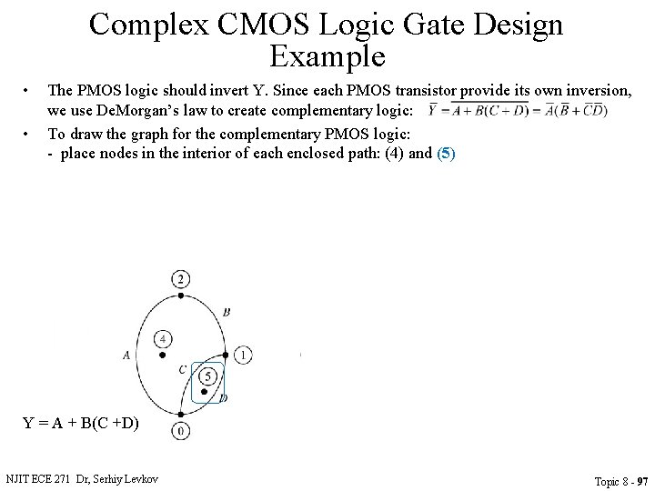
Complex CMOS Logic Gate Design Example • • The PMOS logic should invert Y. Since each PMOS transistor provide its own inversion, we use De. Morgan’s law to create complementary logic: To draw the graph for the complementary PMOS logic: - place nodes in the interior of each enclosed path: (4) and (5) Y = A + B(C +D) NJIT ECE 271 Dr, Serhiy Levkov Topic 8 - 97

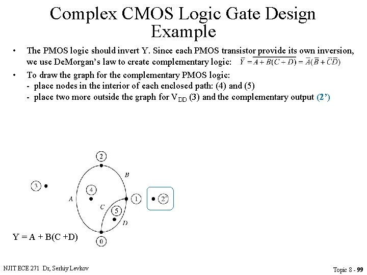
Complex CMOS Logic Gate Design Example • • The PMOS logic should invert Y. Since each PMOS transistor provide its own inversion, we use De. Morgan’s law to create complementary logic: To draw the graph for the complementary PMOS logic: - place nodes in the interior of each enclosed path: (4) and (5) - place two more outside the graph for VDD (3) Y = A + B(C +D) NJIT ECE 271 Dr, Serhiy Levkov Topic 8 - 98

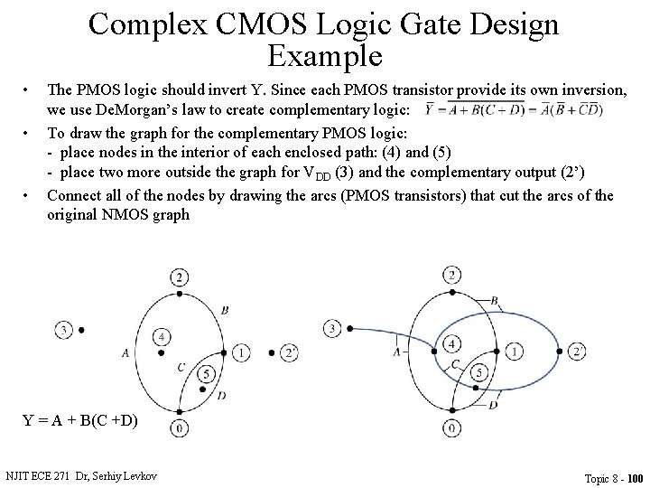
Complex CMOS Logic Gate Design Example • • The PMOS logic should invert Y. Since each PMOS transistor provide its own inversion, we use De. Morgan’s law to create complementary logic: To draw the graph for the complementary PMOS logic: - place nodes in the interior of each enclosed path: (4) and (5) - place two more outside the graph for VDD (3) and the complementary output (2’) Y = A + B(C +D) NJIT ECE 271 Dr, Serhiy Levkov Topic 8 - 99

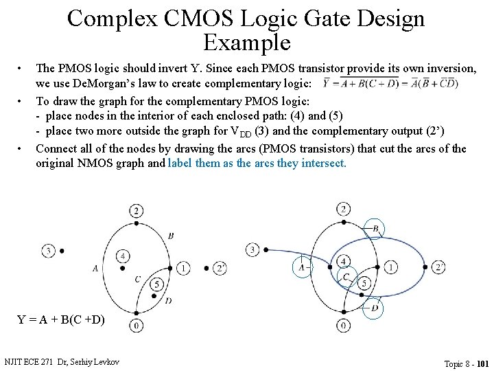
Complex CMOS Logic Gate Design Example • • • The PMOS logic should invert Y. Since each PMOS transistor provide its own inversion, we use De. Morgan’s law to create complementary logic: To draw the graph for the complementary PMOS logic: - place nodes in the interior of each enclosed path: (4) and (5) - place two more outside the graph for VDD (3) and the complementary output (2’) Connect all of the nodes by drawing the arcs (PMOS transistors) that cut the arcs of the original NMOS graph Y = A + B(C +D) NJIT ECE 271 Dr, Serhiy Levkov Topic 8 - 100

Complex CMOS Logic Gate Design Example • • • The PMOS logic should invert Y. Since each PMOS transistor provide its own inversion, we use De. Morgan’s law to create complementary logic: To draw the graph for the complementary PMOS logic: - place nodes in the interior of each enclosed path: (4) and (5) - place two more outside the graph for VDD (3) and the complementary output (2’) Connect all of the nodes by drawing the arcs (PMOS transistors) that cut the arcs of the original NMOS graph and label them as the arcs they intersect. Y = A + B(C +D) NJIT ECE 271 Dr, Serhiy Levkov Topic 8 - 101

Complex CMOS Logic Gate Design Example • • The PMOS logic should invert Y. Since each PMOS transistor provide its own inversion, we use De. Morgan’s law to create complementary logic: To draw the graph for the complementary PMOS logic: - place nodes in the interior of each enclosed path: (4) and (5) - place two more outside the graph for VDD (3) and the complementary output (2’) Connect all of the nodes by drawing the arcs (PMOS transistors) that cut the arcs of the original NMOS graph and label them as the arcs they intersect. This construction results in the minimum PMOS logic network that has one transistor per logical input. Y = A + B(C +D) NJIT ECE 271 Dr, Serhiy Levkov Y = A (B+CD) Topic 8 - 102

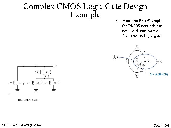
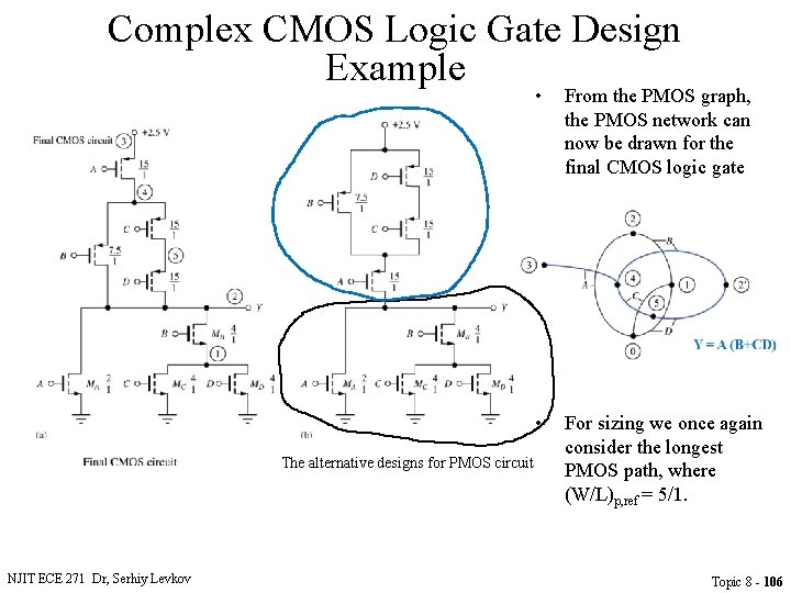
Complex CMOS Logic Gate Design Example • NJIT ECE 271 Dr, Serhiy Levkov From the PMOS graph, the PMOS network can now be drawn for the final CMOS logic gate Topic 8 - 103

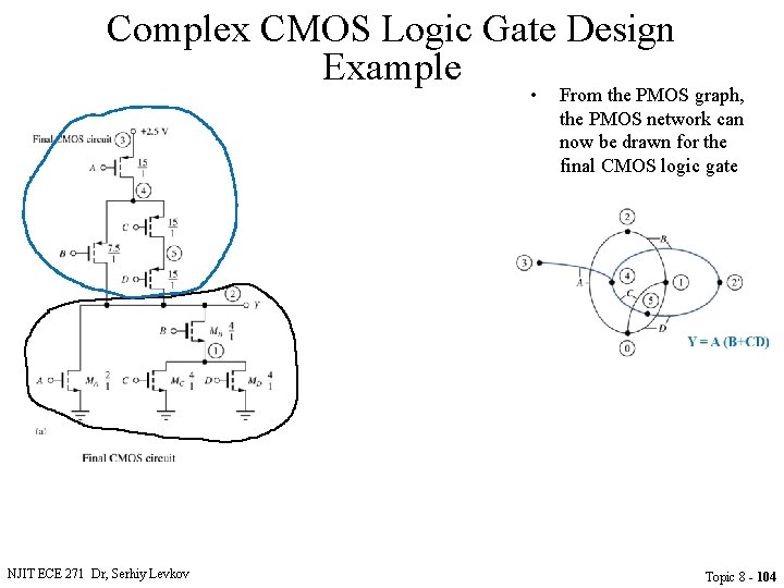
Complex CMOS Logic Gate Design Example • NJIT ECE 271 Dr, Serhiy Levkov From the PMOS graph, the PMOS network can now be drawn for the final CMOS logic gate Topic 8 - 104

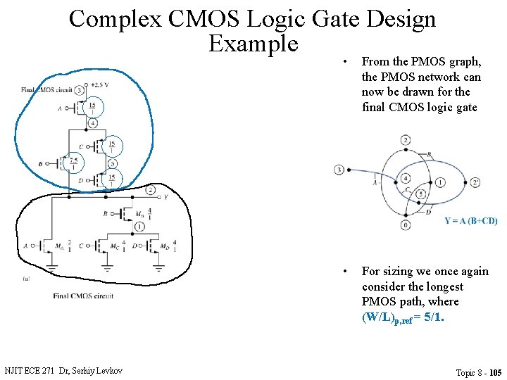
Complex CMOS Logic Gate Design Example NJIT ECE 271 Dr, Serhiy Levkov • From the PMOS graph, the PMOS network can now be drawn for the final CMOS logic gate • For sizing we once again consider the longest PMOS path, where (W/L)p, ref = 5/1. Topic 8 - 105

Complex CMOS Logic Gate Design Example The alternative designs for PMOS circuit NJIT ECE 271 Dr, Serhiy Levkov • From the PMOS graph, the PMOS network can now be drawn for the final CMOS logic gate • For sizing we once again consider the longest PMOS path, where (W/L)p, ref = 5/1. Topic 8 - 106

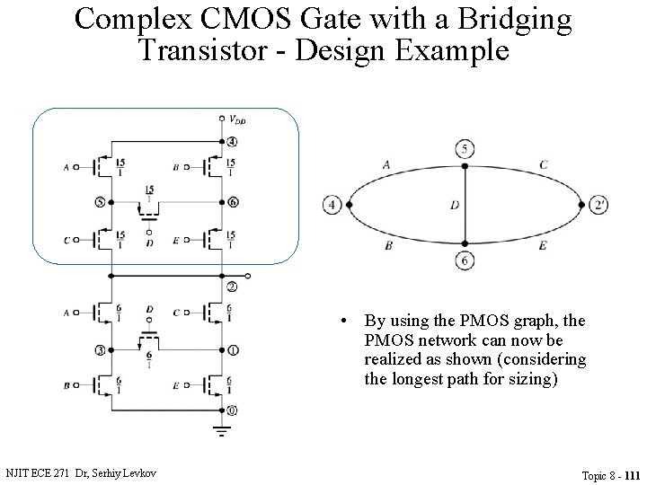
Complex CMOS Gate with a Bridging Transistor - Design Example • Design a CMOS gate that implements the following logic function using the same reference inverter sizes as the previous example: = AB +CE + ADE + CDB NJIT ECE 271 Dr, Serhiy Levkov Y Topic 8 - 107

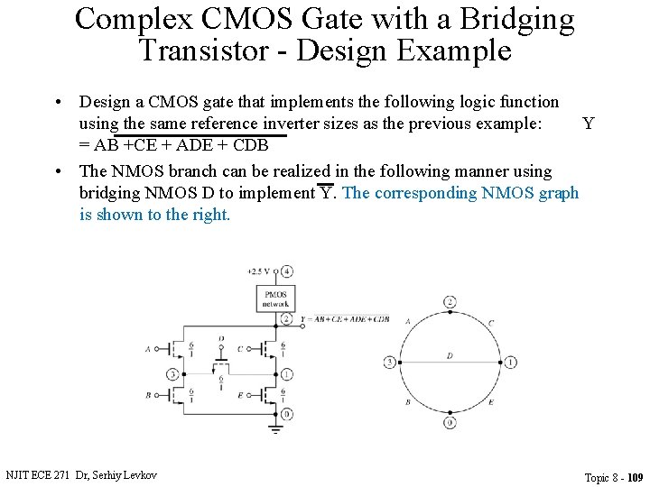
Complex CMOS Gate with a Bridging Transistor - Design Example • Design a CMOS gate that implements the following logic function using the same reference inverter sizes as the previous example: = AB +CE + ADE + CDB • The NMOS branch can be realized in the following manner using bridging NMOS D to implement Y. NJIT ECE 271 Dr, Serhiy Levkov Y Topic 8 - 108

Complex CMOS Gate with a Bridging Transistor - Design Example • Design a CMOS gate that implements the following logic function using the same reference inverter sizes as the previous example: Y = AB +CE + ADE + CDB • The NMOS branch can be realized in the following manner using bridging NMOS D to implement Y. The corresponding NMOS graph is shown to the right. NJIT ECE 271 Dr, Serhiy Levkov Topic 8 - 109

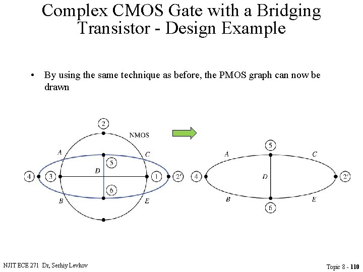
Complex CMOS Gate with a Bridging Transistor - Design Example • By using the same technique as before, the PMOS graph can now be drawn NJIT ECE 271 Dr, Serhiy Levkov Topic 8 - 110

Complex CMOS Gate with a Bridging Transistor - Design Example • By using the PMOS graph, the PMOS network can now be realized as shown (considering the longest path for sizing) NJIT ECE 271 Dr, Serhiy Levkov Topic 8 - 111

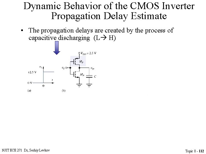
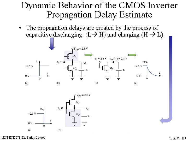
Dynamic Behavior of the CMOS Inverter Propagation Delay Estimate • The propagation delays are created by the process of capacitive discharging (L H) NJIT ECE 271 Dr, Serhiy Levkov Topic 8 - 112

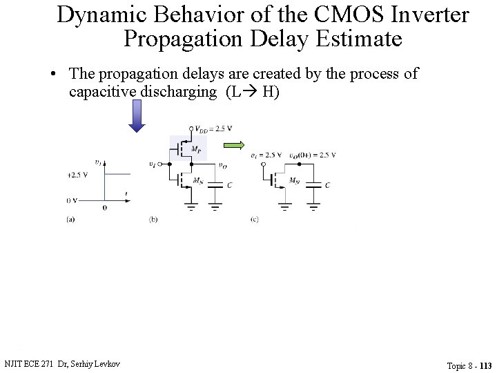
Dynamic Behavior of the CMOS Inverter Propagation Delay Estimate • The propagation delays are created by the process of capacitive discharging (L H) NJIT ECE 271 Dr, Serhiy Levkov Topic 8 - 113

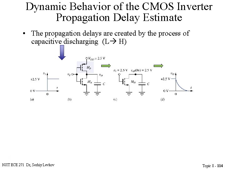
Dynamic Behavior of the CMOS Inverter Propagation Delay Estimate • The propagation delays are created by the process of capacitive discharging (L H) NJIT ECE 271 Dr, Serhiy Levkov Topic 8 - 114

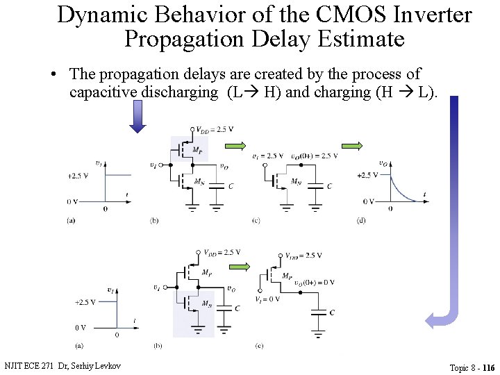
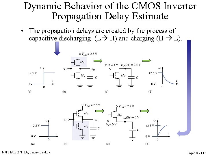
Dynamic Behavior of the CMOS Inverter Propagation Delay Estimate • The propagation delays are created by the process of capacitive discharging (L H) and charging (H L). NJIT ECE 271 Dr, Serhiy Levkov Topic 8 - 115

Dynamic Behavior of the CMOS Inverter Propagation Delay Estimate • The propagation delays are created by the process of capacitive discharging (L H) and charging (H L). NJIT ECE 271 Dr, Serhiy Levkov Topic 8 - 116

Dynamic Behavior of the CMOS Inverter Propagation Delay Estimate • The propagation delays are created by the process of capacitive discharging (L H) and charging (H L). NJIT ECE 271 Dr, Serhiy Levkov Topic 8 - 117

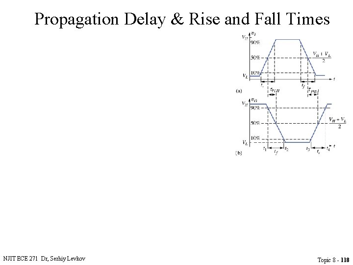
Propagation Delay & Rise and Fall Times NJIT ECE 271 Dr, Serhiy Levkov Topic 8 - 118

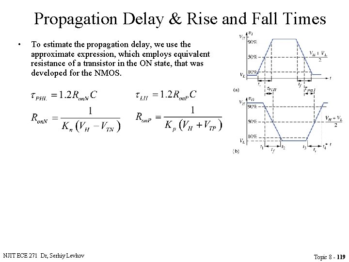
Propagation Delay & Rise and Fall Times • To estimate the propagation delay, we use the approximate expression, which employs equivalent resistance of a transistor in the ON state, that was developed for the NMOS. NJIT ECE 271 Dr, Serhiy Levkov Topic 8 - 119

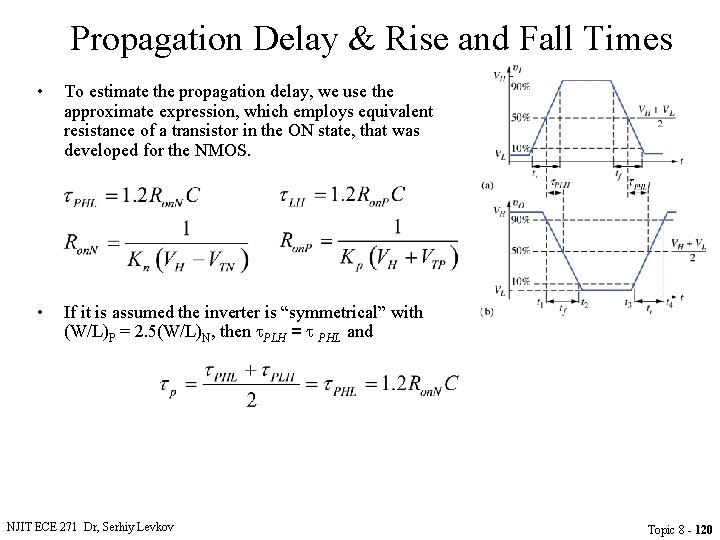
Propagation Delay & Rise and Fall Times • To estimate the propagation delay, we use the approximate expression, which employs equivalent resistance of a transistor in the ON state, that was developed for the NMOS. • If it is assumed the inverter is “symmetrical” with (W/L)P = 2. 5(W/L)N, then PLH = PHL and NJIT ECE 271 Dr, Serhiy Levkov Topic 8 - 120

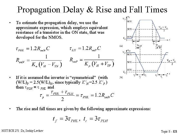
Propagation Delay & Rise and Fall Times • To estimate the propagation delay, we use the approximate expression, which employs equivalent resistance of a transistor in the ON state, that was developed for the NMOS. • If it is assumed the inverter is “symmetrical” (with (W/L)P = 2. 5(W/L)N, since typically K’N =2. 5 K’P ) then PLH = PHL and • The rise and fall times are given by the following approximate expressions: NJIT ECE 271 Dr, Serhiy Levkov Topic 8 - 121

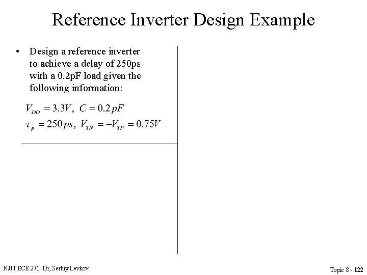
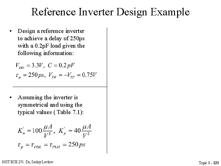
Reference Inverter Design Example • Design a reference inverter to achieve a delay of 250 ps with a 0. 2 p. F load given the following information: NJIT ECE 271 Dr, Serhiy Levkov Topic 8 - 122

Reference Inverter Design Example • Design a reference inverter to achieve a delay of 250 ps with a 0. 2 p. F load given the following information: • Assuming the inverter is symmetrical and using the typical values ( Table 7. 1): NJIT ECE 271 Dr, Serhiy Levkov Topic 8 - 123

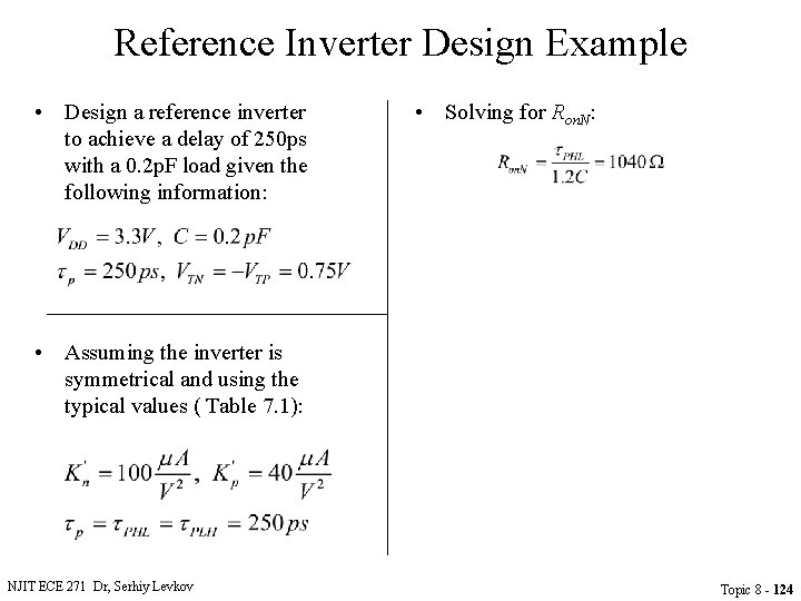
Reference Inverter Design Example • Design a reference inverter to achieve a delay of 250 ps with a 0. 2 p. F load given the following information: • Solving for Ron. N: • Assuming the inverter is symmetrical and using the typical values ( Table 7. 1): NJIT ECE 271 Dr, Serhiy Levkov Topic 8 - 124

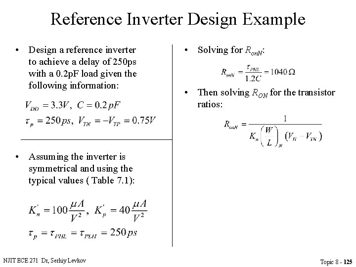
Reference Inverter Design Example • Design a reference inverter to achieve a delay of 250 ps with a 0. 2 p. F load given the following information: • Solving for Ron. N: • Then solving RON for the transistor ratios: • Assuming the inverter is symmetrical and using the typical values ( Table 7. 1): NJIT ECE 271 Dr, Serhiy Levkov Topic 8 - 125

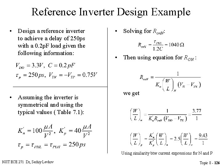
Reference Inverter Design Example • Design a reference inverter to achieve a delay of 250 ps with a 0. 2 p. F load given the following information: • Assuming the inverter is symmetrical and using the typical values ( Table 7. 1): • Solving for Ron. N: • Then using equation for RON : we get Using similarity btw current expressions for N and P NJIT ECE 271 Dr, Serhiy Levkov Topic 8 - 126

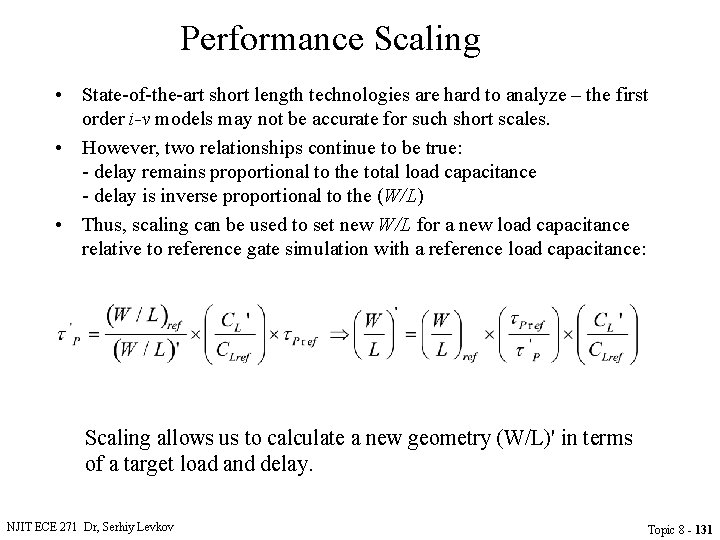
Performance Scaling • State-of-the-art short length technologies are hard to analyze – the first order i-v models may not be accurate for such short scales. NJIT ECE 271 Dr, Serhiy Levkov Topic 8 - 127

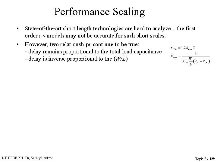
Performance Scaling • State-of-the-art short length technologies are hard to analyze – the first order i-v models may not be accurate for such short scales. • However, two relationships continue to be true: - delay remains proportional to the total load capacitance NJIT ECE 271 Dr, Serhiy Levkov Topic 8 - 128

Performance Scaling • State-of-the-art short length technologies are hard to analyze – the first order i-v models may not be accurate for such short scales. • However, two relationships continue to be true: - delay remains proportional to the total load capacitance - delay is inverse proportional to the (W/L) NJIT ECE 271 Dr, Serhiy Levkov Topic 8 - 129

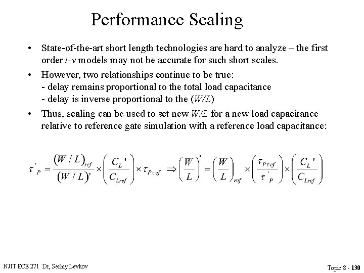
Performance Scaling • State-of-the-art short length technologies are hard to analyze – the first order i-v models may not be accurate for such short scales. • However, two relationships continue to be true: - delay remains proportional to the total load capacitance - delay is inverse proportional to the (W/L) • Thus, scaling can be used to set new W/L for a new load capacitance relative to reference gate simulation with a reference load capacitance: NJIT ECE 271 Dr, Serhiy Levkov Topic 8 - 130

Performance Scaling • State-of-the-art short length technologies are hard to analyze – the first order i-v models may not be accurate for such short scales. • However, two relationships continue to be true: - delay remains proportional to the total load capacitance - delay is inverse proportional to the (W/L) • Thus, scaling can be used to set new W/L for a new load capacitance relative to reference gate simulation with a reference load capacitance: Scaling allows us to calculate a new geometry (W/L)' in terms of a target load and delay. NJIT ECE 271 Dr, Serhiy Levkov Topic 8 - 131

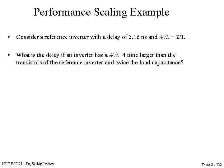
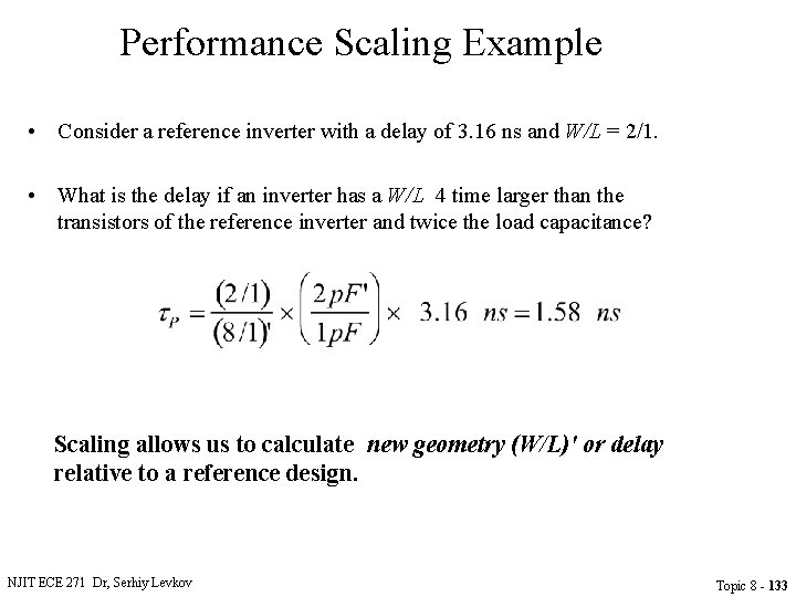
Performance Scaling Example • Consider a reference inverter with a delay of 3. 16 ns and W/L = 2/1. • What is the delay if an inverter has a W/L 4 time larger than the transistors of the reference inverter and twice the load capacitance? NJIT ECE 271 Dr, Serhiy Levkov Topic 8 - 132

Performance Scaling Example • Consider a reference inverter with a delay of 3. 16 ns and W/L = 2/1. • What is the delay if an inverter has a W/L 4 time larger than the transistors of the reference inverter and twice the load capacitance? Scaling allows us to calculate new geometry (W/L)' or delay relative to a reference design. NJIT ECE 271 Dr, Serhiy Levkov Topic 8 - 133

Static Power Dissipation • CMOS logic is considered to have no static power dissipation. NJIT ECE 271 Dr, Serhiy Levkov Topic 8 - 134

Static Power Dissipation • • CMOS logic is considered to have no static power dissipation. This is not completely accurate since MOS transistors have leakage currents associated with the reverse-biased drain-to-substrate connections as well as sub-threshold leakage current between the drain and source. NJIT ECE 271 Dr, Serhiy Levkov Topic 8 - 135

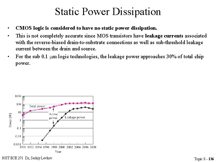
Static Power Dissipation • • • CMOS logic is considered to have no static power dissipation. This is not completely accurate since MOS transistors have leakage currents associated with the reverse-biased drain-to-substrate connections as well as sub-threshold leakage current between the drain and source. For the sub 0. 1 mm logic technologies, the leakage power approaches 30% of total chip power. NJIT ECE 271 Dr, Serhiy Levkov Topic 8 - 136

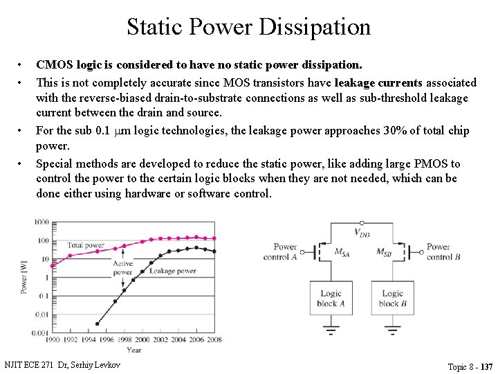
Static Power Dissipation • • CMOS logic is considered to have no static power dissipation. This is not completely accurate since MOS transistors have leakage currents associated with the reverse-biased drain-to-substrate connections as well as sub-threshold leakage current between the drain and source. For the sub 0. 1 mm logic technologies, the leakage power approaches 30% of total chip power. Special methods are developed to reduce the static power, like adding large PMOS to control the power to the certain logic blocks when they are not needed, which can be done either using hardware or software control. NJIT ECE 271 Dr, Serhiy Levkov Topic 8 - 137

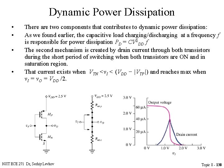
Dynamic Power Dissipation • • There are two components that contributes to dynamic power dissipation: As we found earlier, the capacitive load charging/discharging at a frequency f is responsible for power dissipation PD = CV 2 DD f The second mechanism is created by drain current through both transistors during the short period of switching when both transistors are ON and in saturation region. That current exists when VTN <v. I < (VDD − |VTP|) and reaches max when v. I = v. O = VDD /2. NJIT ECE 271 Dr, Serhiy Levkov Topic 8 - 138

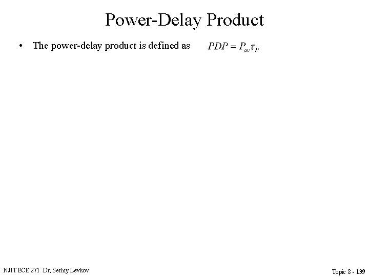
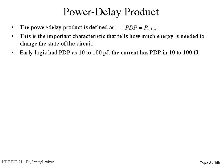
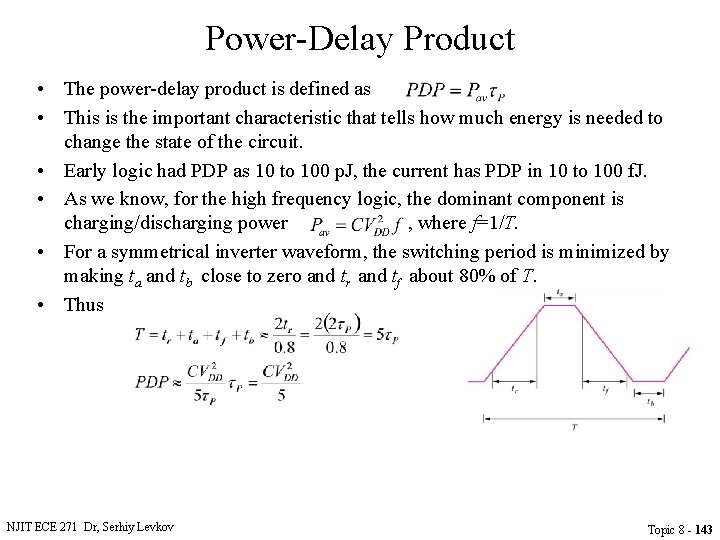
Power-Delay Product • The power-delay product is defined as NJIT ECE 271 Dr, Serhiy Levkov Topic 8 - 139

Power-Delay Product • The power-delay product is defined as • This is the important characteristic that tells how much energy is needed to change the state of the circuit. • Early logic had PDP as 10 to 100 p. J, the current has PDP in 10 to 100 f. J. NJIT ECE 271 Dr, Serhiy Levkov Topic 8 - 140

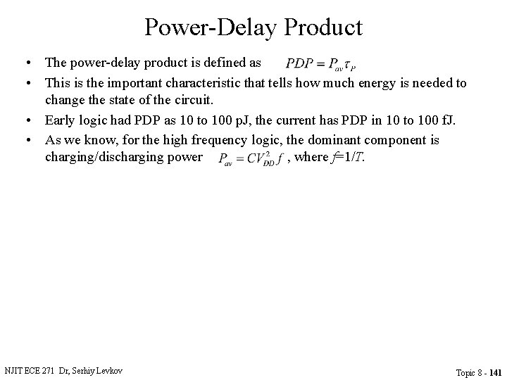
Power-Delay Product • The power-delay product is defined as • This is the important characteristic that tells how much energy is needed to change the state of the circuit. • Early logic had PDP as 10 to 100 p. J, the current has PDP in 10 to 100 f. J. • As we know, for the high frequency logic, the dominant component is charging/discharging power , where f=1/T. NJIT ECE 271 Dr, Serhiy Levkov Topic 8 - 141

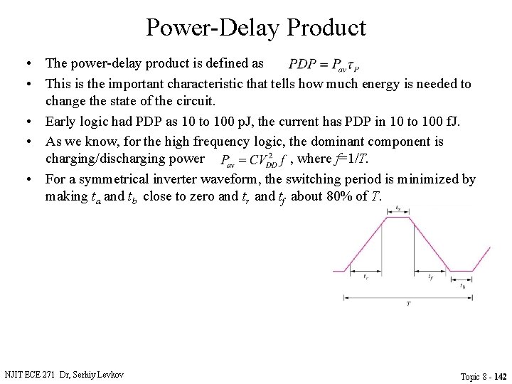
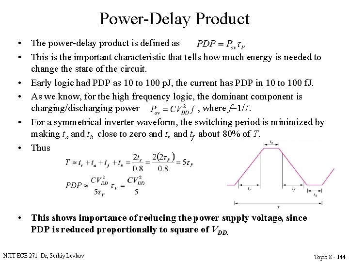
Power-Delay Product • The power-delay product is defined as • This is the important characteristic that tells how much energy is needed to change the state of the circuit. • Early logic had PDP as 10 to 100 p. J, the current has PDP in 10 to 100 f. J. • As we know, for the high frequency logic, the dominant component is charging/discharging power , where f=1/T. • For a symmetrical inverter waveform, the switching period is minimized by making ta and tb close to zero and tr and tf about 80% of T. NJIT ECE 271 Dr, Serhiy Levkov Topic 8 - 142

Power-Delay Product • The power-delay product is defined as • This is the important characteristic that tells how much energy is needed to change the state of the circuit. • Early logic had PDP as 10 to 100 p. J, the current has PDP in 10 to 100 f. J. • As we know, for the high frequency logic, the dominant component is charging/discharging power , where f=1/T. • For a symmetrical inverter waveform, the switching period is minimized by making ta and tb close to zero and tr and tf about 80% of T. • Thus NJIT ECE 271 Dr, Serhiy Levkov Topic 8 - 143

Power-Delay Product • The power-delay product is defined as • This is the important characteristic that tells how much energy is needed to change the state of the circuit. • Early logic had PDP as 10 to 100 p. J, the current has PDP in 10 to 100 f. J. • As we know, for the high frequency logic, the dominant component is charging/discharging power , where f=1/T. • For a symmetrical inverter waveform, the switching period is minimized by making ta and tb close to zero and tr and tf about 80% of T. • Thus • This shows importance of reducing the power supply voltage, since PDP is reduced proportionally to square of VDD. NJIT ECE 271 Dr, Serhiy Levkov Topic 8 - 144

Minimum Size Gate Design and Performance • With CMOS technology, there is an design area/propagation delay tradeoff that needs to be considered. NJIT ECE 271 Dr, Serhiy Levkov Topic 8 - 145

Minimum Size Gate Design and Performance • With CMOS technology, there is an design area/propagation delay tradeoff that needs to be considered. • In the AND sequences, in order to minimize delay we want to provide the max current and has to increase the width of design. NJIT ECE 271 Dr, Serhiy Levkov Topic 8 - 146

Minimum Size Gate Design and Performance • With CMOS technology, there is an design area/propagation delay tradeoff that needs to be considered. • In the AND sequences, in order to minimize delay we want to provide the max current and has to increase the width of design. • However this increases the total design area and the density of transistors. NJIT ECE 271 Dr, Serhiy Levkov Topic 8 - 147

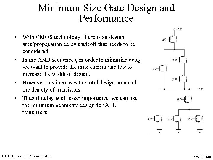
Minimum Size Gate Design and Performance • With CMOS technology, there is an design area/propagation delay tradeoff that needs to be considered. • In the AND sequences, in order to minimize delay we want to provide the max current and has to increase the width of design. • However this increases the total design area and the density of transistors. • Thus if delay is of lesser importance, we can use the minimum geometry design for ALL transistors NJIT ECE 271 Dr, Serhiy Levkov Topic 8 - 148

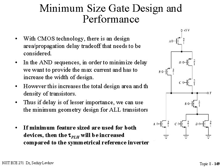
Minimum Size Gate Design and Performance • With CMOS technology, there is an design area/propagation delay tradeoff that needs to be considered. • In the AND sequences, in order to minimize delay we want to provide the max current and has to increase the width of design. • However this increases the total design area and the density of transistors. • Thus if delay is of lesser importance, we can use the minimum geometry design for ALL transistors • If minimum feature sized are used for both devices, then the PLH will be increased compared to the symmetrical reference inverter NJIT ECE 271 Dr, Serhiy Levkov Topic 8 - 149