Chapter 10 Digital CMOS Logic Circuits 10 1


 Small size, ease of fabrication")
 had been used for many years. • ECL (Emitter")

 of")


 of")


")
")


- Slides: 84
Chapter 10 Digital CMOS Logic Circuits • 10. 1 Digital circuit design : An overview • 10. 2 Design and performance analysis of the CMOS inverter • 10. 3 CMOS logic gate circuits • 10. 4 Pseudo- NMOS logic circuits
10. 1 Digital circuit Design : An Overview 10. 1. 1 Digital IC technologies and logic circuit families Fig. 10. 1 Digital IC technologies and logic circuit families
CMOS • • Replaced NMOS (much lower power dissipation) Small size, ease of fabrication Channel length has decreased significantly (as short as 0. 06 µm or shorter) Low power dissipation than bipolar logic circuits ( can pack more). High input impedance of MOS transistors can be used to storage charge temporarily (not in bipolar) High levels of integration for both logic (chapter 10) and memory circuits (chapter 11). Dynamic logic to further reduce power dissipation and to increase speed performance.
Bipolar • TTL (Transistor-transistor logic) had been used for many years. • ECL (Emitter –Coupled Logic) : basic element is the differential BJT pair in chapter 7. • Bi. CMOS : combines the high speed of BJT’s with low power dissipation of CMOS. • Ga. As : for very high speed due to the high carrier mobility. Has not demonstrated its potential commercially.
Features to be Considered • • Interface circuits for different families Logic flexibility Speed Complex functions Noise immunity Temperature Power dissipation Co$t
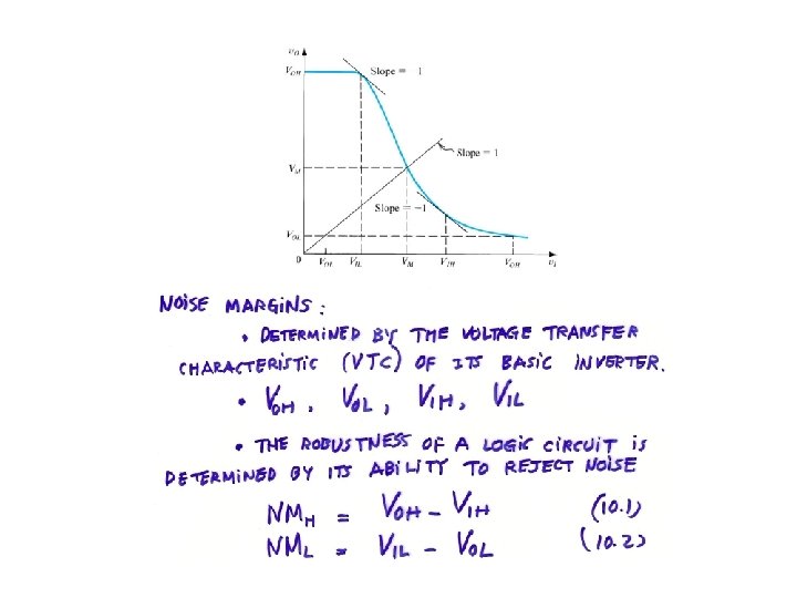
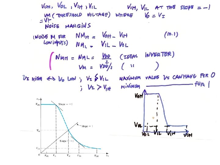
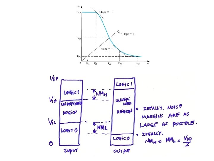
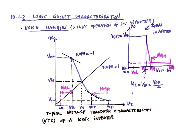
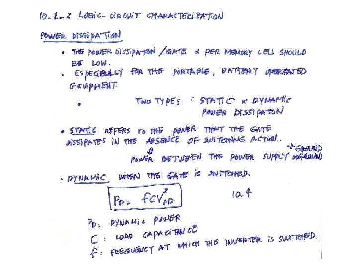
10. 1. 2 Logic circuit characterization Fig. 10. 2 Typical voltage transfer (VTC) of a logic inverter.
Fig. 10. 3 Definitions of propagation delays and switching times of the logic inverter
Fan-In and Fan -Out • Fan-in of a gate : number of inputs. • Fan-out : maximum number of similar gates that a gate can drive while remaining within guaranteed specifications (to keep NMH above certain minimum).
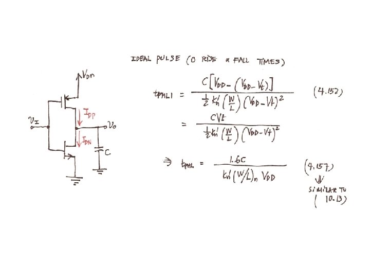
10. 2 Design and performance analysis of the CMOS inverter. 10. 2. 1 Circuit structure Fig. 10. 4 (a) The CMOS inverter and (b) its representation as a pair of switches operated in a complementary fashion.
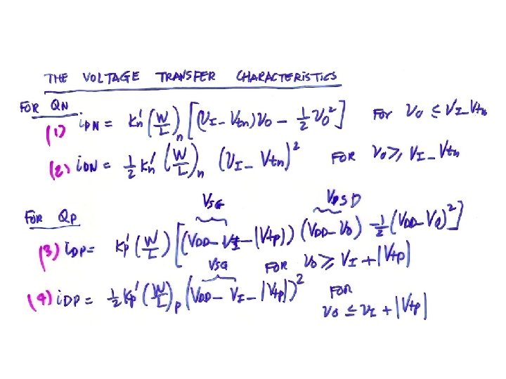
10. 2. 2 Static operation
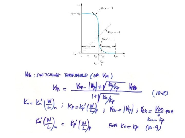
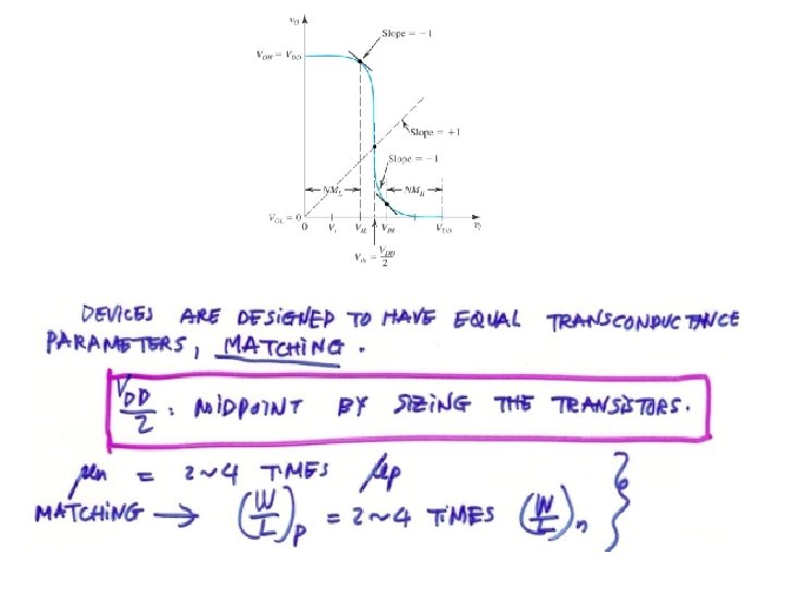
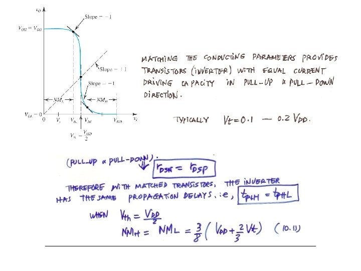
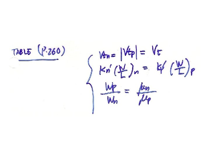
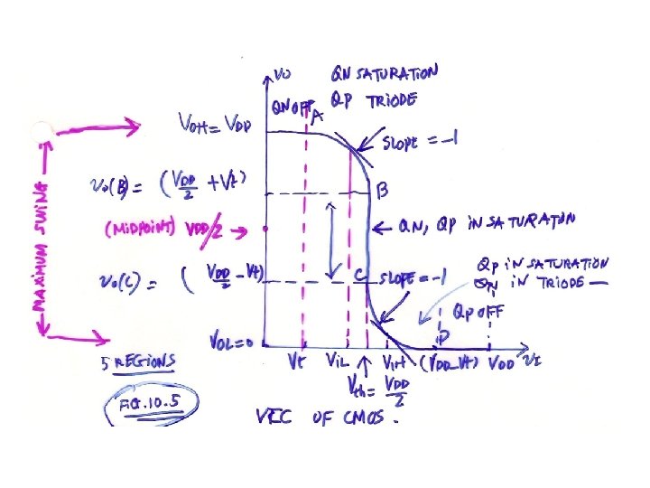
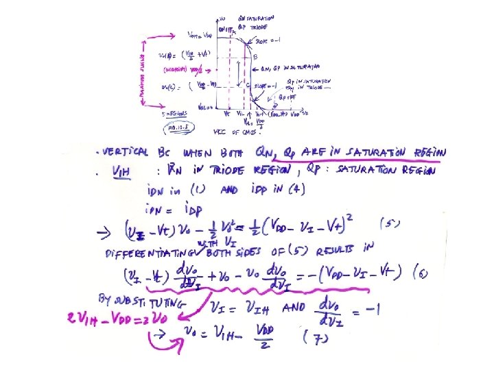
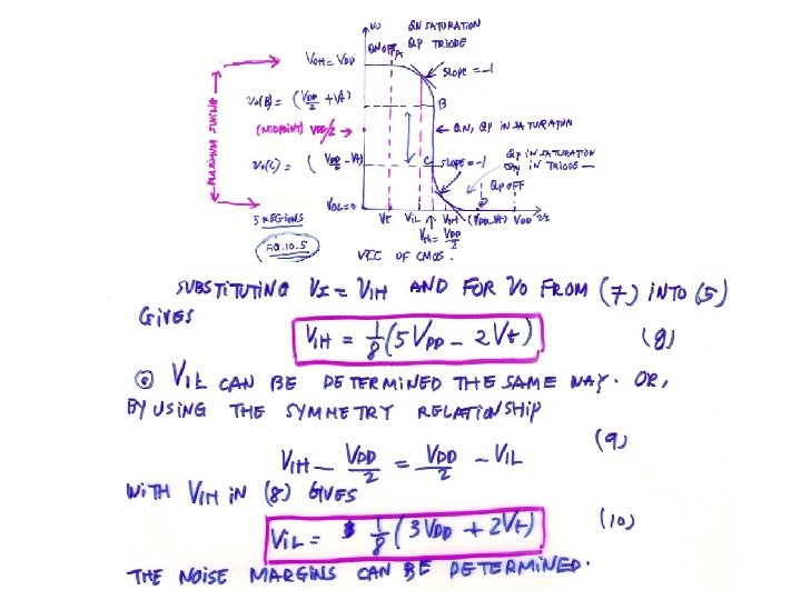
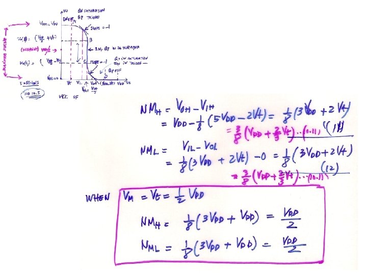
10. 2. 2 Static operation Fig. 10. 5 The voltage transfer characteristic (VTC) of the CMOS inverter when QN and QP are matched
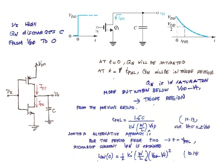
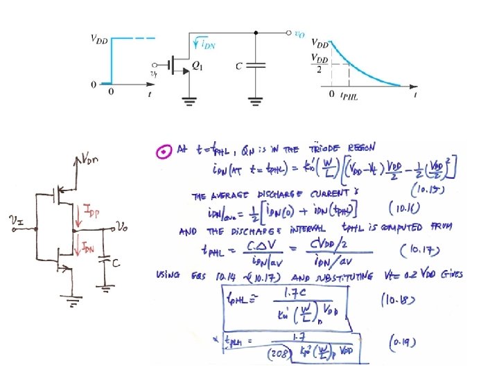
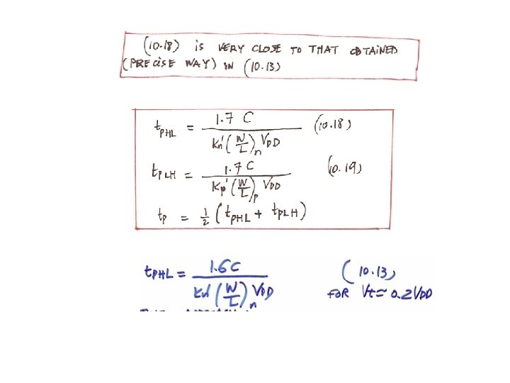
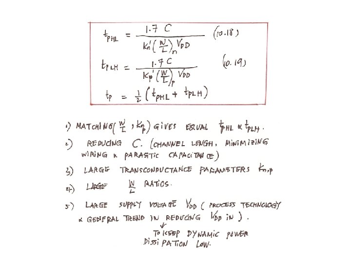
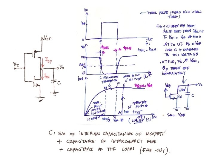
10. 2. 3 Dynamic Operation Fig. 10. 6 Circuit for analyzing the propagation delay of the inverter
Fig. 10. 7 Equivalent circuits for determining the propagation delays
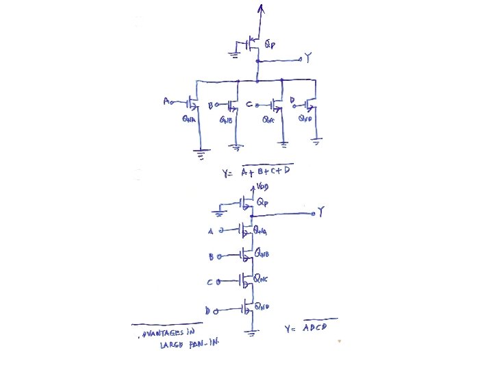
10. 3 CMOS Logic Gate Circuits 10. 3. 1 Basic structure Fig. 10. 8 Representation of a three- input CMOS logic gate
Fig. 10 Examples of pull –down networks (PDN)
Fig. 10 Examples of pull- up networks (PUN)
Fig. 10. 11 Usual and alternative symbols for MOSFETs
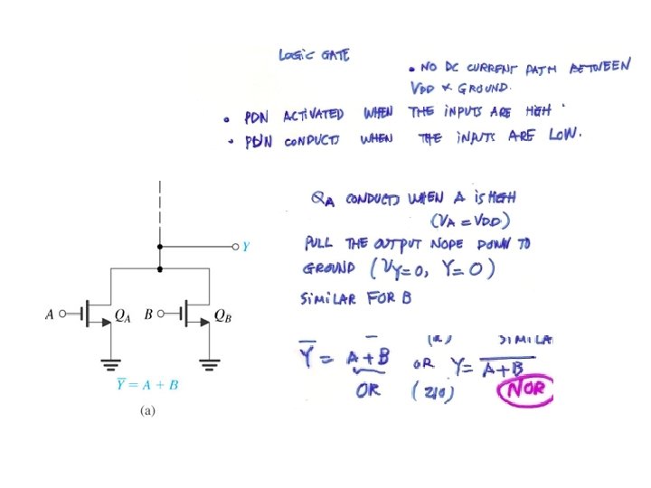
10. 3. 2 The Two – Input NOR Gate Fig. 10. 12 A two – input CMOS NOR gate
10. 3. 3 The Two- Input NAND Gate Fig. 10. 13 A two-input CMOS NAND gate
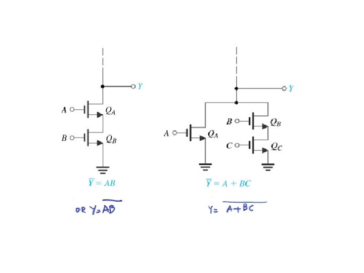
10. 3. 4 A Complex Gate
10. 3. 5 Obtaining the PUN and the PDN and Vice Versa Fig. 10. 14 CMOS realization of a complex gate
10. 3. 6 The Exclusive- OR Function Fig. 10. 15 Realization of the exclusive –OR (XOR) function.
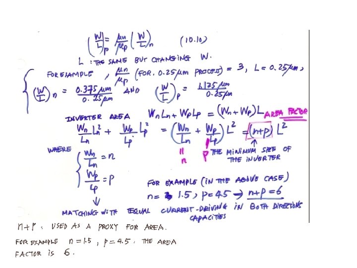
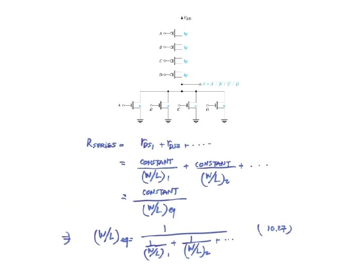
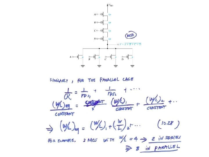
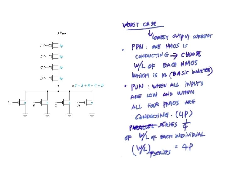
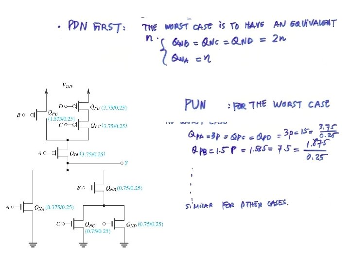
10. 3. 8 Transistor Sizing Fig. 10. 16 Proper transistor sizing for a four- input NOR gate
Fig. 10. 17 Proper transistor sizing for a four- input NAND gate
Fig. 10. 18 Circuit for Example 10. 2
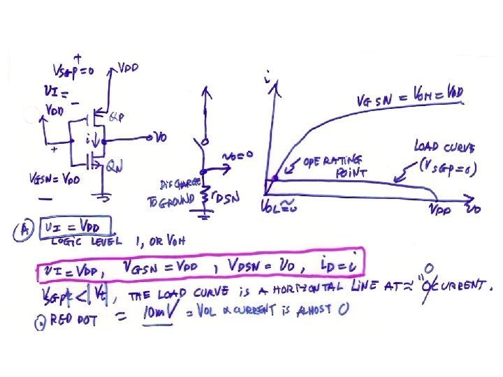
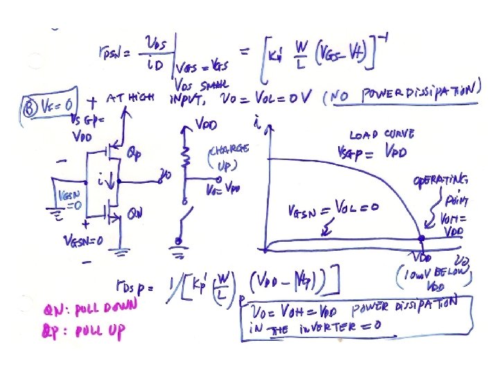
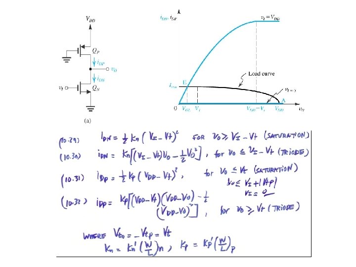
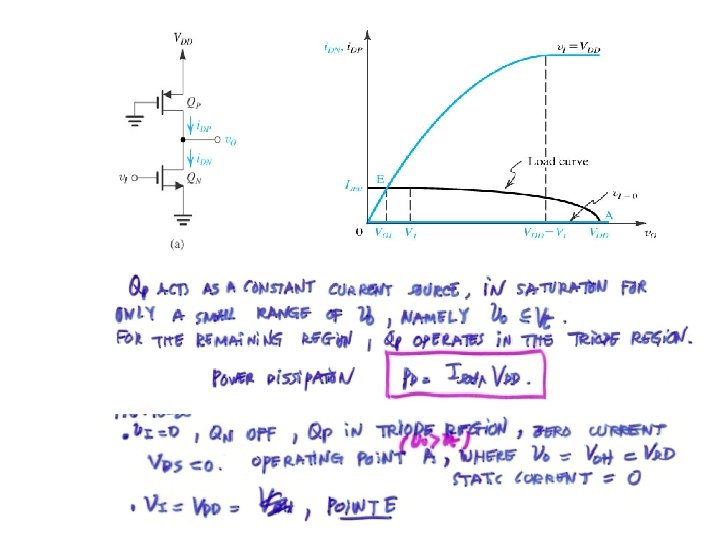
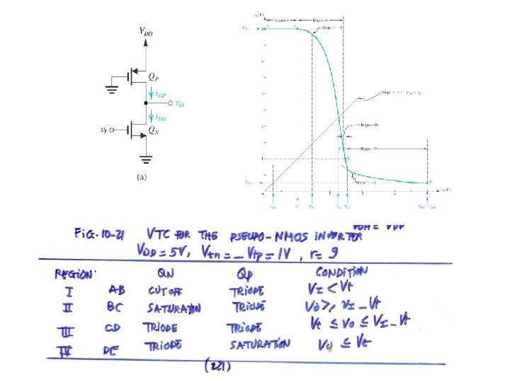
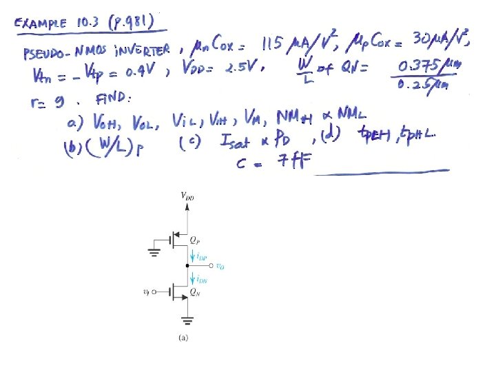
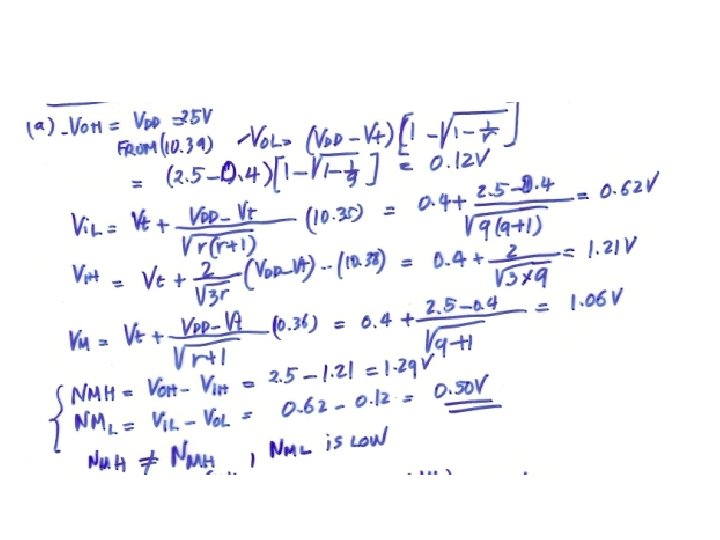
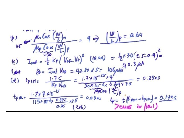
10. 4 Pseudo- NMOS Logic Circuits 10. 4. 1 The pseudo – NMOS inverter Fig. 10. 19 (a) The pseudo- NMOS logic inverter. (b) The enhancement load NMOS inverter (c) The depletion- load NMOS inverter
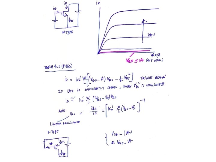
Fig. 4 -2. The enhancement-type NMOS transistor with applied voltage
The I-V characteristic of MOSFET
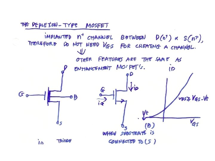
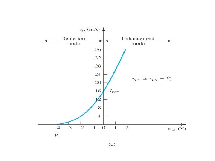
The n- channel depletion –type MOSFET
The depletion type n-channel MOSFET
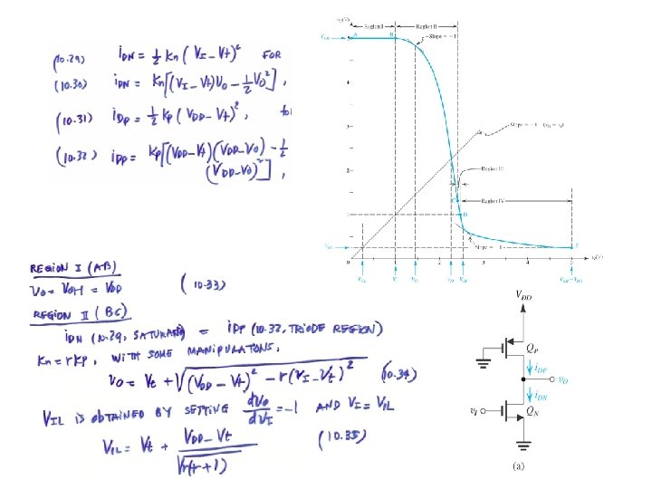
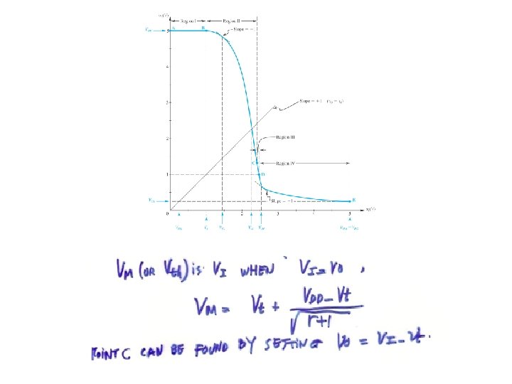
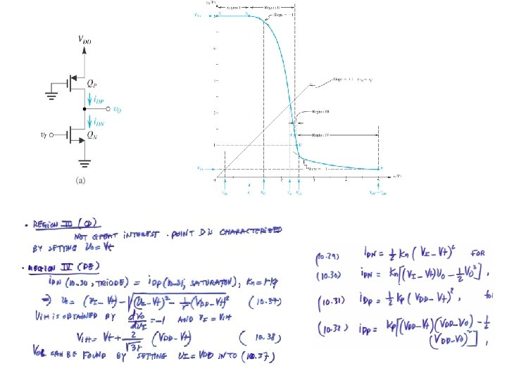
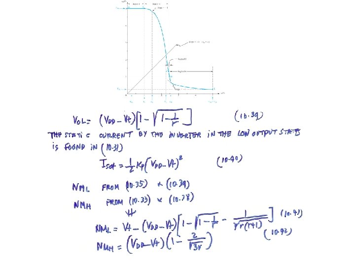
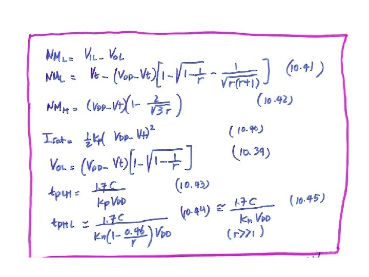
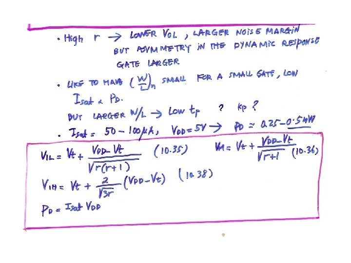
10. 4. 2 Static Characteristics Fig. 10. 20 Graphical construction to determine the VTC of the inverter
Fig. 10. 21 VTC for the pseudo- NMOS inverter.
10. 4. 4 Dynamic Operation