Digital Design Optimizations and Tradeoffs Chapter 6 Optimizations


- Slides: 70

Digital Design – Optimizations and Tradeoffs Chapter 6 Optimizations and Tradeoffs

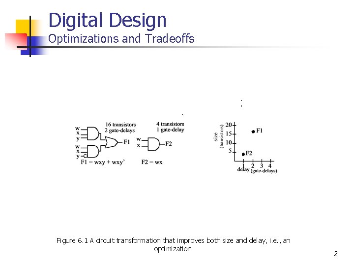
Digital Design Optimizations and Tradeoffs Figure 6. 1 A circuit transformation that improves both size and delay, i. e. , an optimization. 2

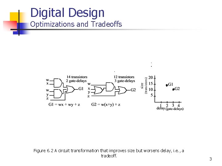
Digital Design Optimizations and Tradeoffs Figure 6. 2 A circuit transformation that improves size but worsens delay, i. e. , a tradeoff. 3

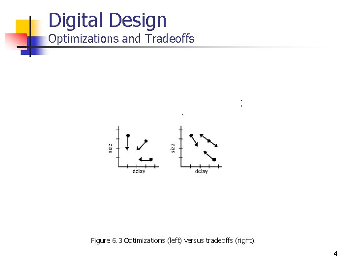
Digital Design Optimizations and Tradeoffs Figure 6. 3 Optimizations (left) versus tradeoffs (right). 4

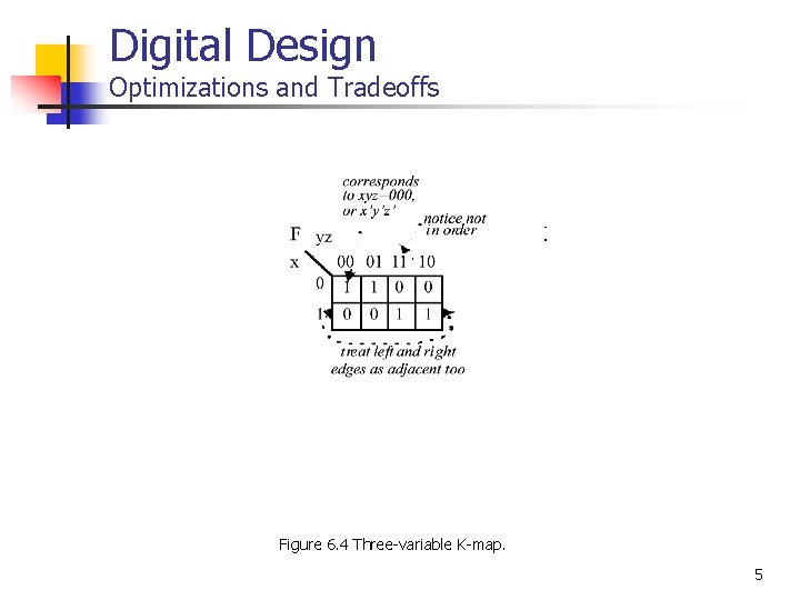
Digital Design Optimizations and Tradeoffs Figure 6. 4 Three-variable K-map. 5

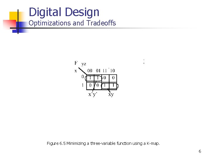
Digital Design Optimizations and Tradeoffs Figure 6. 5 Minimizing a three-variable function using a K-map. 6

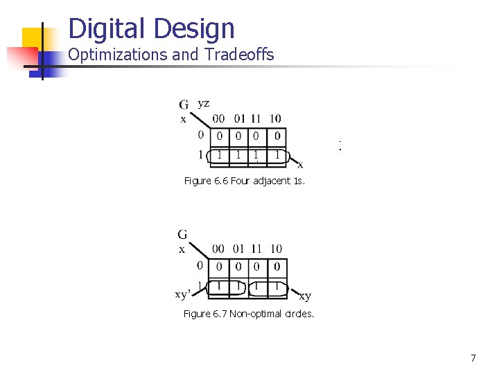
Digital Design Optimizations and Tradeoffs Figure 6. 6 Four adjacent 1 s. Figure 6. 7 Non-optimal circles. 7

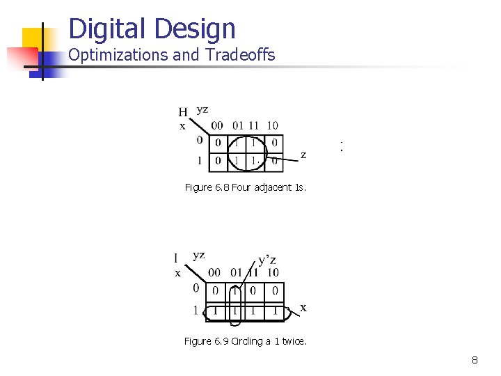
Digital Design Optimizations and Tradeoffs Figure 6. 8 Four adjacent 1 s. Figure 6. 9 Circling a 1 twice. 8

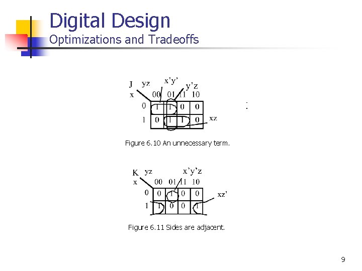
Digital Design Optimizations and Tradeoffs Figure 6. 10 An unnecessary term. Figure 6. 11 Sides are adjacent. 9

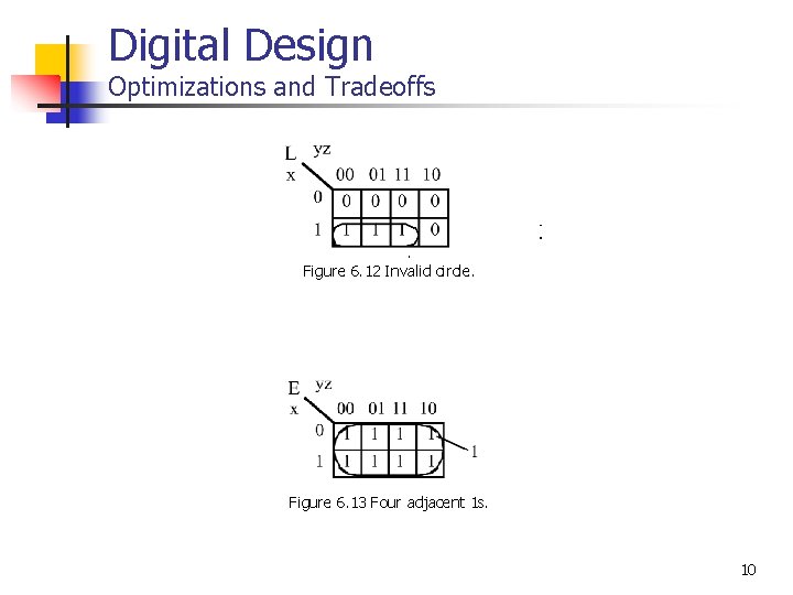
Digital Design Optimizations and Tradeoffs Figure 6. 12 Invalid circle. Figure 6. 13 Four adjacent 1 s. 10

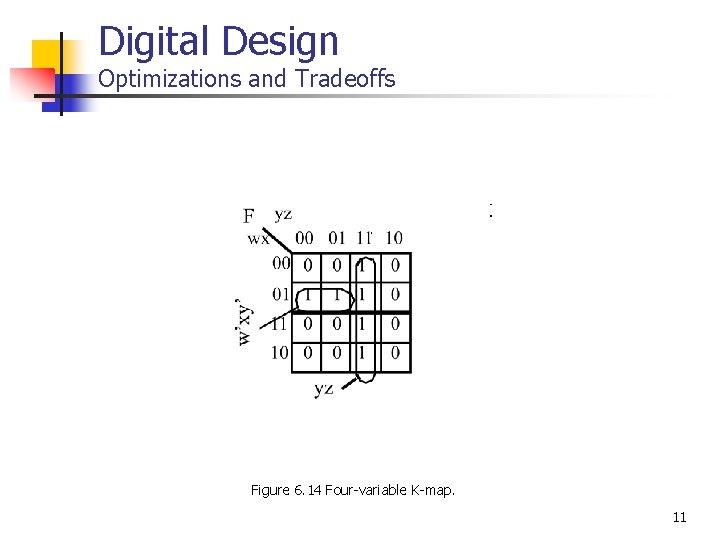
Digital Design Optimizations and Tradeoffs Figure 6. 14 Four-variable K-map. 11

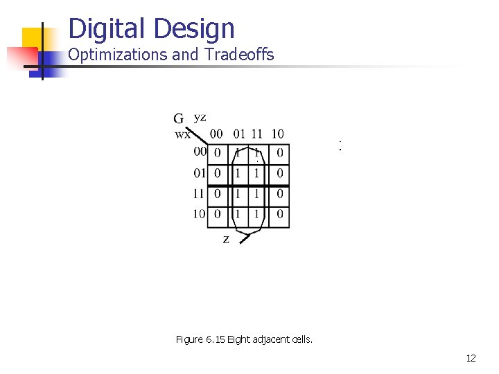
Digital Design Optimizations and Tradeoffs Figure 6. 15 Eight adjacent cells. 12

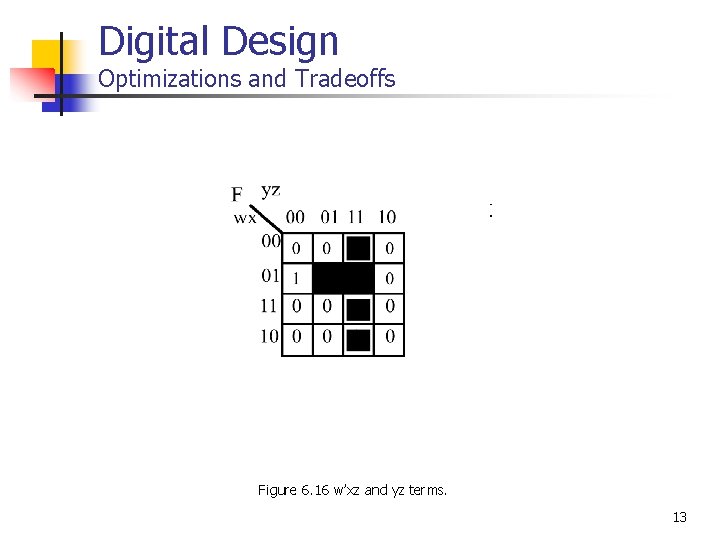
Digital Design Optimizations and Tradeoffs Figure 6. 16 w’xz and yz terms. 13

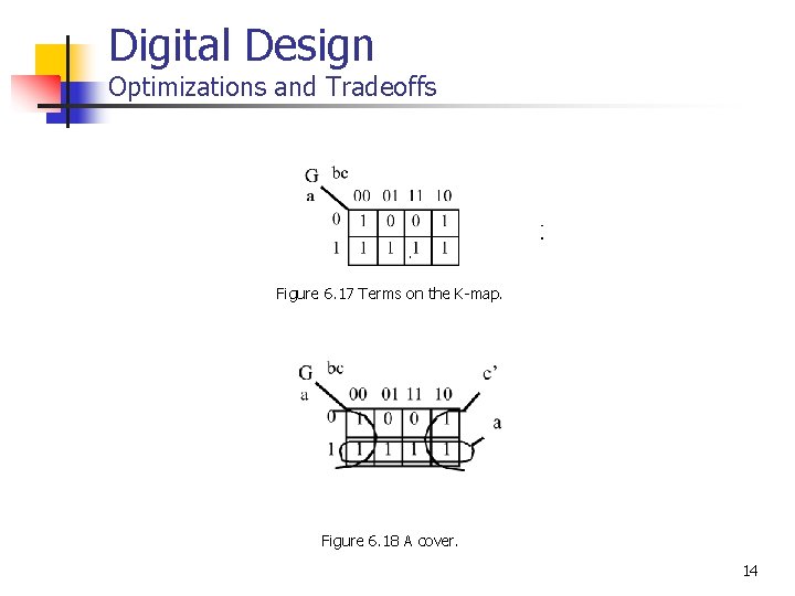
Digital Design Optimizations and Tradeoffs Figure 6. 17 Terms on the K-map. Figure 6. 18 A cover. 14

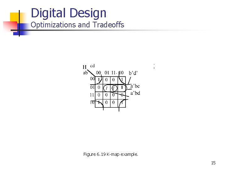
Digital Design Optimizations and Tradeoffs Figure 6. 19 K-map example. 15

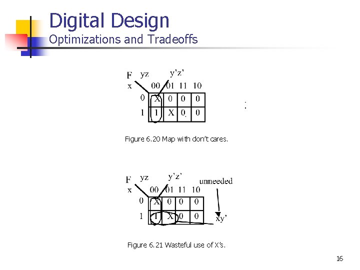
Digital Design Optimizations and Tradeoffs Figure 6. 20 Map with don’t cares. Figure 6. 21 Wasteful use of X’s. 16

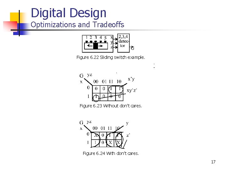
Digital Design Optimizations and Tradeoffs Figure 6. 22 Sliding switch example. Figure 6. 23 Without don’t cares. Figure 6. 24 With don’t cares. 17

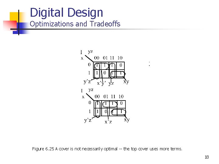
Digital Design Optimizations and Tradeoffs Figure 6. 25 A cover is not necessarily optimal -- the top cover uses more terms. 18

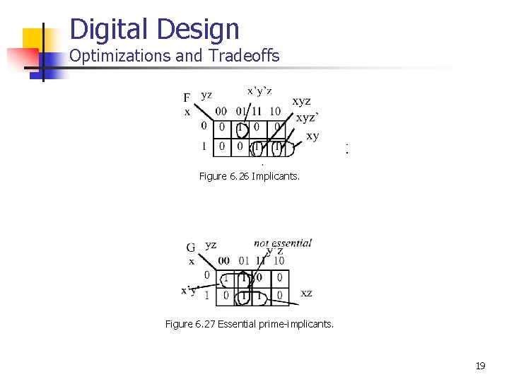
Digital Design Optimizations and Tradeoffs Figure 6. 26 Implicants. Figure 6. 27 Essential prime-implicants. 19

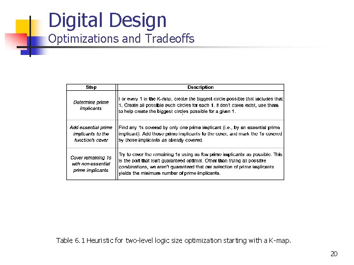
Digital Design Optimizations and Tradeoffs Table 6. 1 Heuristic for two-level logic size optimization starting with a K-map. 20

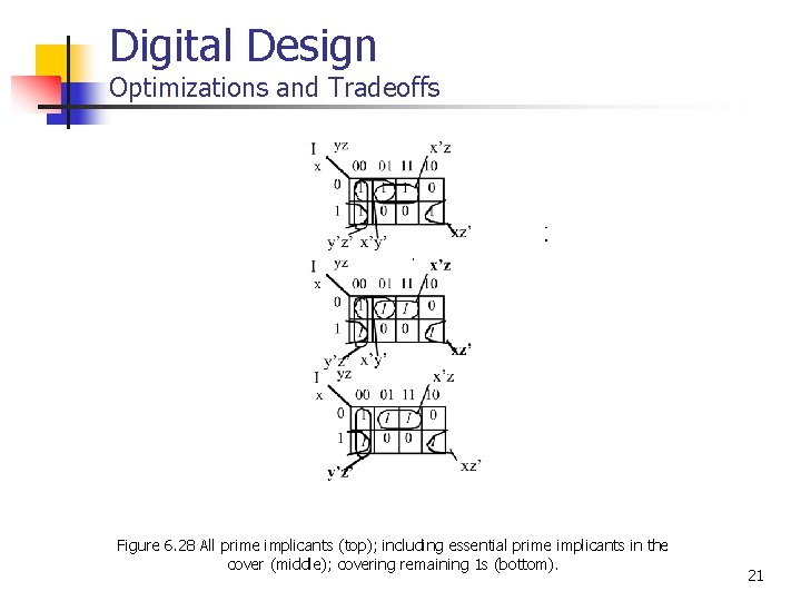
Digital Design Optimizations and Tradeoffs Figure 6. 28 All prime implicants (top); including essential prime implicants in the cover (middle); covering remaining 1 s (bottom). 21

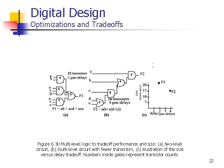
Digital Design Optimizations and Tradeoffs Figure 6. 30 Multi-level logic to tradeoff performance and size: (a) two-level circuit, (b) multi-level circuit with fewer transistors, (c) illustration of the size versus delay tradeoff. Numbers inside gates represent transistor counts. 22

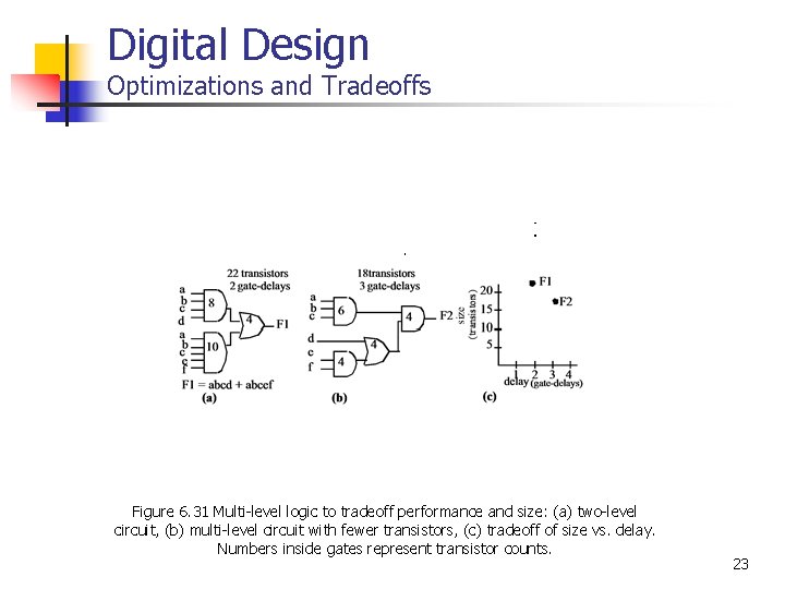
Digital Design Optimizations and Tradeoffs Figure 6. 31 Multi-level logic to tradeoff performance and size: (a) two-level circuit, (b) multi-level circuit with fewer transistors, (c) tradeoff of size vs. delay. Numbers inside gates represent transistor counts. 23

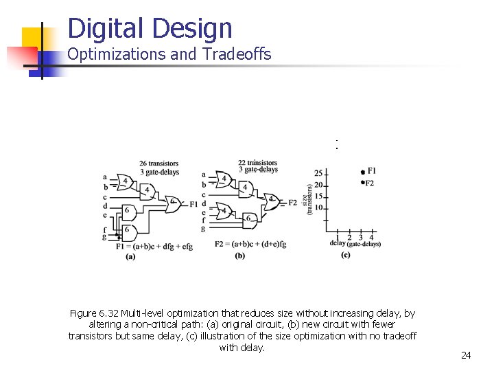
Digital Design Optimizations and Tradeoffs Figure 6. 32 Multi-level optimization that reduces size without increasing delay, by altering a non-critical path: (a) original circuit, (b) new circuit with fewer transistors but same delay, (c) illustration of the size optimization with no tradeoff with delay. 24

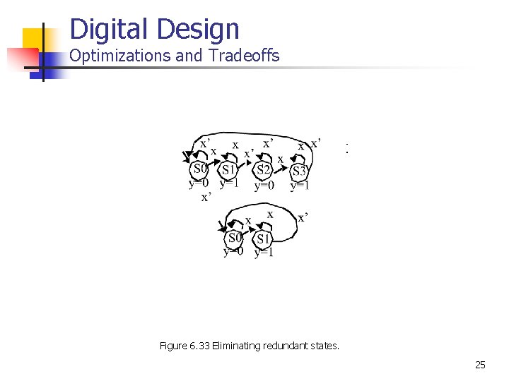
Digital Design Optimizations and Tradeoffs Figure 6. 33 Eliminating redundant states. 25

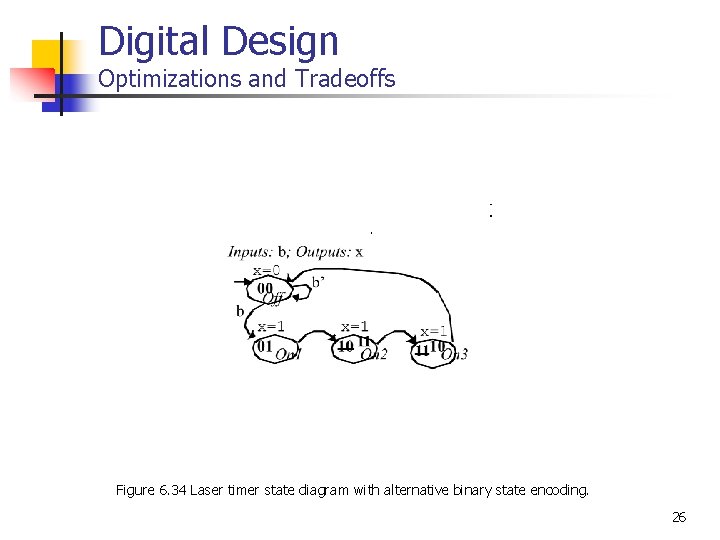
Digital Design Optimizations and Tradeoffs Figure 6. 34 Laser timer state diagram with alternative binary state encoding. 26

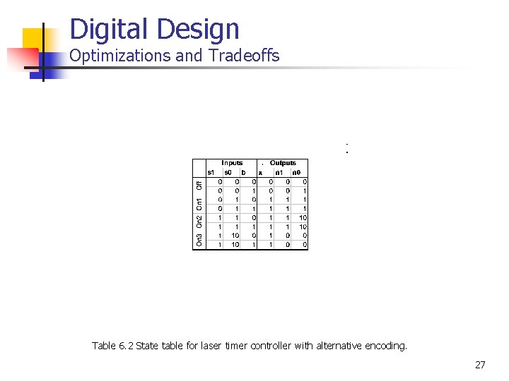
Digital Design Optimizations and Tradeoffs Table 6. 2 State table for laser timer controller with alternative encoding. 27

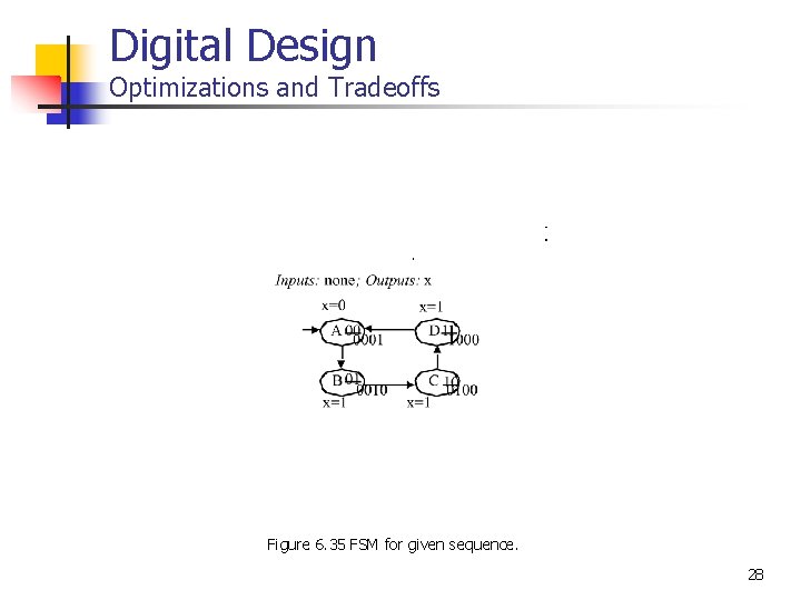
Digital Design Optimizations and Tradeoffs Figure 6. 35 FSM for given sequence. 28

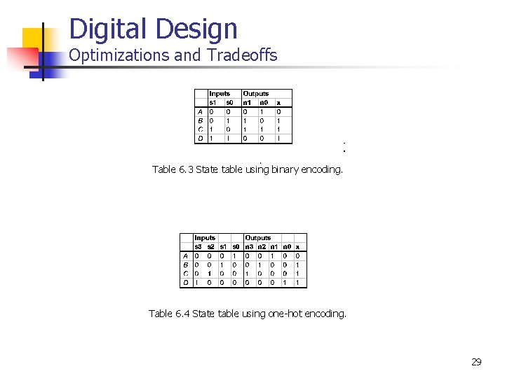
Digital Design Optimizations and Tradeoffs Table 6. 3 State table using binary encoding. Table 6. 4 State table using one-hot encoding. 29

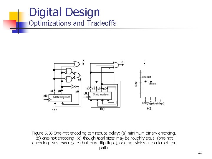
Digital Design Optimizations and Tradeoffs Figure 6. 36 One-hot encoding can reduce delay: (a) minimum binary encoding, (b) one-hot encoding, (c) though total sizes may be roughly equal (one-hot encoding uses fewer gates but more flip-flops), one-hot yields a shorter critical path. 30

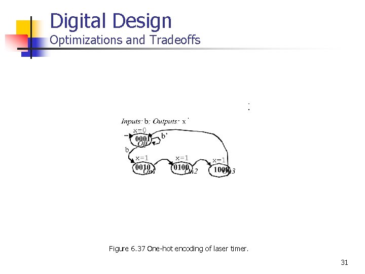
Digital Design Optimizations and Tradeoffs Figure 6. 37 One-hot encoding of laser timer. 31

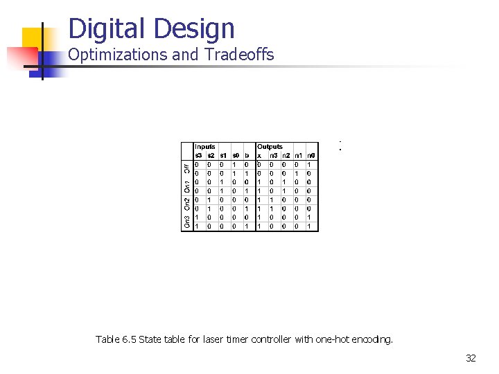
Digital Design Optimizations and Tradeoffs Table 6. 5 State table for laser timer controller with one-hot encoding. 32

Digital Design Optimizations and Tradeoffs Figure 6. 38 FSM for given sequence. 33

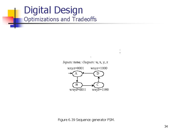
Digital Design Optimizations and Tradeoffs Figure 6. 39 Sequence generator FSM. 34

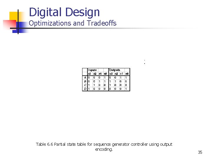
Digital Design Optimizations and Tradeoffs Table 6. 6 Partial state table for sequence generator controller using output encoding. 35

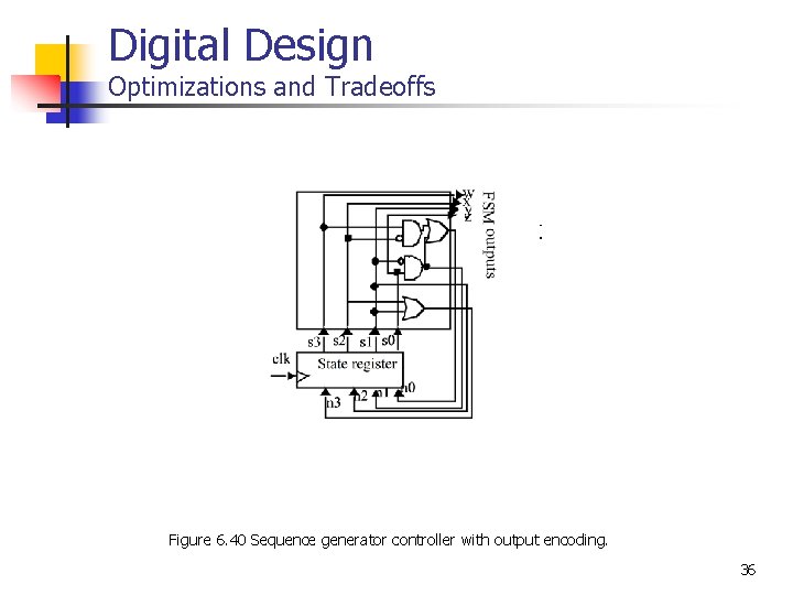
Digital Design Optimizations and Tradeoffs Figure 6. 40 Sequence generator controller with output encoding. 36

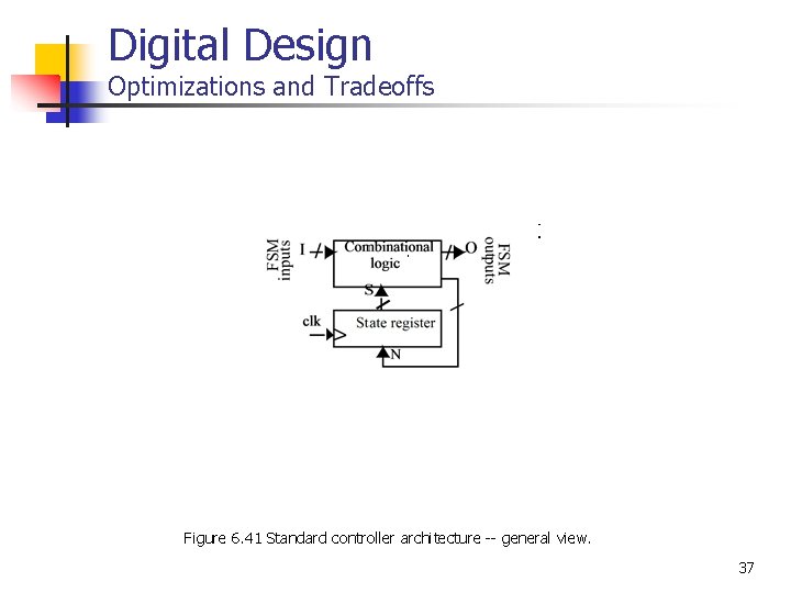
Digital Design Optimizations and Tradeoffs Figure 6. 41 Standard controller architecture -- general view. 37

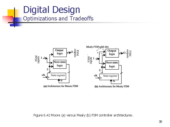
Digital Design Optimizations and Tradeoffs Figure 6. 42 Moore (a) versus Mealy (b) FSM controller architectures. 38

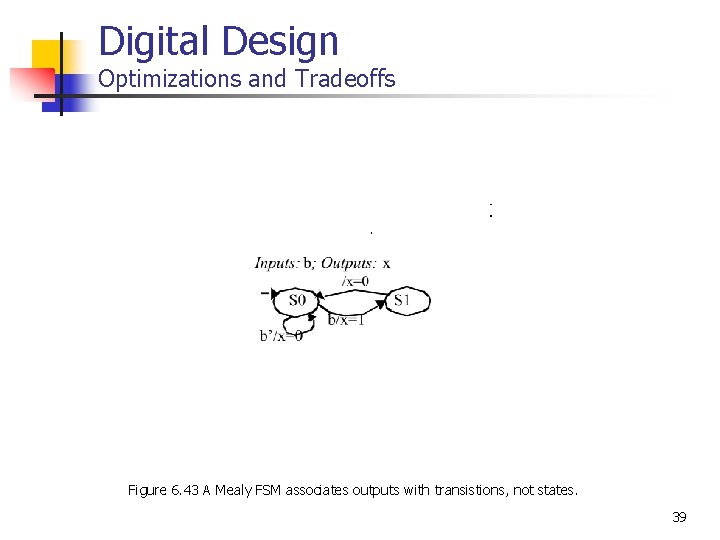
Digital Design Optimizations and Tradeoffs Figure 6. 43 A Mealy FSM associates outputs with transistions, not states. 39

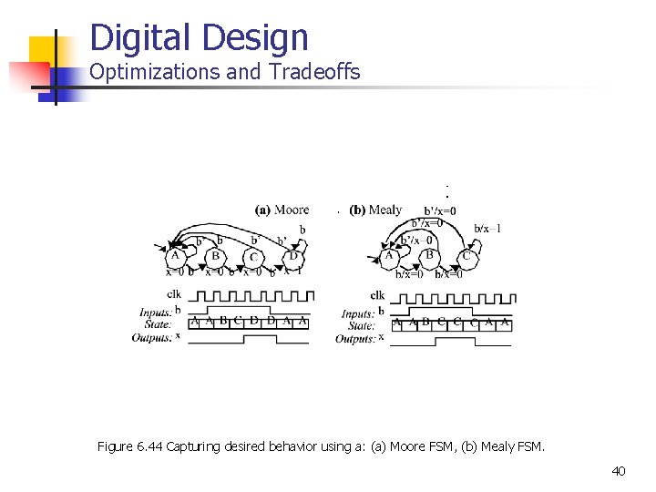
Digital Design Optimizations and Tradeoffs Figure 6. 44 Capturing desired behavior using a: (a) Moore FSM, (b) Mealy FSM. 40

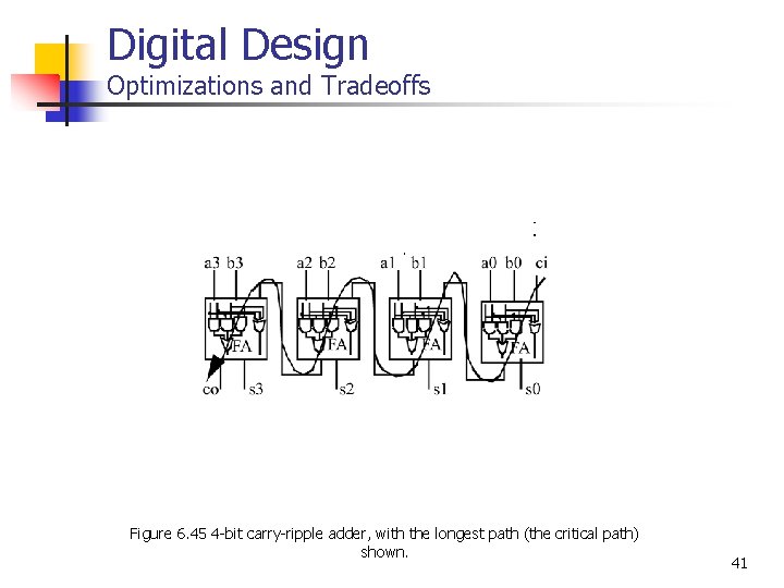
Digital Design Optimizations and Tradeoffs Figure 6. 45 4 -bit carry-ripple adder, with the longest path (the critical path) shown. 41

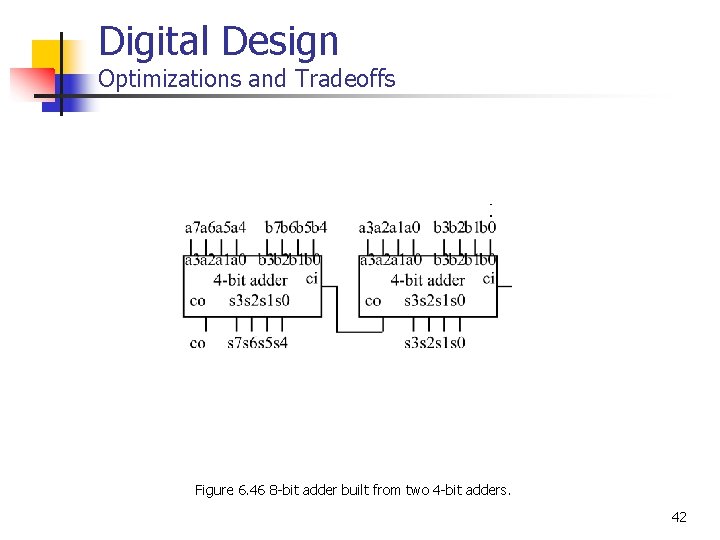
Digital Design Optimizations and Tradeoffs Figure 6. 46 8 -bit adder built from two 4 -bit adders. 42

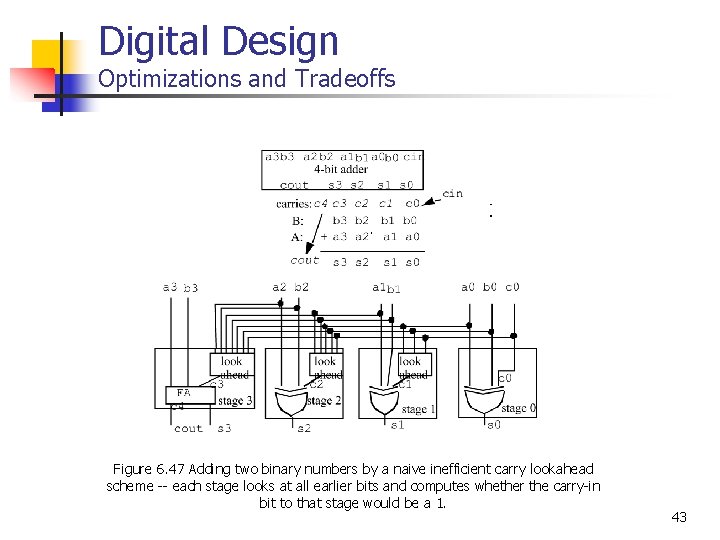
Digital Design Optimizations and Tradeoffs Figure 6. 47 Adding two binary numbers by a naive inefficient carry lookahead scheme -- each stage looks at all earlier bits and computes whether the carry-in bit to that stage would be a 1. 43

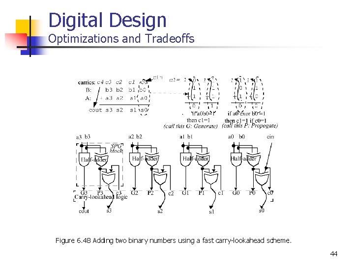
Digital Design Optimizations and Tradeoffs Figure 6. 48 Adding two binary numbers using a fast carry-lookahead scheme. 44

Digital Design Optimizations and Tradeoffs Figure 6. 48 Adding two binary numbers using a fast carry-lookahead scheme. (cont. ) 45

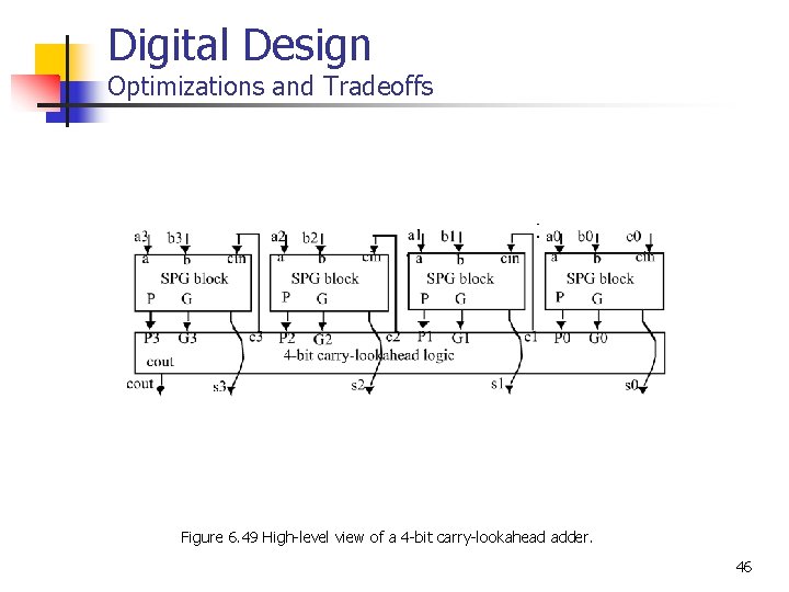
Digital Design Optimizations and Tradeoffs Figure 6. 49 High-level view of a 4 -bit carry-lookahead adder. 46

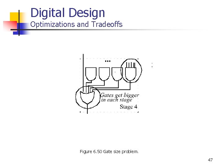
Digital Design Optimizations and Tradeoffs Figure 6. 50 Gate size problem. 47

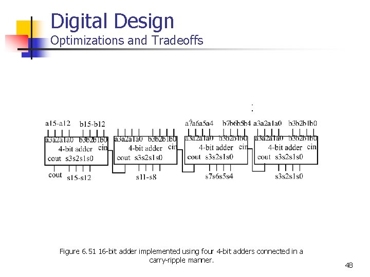
Digital Design Optimizations and Tradeoffs Figure 6. 51 16 -bit adder implemented using four 4 -bit adders connected in a carry-ripple manner. 48

Digital Design Optimizations and Tradeoffs Figure 6. 52 16 -bit adder implemented using four CLA 4 -bit adders and a second level of lookahead. 49

Digital Design Optimizations and Tradeoffs Figure 6. 53 Simplified view of multi-level carry-lookahead, showing tree structure, which enables fast addition with reasonable numbers and sizes of gates. Each level adds only two gate-delays. 50

Digital Design Optimizations and Tradeoffs Figure 6. 54 8 -bit adder block diagram (top left); carry-ripple implementation using two 4 -bit adders (top right); carry-select implementation using three 4 -bit adders (bottom). 51

Digital Design Optimizations and Tradeoffs Figure 6. 55 Adder tradeoffs. 52

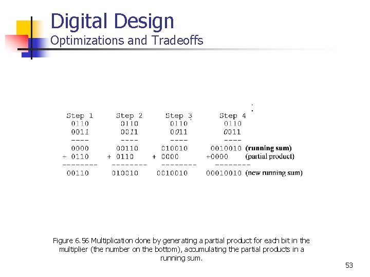
Digital Design Optimizations and Tradeoffs Figure 6. 56 Multiplication done by generating a partial product for each bit in the multiplier (the number on the bottom), accumulating the partial products in a running sum. 53

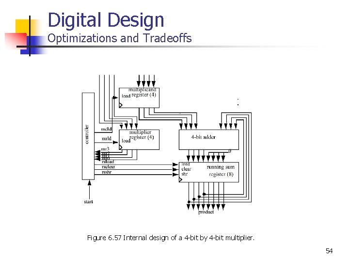
Digital Design Optimizations and Tradeoffs Figure 6. 57 Internal design of a 4 -bit by 4 -bit multiplier. 54

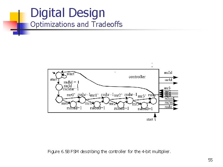
Digital Design Optimizations and Tradeoffs Figure 6. 58 FSM describing the controller for the 4 -bit multiplier. 55

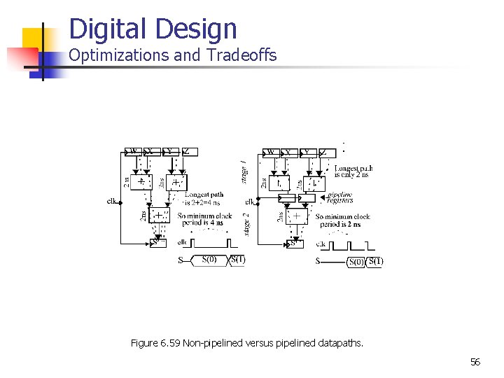
Digital Design Optimizations and Tradeoffs Figure 6. 59 Non-pipelined versus pipelined datapaths. 56

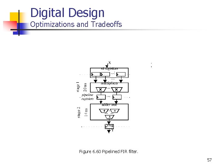
Digital Design Optimizations and Tradeoffs Figure 6. 60 Pipelined FIR filter. 57

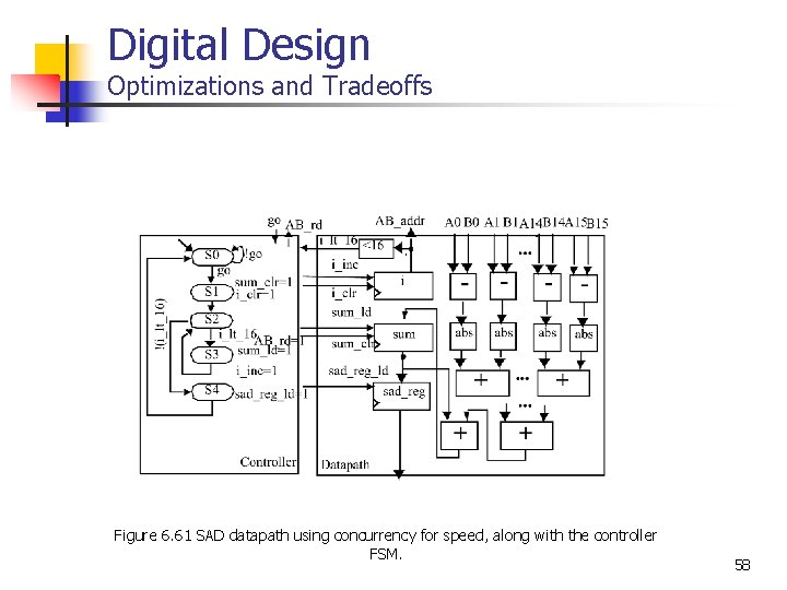
Digital Design Optimizations and Tradeoffs Figure 6. 61 SAD datapath using concurrency for speed, along with the controller FSM. 58

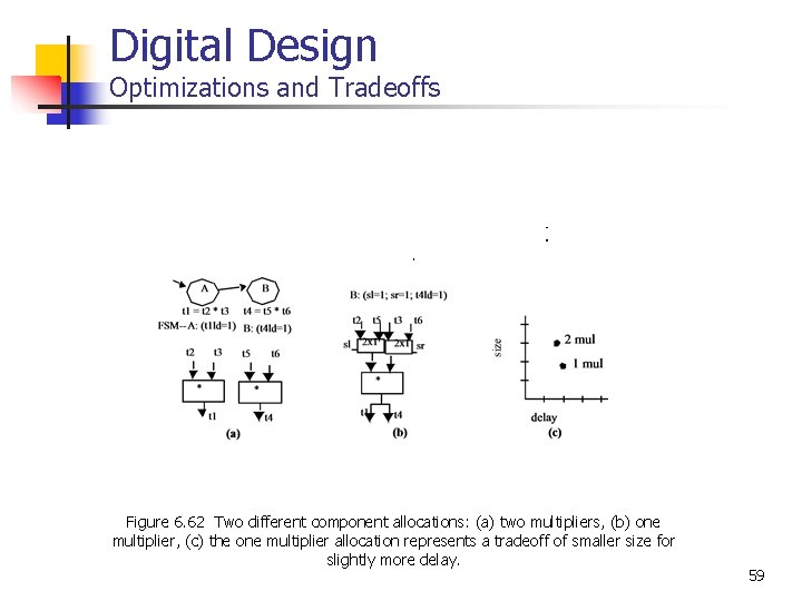
Digital Design Optimizations and Tradeoffs Figure 6. 62 Two different component allocations: (a) two multipliers, (b) one multiplier, (c) the one multiplier allocation represents a tradeoff of smaller size for slightly more delay. 59

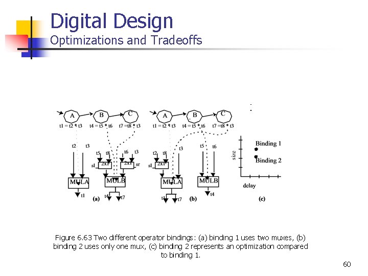
Digital Design Optimizations and Tradeoffs Figure 6. 63 Two different operator bindings: (a) binding 1 uses two muxes, (b) binding 2 uses only one mux, (c) binding 2 represents an optimization compared to binding 1. 60

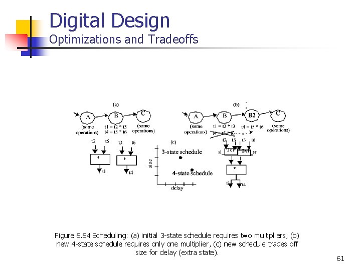
Digital Design Optimizations and Tradeoffs Figure 6. 64 Scheduling: (a) initial 3 -state schedule requires two multipliers, (b) new 4 -state schedule requires only one multiplier, (c) new schedule trades off size for delay (extra state). 61

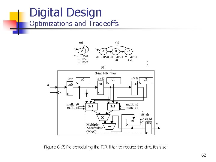
Digital Design Optimizations and Tradeoffs Figure 6. 65 Re-scheduling the FIR filter to reduce the circuit’s size. 62

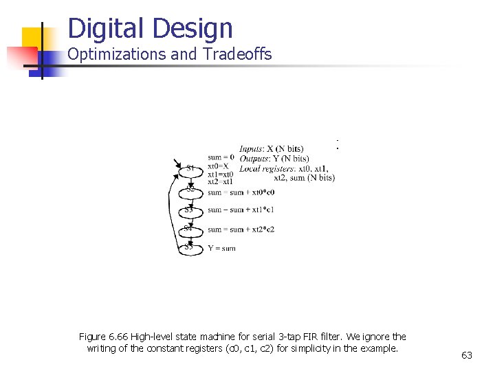
Digital Design Optimizations and Tradeoffs Figure 6. 66 High-level state machine for serial 3 -tap FIR filter. We ignore the writing of the constant registers (c 0, c 1, c 2) for simplicity in the example. 63

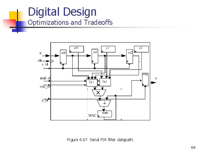
Digital Design Optimizations and Tradeoffs Figure 6. 67 Serial FIR filter datapath. 64

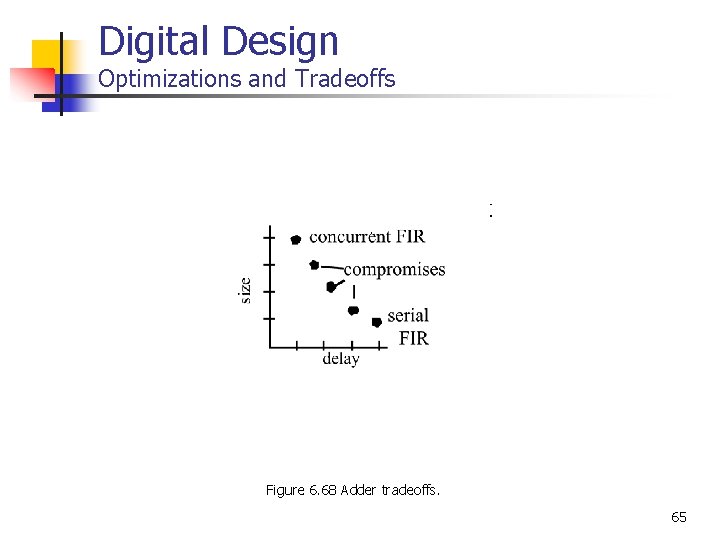
Digital Design Optimizations and Tradeoffs Figure 6. 68 Adder tradeoffs. 65

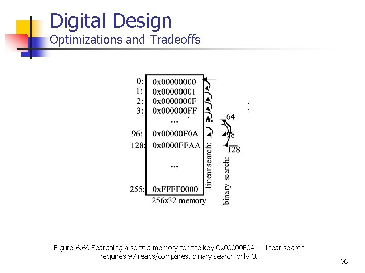
Digital Design Optimizations and Tradeoffs Figure 6. 69 Searching a sorted memory for the key 0 x 00000 F 0 A -- linear search requires 97 reads/compares, binary search only 3. 66

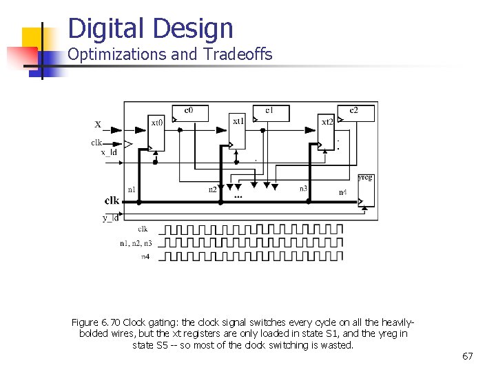
Digital Design Optimizations and Tradeoffs Figure 6. 70 Clock gating: the clock signal switches every cycle on all the heavilybolded wires, but the xt registers are only loaded in state S 1, and the yreg in state S 5 -- so most of the clock switching is wasted. 67

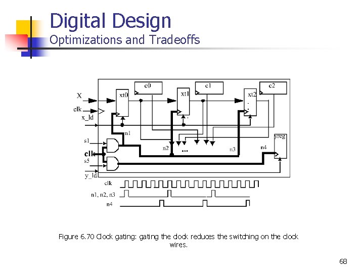
Digital Design Optimizations and Tradeoffs Figure 6. 70 Clock gating: gating the clock reduces the switching on the clock wires. 68

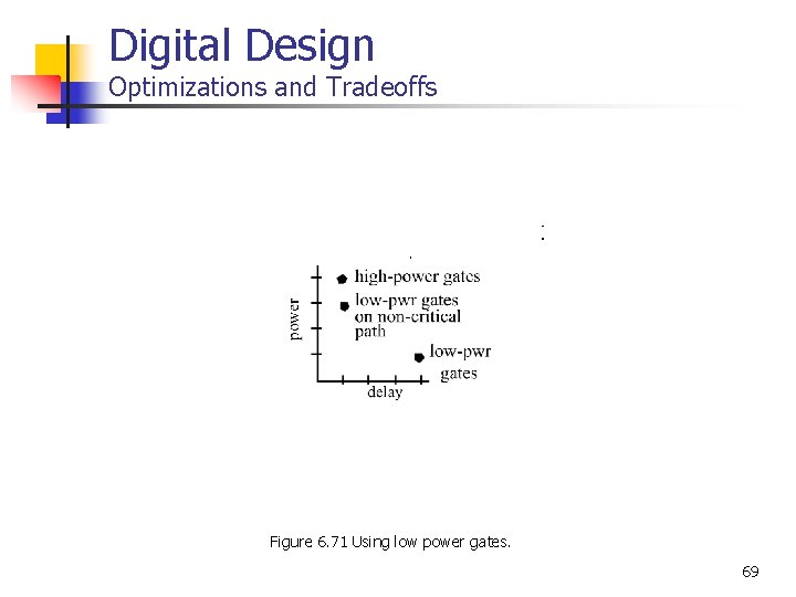
Digital Design Optimizations and Tradeoffs Figure 6. 71 Using low power gates. 69

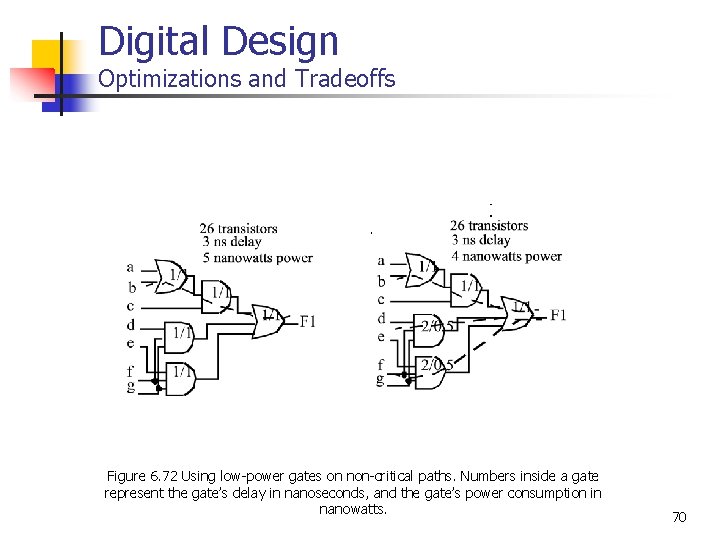
Digital Design Optimizations and Tradeoffs Figure 6. 72 Using low-power gates on non-critical paths. Numbers inside a gate represent the gate’s delay in nanoseconds, and the gate’s power consumption in nanowatts. 70