Digital Design and Synthesis with Verilog HDL Eli

![Anatomy of the Verilog HDL • Example of a function [7: 0] func; input Anatomy of the Verilog HDL • Example of a function [7: 0] func; input](https://slidetodoc.com/presentation_image_h/32eb477bdaa491ffad3e4061f2c67e90/image-26.jpg)
- Slides: 40

Digital Design and Synthesis with Verilog HDL Eli Sternheim, Ph. D. inter. HDL, Inc. Rajvir Singh inter. HDL, Inc. Rajeev Madhavan Cadence Design System, Inc. Yatin Trivedi YT Associates 1

Chapter 1 • Why hardware description languages? • Evolutionary trends in design methods. • The use of hardware description languages (HDLs) for logic design has greatly expanded in the last few years. • Engineering managers no longer face the dilemma of whether to design with an HDL or not. 2

Designing with Verilog HDL • Verilog HDL is simple and elegant. • It provides constructs to describe hardware elements in a succinet and readable form. • A comparable description, for example in VHDL, can be twice as long as a Verilog description. 3

Designing with Verilog HDL • In Verilog, a designer needs to learn only one language for all aspects of logic design. • Simulation of a design, at least, requires functional models, hierarchical structures, test vectors, and man/machine interaction. • In Verilog, all of these are achieved by one language. • Almost every statement that can be written in procedural code can also be issued in an interactive session from the terminal. 4

Designing with Verilog HDL • Verilog is not only concise and uniform, but also is easy to learn. • It is very similar to the C programming language. • Since C is one of the most widely used programming languages, most designers should be familiar with it and may, therefore, find it easy to learn Verilog. 5

Chapter 2 • Anatomy of the Verilog HDL • In this chapter we introduce the Verilog hardware description language through a sequence of examples. • A more complete specification of the language can be found in the ”Language Reference Manual” and in the ”Condensed Reference Manual” in Appendix A. 6

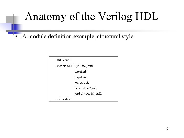
Anatomy of the Verilog HDL • A module definition example, structural style. //structural module AND 2 (in 1, in 2, out); input in 1; input in 2; output out; wire in 1, in 2, out; and u 1 (out, in 1, in 2); endmodule 7

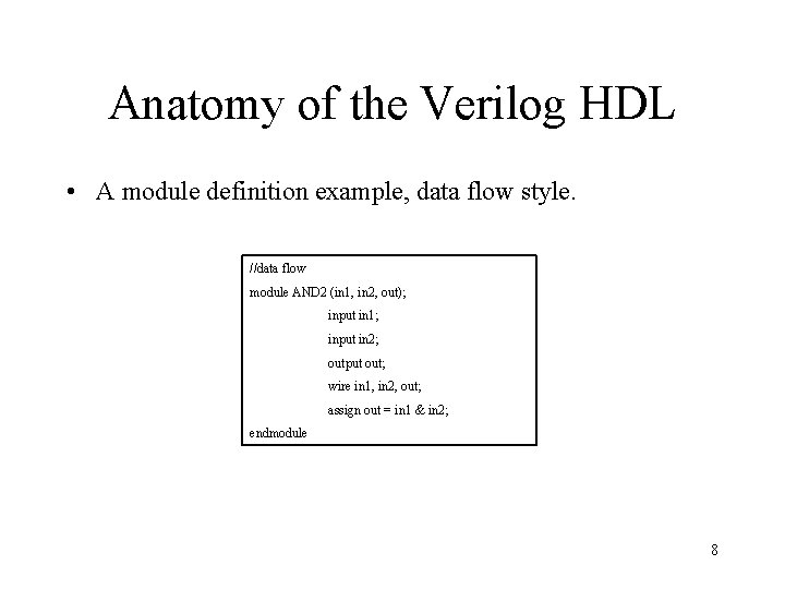
Anatomy of the Verilog HDL • A module definition example, data flow style. //data flow module AND 2 (in 1, in 2, out); input in 1; input in 2; output out; wire in 1, in 2, out; assign out = in 1 & in 2; endmodule 8

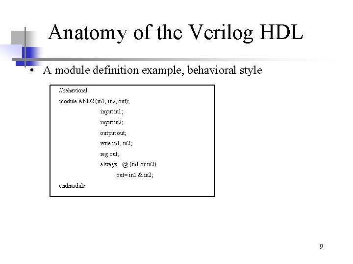
Anatomy of the Verilog HDL • A module definition example, behavioral style //behavioral module AND 2 (in 1, in 2, out); input in 1; input in 2; output out; wire in 1, in 2; reg out; always @ (in 1 or in 2) out= in 1 & in 2; endmodule 9

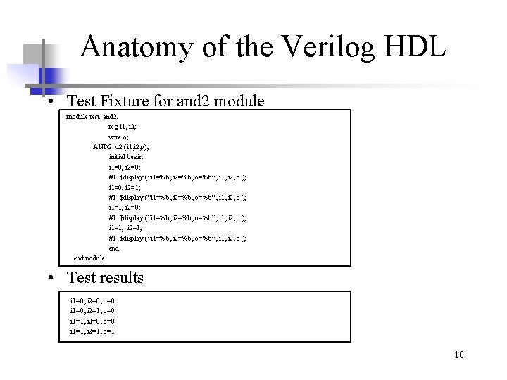
Anatomy of the Verilog HDL • Test Fixture for and 2 module test_and 2; reg i 1, i 2; wire o; AND 2 u 2 (i 1, i 2, o); initial begin i 1=0; i 2=0; #1 $display (”i 1=%b, i 2=%b, o=%b”, i 1, i 2, o ); i 1=0; i 2=1; #1 $display (”i 1=%b, i 2=%b, o=%b”, i 1, i 2, o ); i 1=1; i 2=0; #1 $display (”i 1=%b, i 2=%b, o=%b”, i 1, i 2, o ); i 1=1; i 2=1; #1 $display (”i 1=%b, i 2=%b, o=%b”, i 1, i 2, o ); endmodule • Test results i 1=0, i 2=0, o=0 i 1=0, i 2=1, o=0 i 1=1, i 2=0, o=0 i 1=1, i 2=1, o=1 10

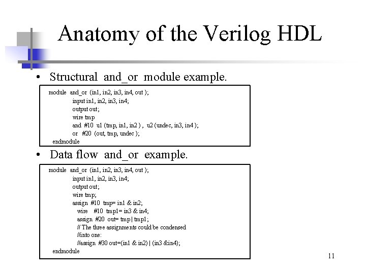
Anatomy of the Verilog HDL • Structural and_or module example. module and_or (in 1, in 2, in 3, in 4, out ); input in 1, in 2, in 3, in 4; output out; wire tmp and #10 u 1 (tmp, in 1, in 2 ) , u 2 (undec, in 3, in 4 ); or #20 (out, tmp, undec ); endmodule • Data flow and_or example. module and_or (in 1, in 2, in 3, in 4, out ); input in 1, in 2, in 3, in 4; output out; wire tmp; assign #10 tmp= in 1 & in 2; wire #10 tmp 1= in 3 & in 4; assign #20 out= tmp | tmp 1; // The three assignments could be condensed //into one: //assign #30 out=(in 1 & in 2) | (in 3 &in 4); endmodule 11

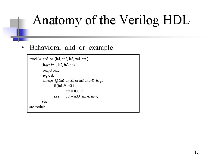
Anatomy of the Verilog HDL • Behavioral and_or example. module and_or (in 1, in 2, in 3, in 4, out ); input in 1, in 2, in 3, in 4; output out; reg out; always @ (in 1 or in 2 or in 3 or in 4) begin if (in 1 & in 2 ) out = #30 1; else out = #30 (in 3 & in 4); endmodule 12

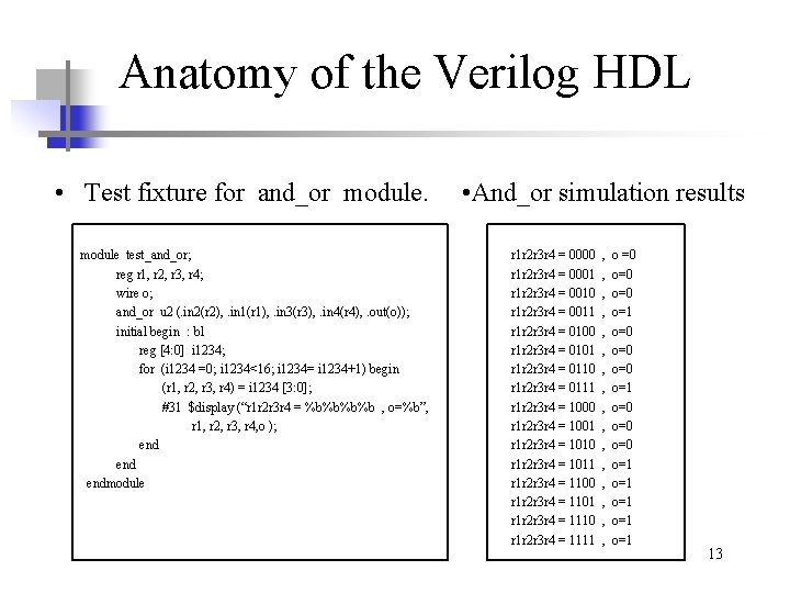
Anatomy of the Verilog HDL • Test fixture for and_or module test_and_or; reg r 1, r 2, r 3, r 4; wire o; and_or u 2 (. in 2(r 2), . in 1(r 1), . in 3(r 3), . in 4(r 4), . out(o)); initial begin : bl reg [4: 0] i 1234; for (i 1234 =0; i 1234<16; i 1234= i 1234+1) begin (r 1, r 2, r 3, r 4) = i 1234 [3: 0]; #31 $display (“r 1 r 2 r 3 r 4 = %b%b , o=%b”, r 1, r 2, r 3, r 4, o ); end endmodule • And_or simulation results r 1 r 2 r 3 r 4 = 0000 r 1 r 2 r 3 r 4 = 0001 r 1 r 2 r 3 r 4 = 0010 r 1 r 2 r 3 r 4 = 0011 r 1 r 2 r 3 r 4 = 0100 r 1 r 2 r 3 r 4 = 0101 r 1 r 2 r 3 r 4 = 0110 r 1 r 2 r 3 r 4 = 0111 r 1 r 2 r 3 r 4 = 1000 r 1 r 2 r 3 r 4 = 1001 r 1 r 2 r 3 r 4 = 1010 r 1 r 2 r 3 r 4 = 1011 r 1 r 2 r 3 r 4 = 1100 r 1 r 2 r 3 r 4 = 1101 r 1 r 2 r 3 r 4 = 1110 r 1 r 2 r 3 r 4 = 1111 , , , , o =0 o=0 o=0 o=1 o=1 o=1 13

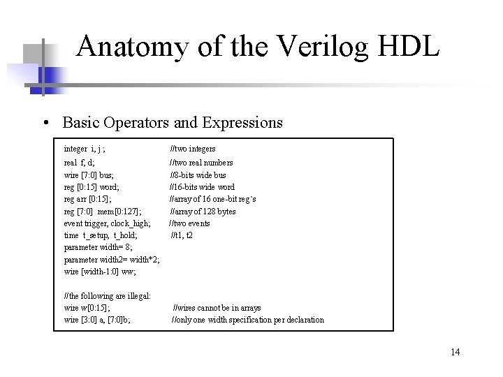
Anatomy of the Verilog HDL • Basic Operators and Expressions integer i, j ; //two integers real f, d; wire [7: 0] bus; reg [0: 15] word; reg arr [0: 15]; reg [7: 0] mem[0: 127]; event trigger, clock_high; time t_setup, t_hold; parameter width= 8; parameter width 2= width*2; wire [width-1: 0] ww; //two real numbers //8 -bits wide bus //16 -bits wide word //array of 16 one-bit reg`s //array of 128 bytes //two events //t 1, t 2 //the following are illegal: wire w[0: 15]; wire [3: 0] a, [7: 0]b; //wires cannot be in arrays //only one width specification per declaration 14

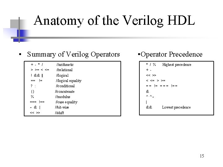
Anatomy of the Verilog HDL • Summary of Verilog Operators + - * / > >= < <= ! && || == != ? : {} % === !== ~ & | << >> //arithmetic //relational //logical equality //conditional //concatenate //modulus //case equality //bit-wise //shift • Operator Precedence * / % Highest precedence + << >> < <= > >= = = != = & ^ ^~ | && Lowest precedence 15

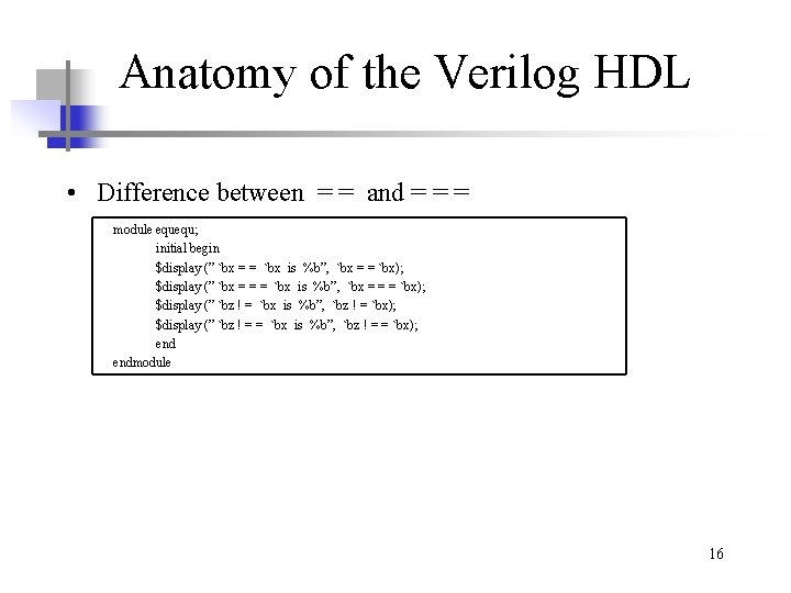
Anatomy of the Verilog HDL • Difference between = = and = = = module equequ; initial begin $display (” `bx = = `bx is %b”, `bx = = `bx); $display (” `bx = = = `bx is %b”, `bx = = = `bx); $display (” `bz ! = `bx is %b”, `bz ! = `bx); $display (” `bz ! = = `bx is %b”, `bz ! = = `bx); endmodule 16

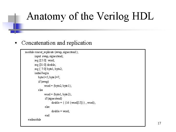
Anatomy of the Verilog HDL • Concatenation and replication module concat_replicate (swap, signextend ); input swap, signextend; reg [15: 0] word; reg [31: 0] double; reg [ 7: 0] byte 1, byte 2; initial begin byte 1=5; byte 2=7; if (swap) word = {byte 2, byte 1}; else word = {byte 1, byte 2}; if (signextend) double = { {16 {word[15]}} , word}; else double = word; endmodule 17

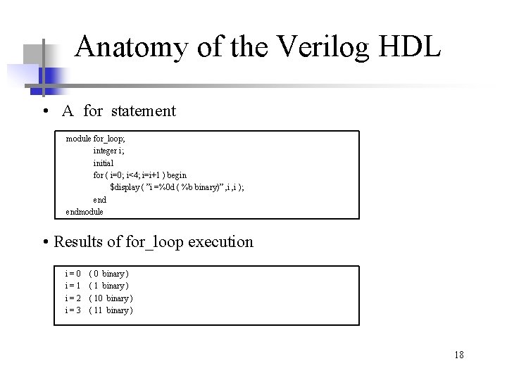
Anatomy of the Verilog HDL • A for statement module for_loop; integer i; initial for ( i=0; i<4; i=i+1 ) begin $display ( ”i =%0 d ( %b binary)” , i ); endmodule • Results of for_loop execution i=0 i=1 i=2 i=3 ( 0 binary ) ( 10 binary ) ( 11 binary ) 18

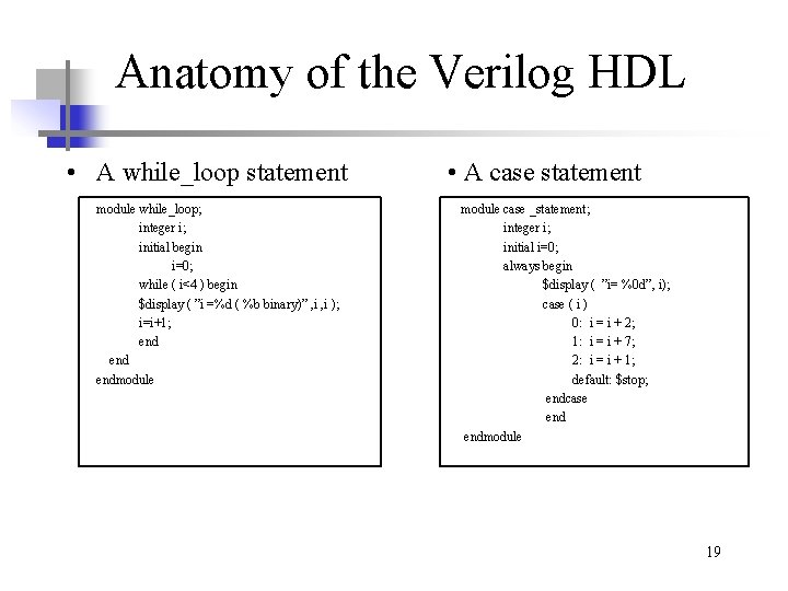
Anatomy of the Verilog HDL • A while_loop statement module while_loop; integer i; initial begin i=0; while ( i<4 ) begin $display ( ”i =%d ( %b binary)” , i ); i=i+1; end endmodule • A case statement module case _statement; integer i; initial i=0; always begin $display ( ”i= %0 d”, i); case ( i ) 0: i = i + 2; 1: i = i + 7; 2: i = i + 1; default: $stop; endcase endmodule 19

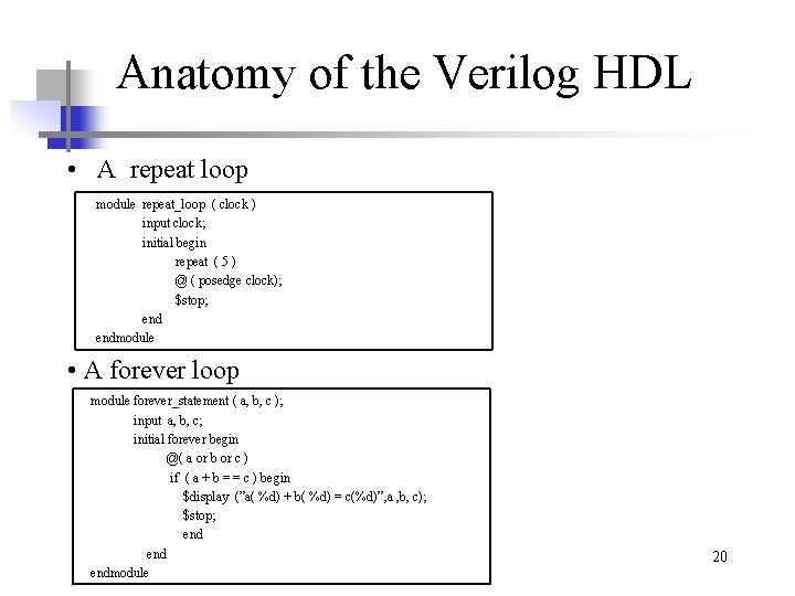
Anatomy of the Verilog HDL • A repeat loop module repeat_loop ( clock ) input clock; initial begin repeat ( 5 ) @ ( posedge clock); $stop; endmodule • A forever loop module forever_statement ( a, b, c ); input a, b, c; initial forever begin @( a or b or c ) if ( a + b = = c ) begin $display (”a( %d) + b( %d) = c(%d)”, a , b, c); $stop; end endmodule 20

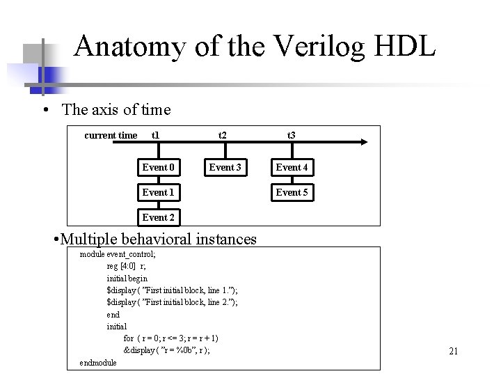
Anatomy of the Verilog HDL • The axis of time current time t 1 t 2 t 3 Event 0 Event 3 Event 4 Event 1 Event 5 Event 2 • Multiple behavioral instances module event_control; reg [4: 0] r; initial begin $display ( ”First initial block, line 1. ”); $display ( ”First initial block, line 2. ”); end initial for ( r = 0; r <= 3; r = r + 1) &display ( ”r = %0 b”, r ); endmodule 21

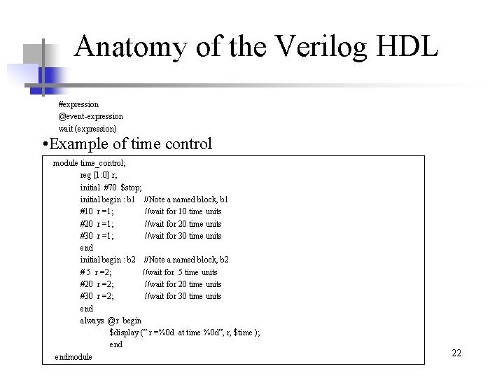
Anatomy of the Verilog HDL #expression @event-expression wait (expression) • Example of time control module time_control; reg [1: 0] r; initial #70 $stop; initial begin : b 1 //Note a named block, b 1 #10 r =1; //wait for 10 time units #20 r =1; //wait for 20 time units #30 r =1; //wait for 30 time units end initial begin : b 2 //Note a named block, b 2 # 5 r =2; //wait for 5 time units #20 r =2; //wait for 20 time units #30 r =2; //wait for 30 time units end always @r begin $display (” r =%0 d at time %0 d”, r, $time ); endmodule 22

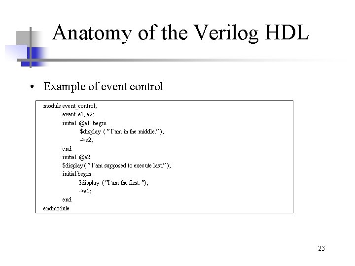
Anatomy of the Verilog HDL • Example of event control module event_control; event e 1, e 2; initial @e 1 begin $display ( ” I`am in the middle. ” ); ->e 2; end initial @e 2 $display ( ” I`am supposed to execute last. ” ); initial begin $display ( ”I`am the first. ”); ->e 1; endmodule 23

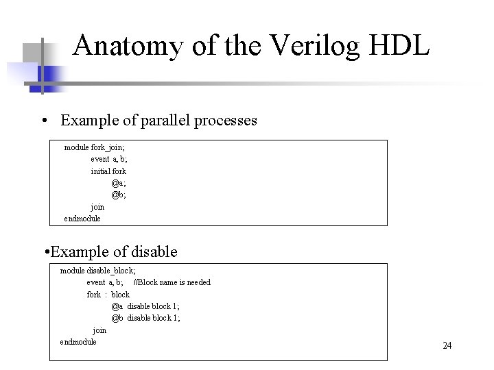
Anatomy of the Verilog HDL • Example of parallel processes module fork_join; event a, b; initial fork @a; @b; join endmodule • Example of disable module disable_block; event a, b; //Block name is needed fork : block @a disable block 1; @b disable block 1; join endmodule 24

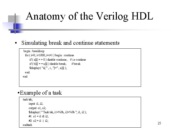
Anatomy of the Verilog HDL • Simulating break and continue statements begin : breakloop for ( i=0; i<1000; i=i+1 ) begin : continue if ( a[i] = = 0 ) disable continue; // i. e continue if ( b[i] = = a[i] ) disable break; // break $display ( ”a[ ” , i , ”]=” , a[i] ); end • Example of a task tsk; input i 1, i 2; output o 1, o 2; $display ( ” Task tsk, i 1=%0 b, i 2=%0 b ”, i 1, i 2 ); #1 o 1 = i 1 & i 2; #2 o 2 = i 1 | i 2; endtask 25
![Anatomy of the Verilog HDL Example of a function 7 0 func input Anatomy of the Verilog HDL • Example of a function [7: 0] func; input](https://slidetodoc.com/presentation_image_h/32eb477bdaa491ffad3e4061f2c67e90/image-26.jpg)
Anatomy of the Verilog HDL • Example of a function [7: 0] func; input i 1; integer i 1; reg [7: 0] rg; begin rg = 1; for ( i = 1; i <= i 1; i = i +1 ) rg =rg + 1; func = rg; endfunction 26

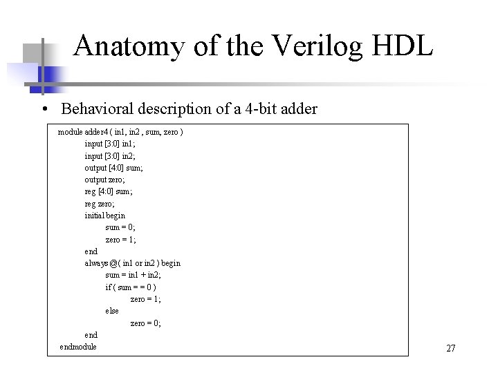
Anatomy of the Verilog HDL • Behavioral description of a 4 -bit adder module adder 4 ( in 1, in 2 , sum, zero ) input [3: 0] in 1; input [3: 0] in 2; output [4: 0] sum; output zero; reg [4: 0] sum; reg zero; initial begin sum = 0; zero = 1; end always @( in 1 or in 2 ) begin sum = in 1 + in 2; if ( sum = = 0 ) zero = 1; else zero = 0; endmodule 27

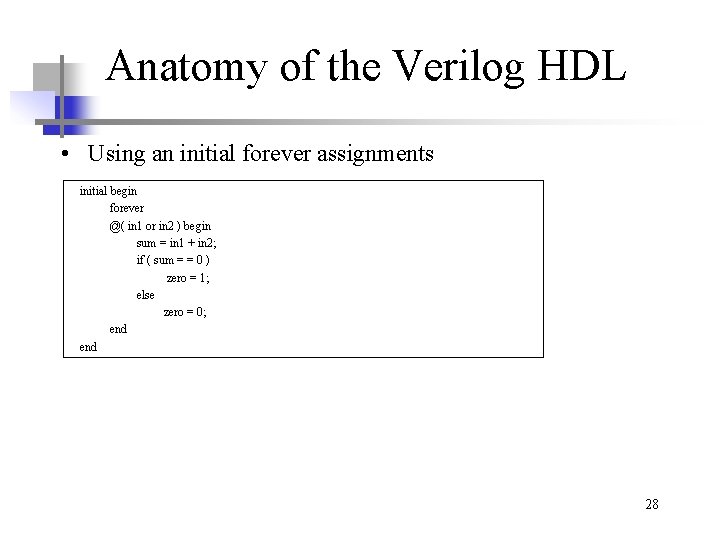
Anatomy of the Verilog HDL • Using an initial forever assignments initial begin forever @( in 1 or in 2 ) begin sum = in 1 + in 2; if ( sum = = 0 ) zero = 1; else zero = 0; end 28

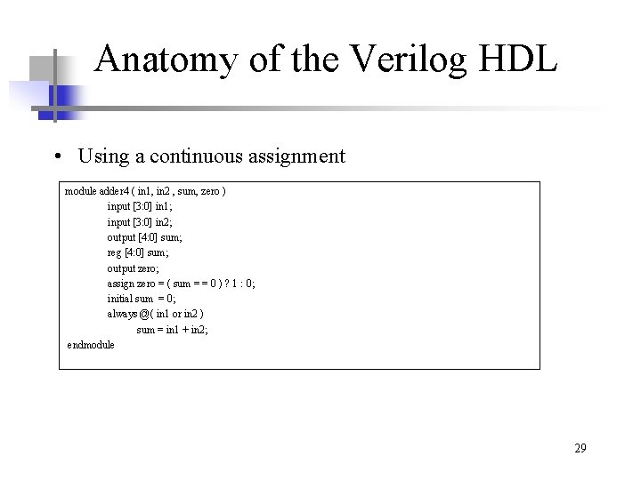
Anatomy of the Verilog HDL • Using a continuous assignment module adder 4 ( in 1, in 2 , sum, zero ) input [3: 0] in 1; input [3: 0] in 2; output [4: 0] sum; reg [4: 0] sum; output zero; assign zero = ( sum = = 0 ) ? 1 : 0; initial sum = 0; always @( in 1 or in 2 ) sum = in 1 + in 2; endmodule 29

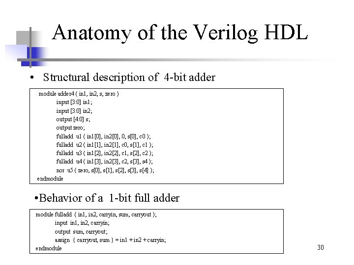
Anatomy of the Verilog HDL • Structural description of 4 -bit adder module adder 4 ( in 1, in 2, s, zero ) input [3: 0] in 1; input [3: 0] in 2; output [4: 0] s; output zero; fulladd u 1 ( in 1[0], in 2[0], 0, s[0], c 0 ); fulladd u 2 ( in 1[1], in 2[1], c 0, s[1], c 1 ); fulladd u 3 ( in 1[2], in 2[2], c 1, s[2], c 2 ); fulladd u 4 ( in 1[3], in 2[3], c 2, s[3], s 4 ); nor u 5 ( zero, s[0], s[1], s[2], s[3], s[4] ); endmodule • Behavior of a 1 -bit full adder module fulladd ( in 1, in 2, carryin, sum, carryout ); input in 1, in 2, carryin; output sum, carryout; assign { carryout, sum } = in 1 + in 2 + carryin; endmodule 30

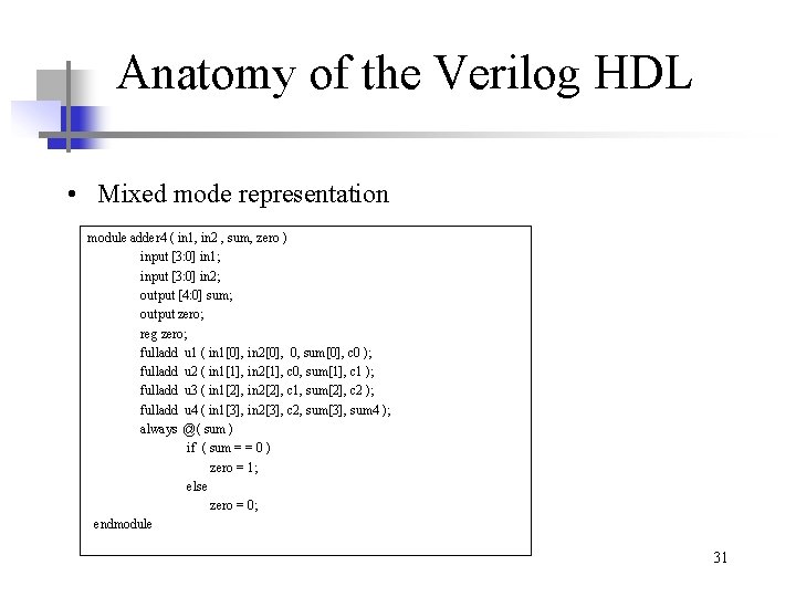
Anatomy of the Verilog HDL • Mixed mode representation module adder 4 ( in 1, in 2 , sum, zero ) input [3: 0] in 1; input [3: 0] in 2; output [4: 0] sum; output zero; reg zero; fulladd u 1 ( in 1[0], in 2[0], 0, sum[0], c 0 ); fulladd u 2 ( in 1[1], in 2[1], c 0, sum[1], c 1 ); fulladd u 3 ( in 1[2], in 2[2], c 1, sum[2], c 2 ); fulladd u 4 ( in 1[3], in 2[3], c 2, sum[3], sum 4 ); always @( sum ) if ( sum = = 0 ) zero = 1; else zero = 0; endmodule 31

Chapter 3 • Modeling a Pipelined Processor • In this chapter we take the specification of a 32 -bit processor and develop a functional model for it through various stages of successive refinement. • First we implement an instruction set model, then we describe a register transfer level (RTL) model. • In the next chapter we arrive at a structural model that maps the processor to various building blocks. • In the process, we explain modeling of such concepts as pipelining, concurrency, instruction execution, functional partitioning, and creation of test vectors. 32

Modeling a Pipelined Processor • The emphasis here is on the process of modeling as opposed to describing the architecture of a processor. • It is not our intention to explain the detailed functionality of any commercial microprocessor or architecture. • Some discussion on processor architecture is presented to explain the concepts and process of modeling. 33

Chapter 4 • Modeling System Blocks • In the previous chapter we saw how to model a processor at the instruction set level and its function at the behavioral level. • In this chapter we present a structural model of the SISC processor and show to model its various building blocks. • We begin with the block diagram of the SISC processor and present its corresponding structural model to show the interconnections of its building blocks. • In subsequent sections we develop functional models for these blocks, namely, the datapath, the memory elements, the clock generator and the control unit. 34

Chapter 5 • Modeling Cache Memories • In this chapter we examine the process of designing a simple cache system in Verilog HDL. • The description can be synthesized to obtain a gate level implementation. • At the end of this chapter we consider ways to improve the basic design. 35

Modeling Cache Memories • A cache in a computer system is a small, fast, local memory that stores data from the most frequently accessed addresses. • The cache is always small compared to main memory because cache RAMs are more expensive then the slower dynamic RAMs used for main memory. • As a result, only a small portion of the main memory can be stored in the cache. • The efficiency of a cache is measured by the cache hit ratio, i. e. , the number of times data is accessed from the cache over the total number of memory accesses. • Typical hit ratios are in the range of eighty to one hundred percent. 36

Chapter 6 • Modeling Asynchronous I/O: UART • In this chapter we present an example of modeling an asynchronous peripheral device, a dual Universal Asynchronous Receiver Transmitter (UART) chip. • We develop two models of the chip. • The first model is a high-level abstraction which describes the functionality of the chip and emphasizes simplicity, readability and ease of change. • The second model is oriented toward gate-level implementation. • This model is partitioned so that a logic synthesizer can be used to automatically implement the chip with library components. 37

Chapter 7 • Verilog HDL for Synthesis • In the previous chapters we introduced Verilog HDL and showed how it can be used in different ways to support top-down hierarchical design. • In this chapter we cover the basics of synthesis, discuss how Verilog may be used for synthesis and describe how modeling for synthesis affects the coding style, the design organization and partitioning. 38

Chapter 8 • Modeling a Floppy Disk Subsystem • In this chapter we provide a complete example of a floppy disk subsystem (FDS) model in Verilog. • Such a model may be needed when you perform a full system simulation and want to simulate the execution of code which accesses the disk. • The FDS model would typically be used to perform a full functional simulation during the development of a CPU board. • This example demonstrates the modeling of asynchronous systems, I/O buses, timing constraints, and other techniques of writing large models. 39

Chapter 9 • Useful Modeling and Debugging Techniques • Learning to design and simulate in Verilog is more then just learning the syntax and semantics of the language. • As in every learning process, the best way to learn is by doing. • As you start using the language, you will develop your own style of design, and you will discover techniques for modeling in Verilog. • In this chapter we present some tips and techniques that we hope will help you in developing your own techniques on the way to mastering Verilog. 40