TopDown Verilog HDL RTL module muxtwo out a
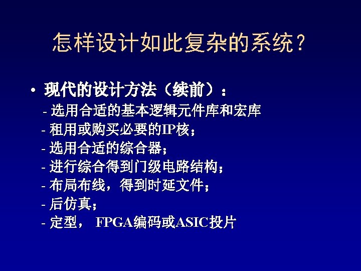
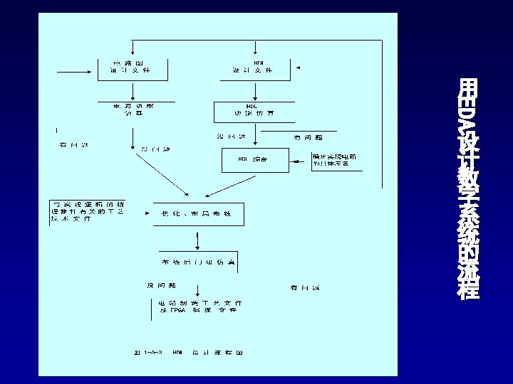
- Slides: 82
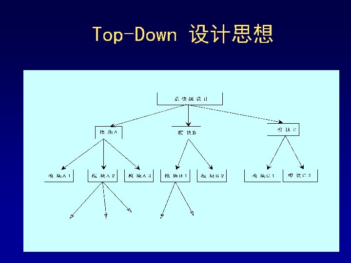
Top-Down 设计思想
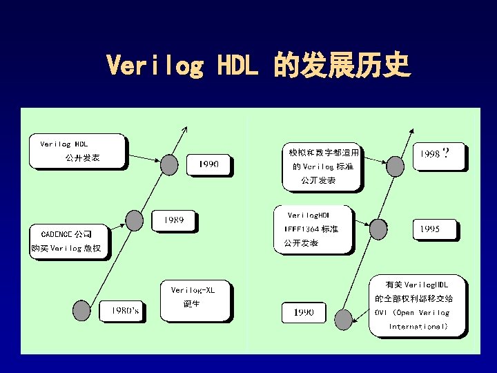
Verilog HDL 的发展历史
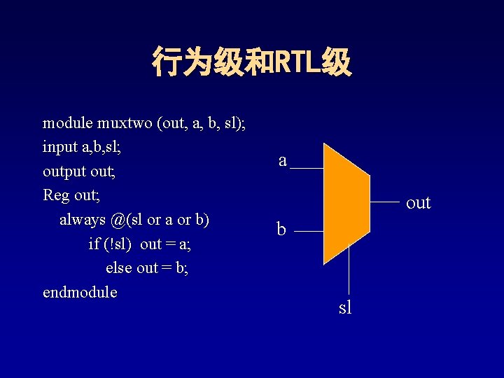
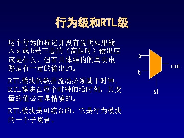
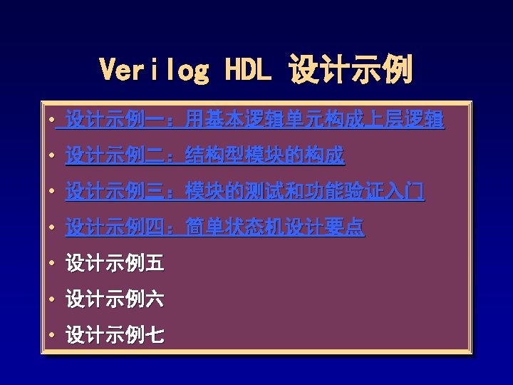
行为级和RTL级 module muxtwo (out, a, b, sl); input a, b, sl; output out; Reg out; always @(sl or a or b) if (!sl) out = a; else out = b; endmodule a out b sl
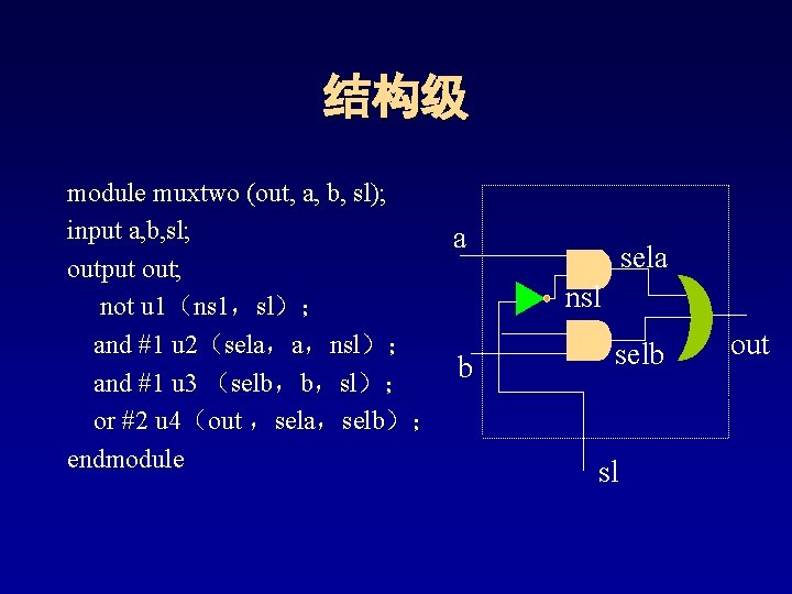
结构级 module muxtwo (out, a, b, sl); input a, b, sl; a output out; not u 1(ns 1,sl); and #1 u 2(sela,a,nsl); b and #1 u 3 (selb,b,sl); or #2 u 4(out ,sela,selb); endmodule sela nsl selb sl out
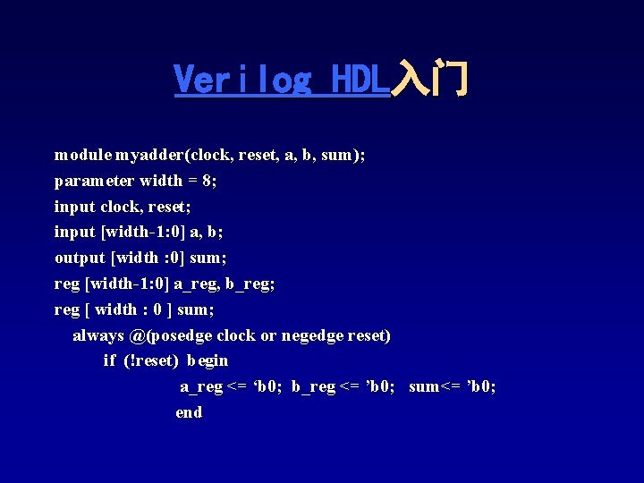
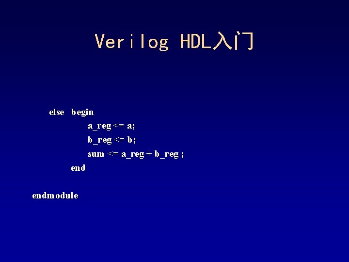
Verilog HDL入门 module myadder(clock, reset, a, b, sum); parameter width = 8; input clock, reset; input [width-1: 0] a, b; output [width : 0] sum; reg [width-1: 0] a_reg, b_reg; reg [ width : 0 ] sum; always @(posedge clock or negedge reset) if (!reset) begin a_reg <= ‘b 0; b_reg <= ’b 0; sum<= ’b 0; end
Verilog HDL入门 else begin a_reg <= a; b_reg <= b; sum <= a_reg + b_reg ; endmodule
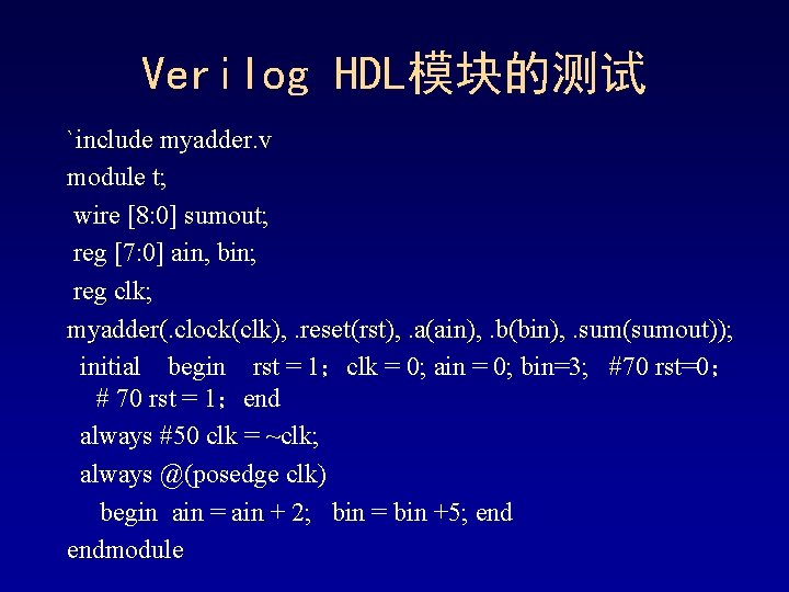
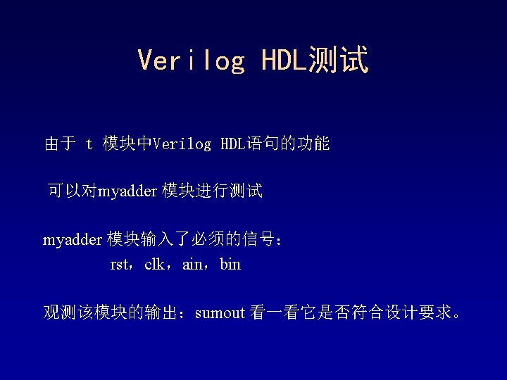
Verilog HDL模块的测试 `include myadder. v module t; wire [8: 0] sumout; reg [7: 0] ain, bin; reg clk; myadder(. clock(clk), . reset(rst), . a(ain), . b(bin), . sum(sumout)); initial begin rst = 1;clk = 0; ain = 0; bin=3; #70 rst=0; # 70 rst = 1;end always #50 clk = ~clk; always @(posedge clk) begin ain = ain + 2; bin = bin +5; endmodule
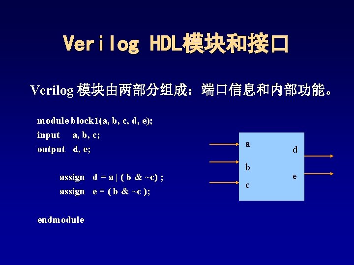
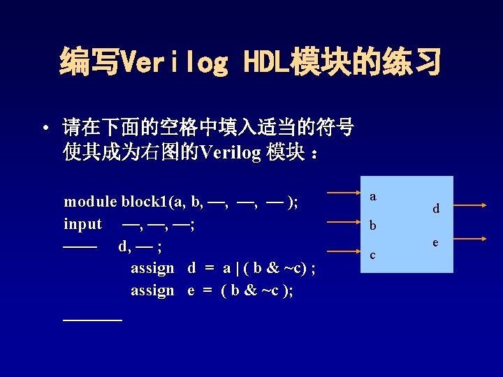
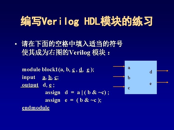
Verilog HDL模块和接口 Verilog 模块由两部分组成:端口信息和内部功能。 module block 1(a, b, c, d, e); input a, b, c; output d, e; assign d = a | ( b & ~c) ; assign e = ( b & ~c ); endmodule a b c d e
编写Verilog HDL模块的练习 • 请在下面的空格中填入适当的符号 使其成为右图的Verilog 模块 : module block 1(a, b, c , d, e ); input a, b, c; output d, e ; assign d = a | ( b & ~c) ; assign e = ( b & ~c ); endmodule a d b c e
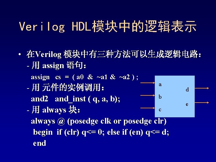
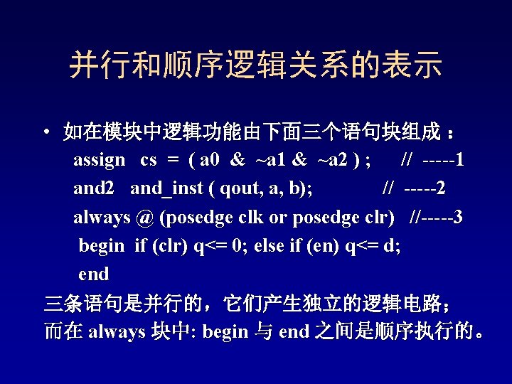
Verilog HDL模块中的逻辑表示 • 在Verilog 模块中有三种方法可以生成逻辑电路: - 用 assign 语句: assign cs = ( a 0 & ~a 1 & ~a 2 ) ; a - 用 元件的实例调用: b and 2 and_inst ( q, a, b); c - 用 always 块: always @ (posedge clk or posedge clr) begin if (clr) q<= 0; else if (en) q<= d; end d e
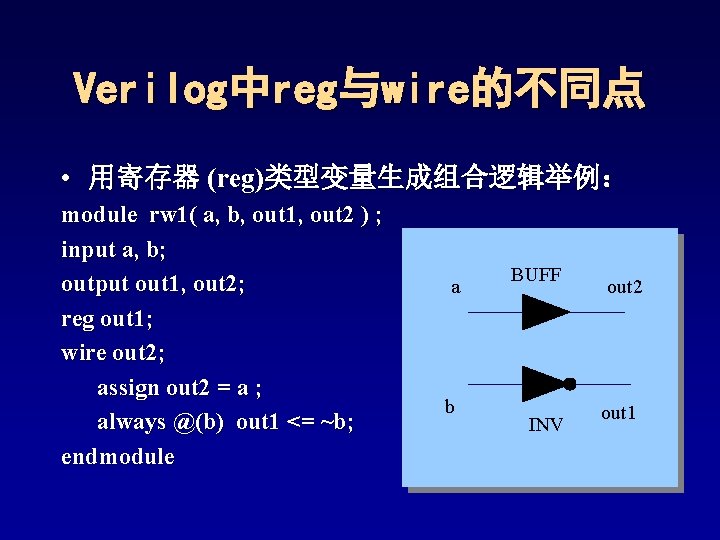
Verilog中reg与wire的不同点 • 用寄存器 (reg)类型变量生成组合逻辑举例: module rw 1( a, b, out 1, out 2 ) ; input a, b; output out 1, out 2; reg out 1; wire out 2; assign out 2 = a ; always @(b) out 1 <= ~b; endmodule a b BUFF INV out 2 out 1
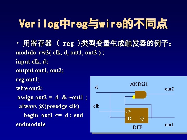
Verilog中reg与wire的不同点 • 用寄存器 ( reg )类型变量生成触发器的例子: module rw 2( clk, d, out 1, out 2 ) ; input clk, d; output out 1, out 2; reg out 1; d wire out 2; assign out 2 = d & ~out 1 ; clk always @(posedge clk) begin out 1 <= d ; endmodule AND 2 i 1 D out 2 Q DFF out 1
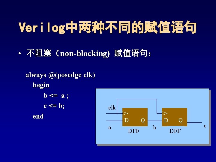
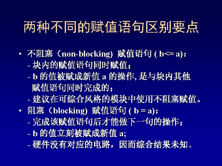
Verilog中两种不同的赋值语句 • 不阻塞(non-blocking) 赋值语句: always @(posedge clk) begin b <= a ; c <= b; end clk D a DFF Q D b Q DFF c
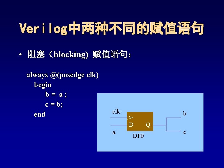
Verilog中两种不同的赋值语句 • 阻塞(blocking) 赋值语句: always @(posedge clk) begin b= a; c = b; end clk b D a DFF Q c
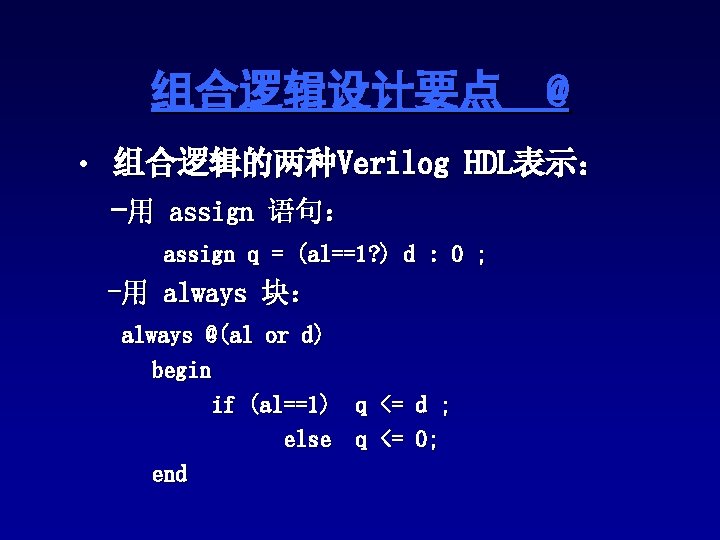
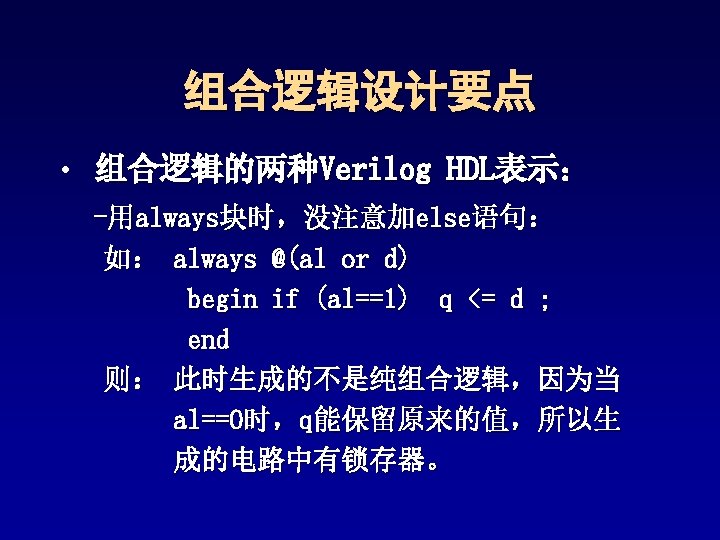
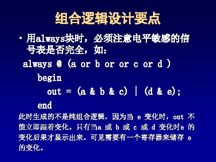
组合逻辑设计要点 @ • 组合逻辑的两种Verilog HDL表示: -用 assign 语句: assign q = (al==1? ) d : 0 ; -用 always 块: always @(al or d) begin if (al==1) q <= d ; else q <= 0; end
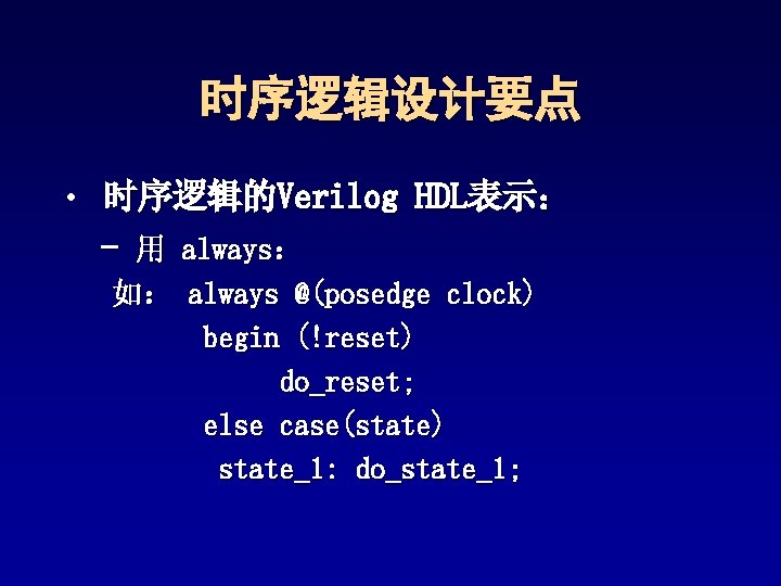
时序逻辑设计要点 • 时序逻辑的Verilog HDL表示: - 用 always: 如: always @(posedge clock) begin (!reset) do_reset; else case(state) state_1: do_state_1;
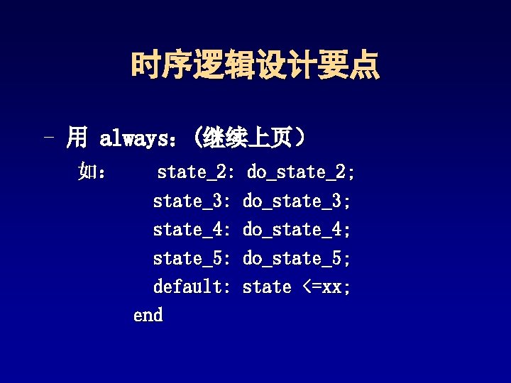
时序逻辑设计要点 - 用 always:(继续上页) 如: state_2: do_state_2; state_3: do_state_3; state_4: do_state_4; state_5: do_state_5; default: state <=xx; end
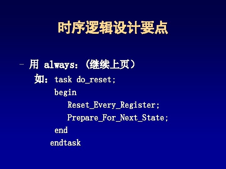
时序逻辑设计要点 - 用 always:(继续上页) 如:task do_reset; begin Reset_Every_Register; Prepare_For_Next_State; endtask
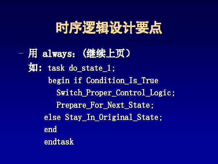
时序逻辑设计要点 - 用 always:(继续上页) 如: task do_state_1; begin if Condition_Is_True Switch_Proper_Control_Logic; Prepare_For_Next_State; else Stay_In_Original_State; endtask
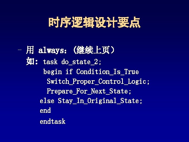
时序逻辑设计要点 - 用 always:(继续上页) 如: task do_state_2; begin if Condition_Is_True Switch_Proper_Control_Logic; Prepare_For_Next_State; else Stay_In_Original_State; endtask
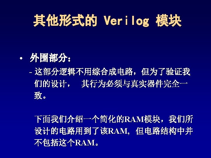
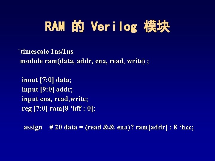
RAM 的 Verilog 模块 `timescale 1 ns/1 ns module ram(data, addr, ena, read, write) ; inout [7: 0] data; input [9: 0] addr; input ena, read, write; reg [7: 0] ram[8 ‘hff : 0]; assign # 20 data = (read && ena)? ram[addr] : 8 ‘hzz;
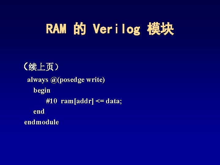
RAM 的 Verilog 模块 (续上页) always @(posedge write) begin #10 ram[addr] <= data; endmodule
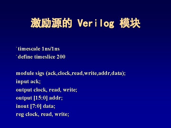
激励源的 Verilog 模块 `timescale 1 ns/1 ns `define timeslice 200 module sigs (ack, clock, read, write, addr, data); input ack; output clock, read, write; output [15: 0] addr; inout [7: 0] data; reg clock, read, write;
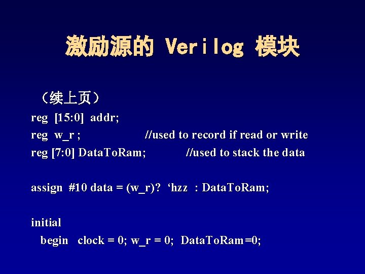
激励源的 Verilog 模块 (续上页) reg [15: 0] addr; reg w_r ; //used to record if read or write reg [7: 0] Data. To. Ram; //used to stack the data assign #10 data = (w_r)? ‘hzz : Data. To. Ram; initial begin clock = 0; w_r = 0; Data. To. Ram=0;
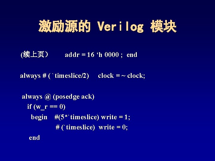
激励源的 Verilog 模块 (续上页) addr = 16 ‘h 0000 ; end always # ( `timeslice/2) clock = ~ clock; always @ (posedge ack) if (w_r == 0) begin #(5*`timeslice) write = 1; # (`timeslice) write = 0; end
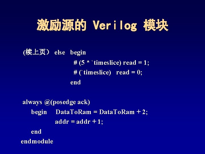
激励源的 Verilog 模块 (续上页) else begin # (5 * `timeslice) read = 1; # (`timeslice) read = 0; end always @(posedge ack) begin Data. To. Ram = Data. To. Ram + 2; addr = addr + 1; endmodule
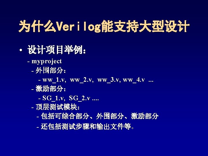
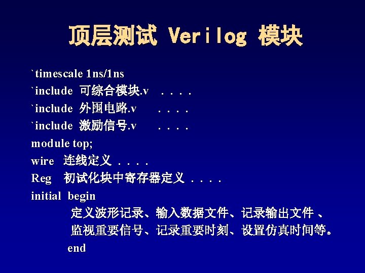
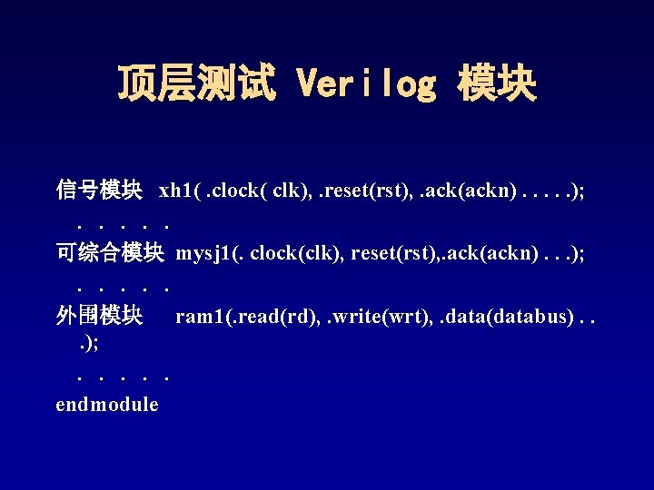
顶层测试 Verilog 模块 信号模块 xh 1(. clock( clk), . reset(rst), . ack(ackn). . . ); . . . 可综合模块 mysj 1(. clock(clk), reset(rst), . ack(ackn). . . ); . . . 外围模块 ram 1(. read(rd), . write(wrt), . data(databus). . . ); . . . endmodule
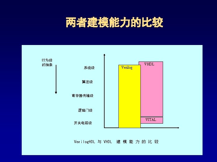
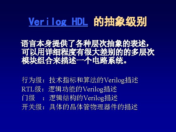
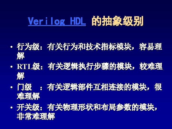
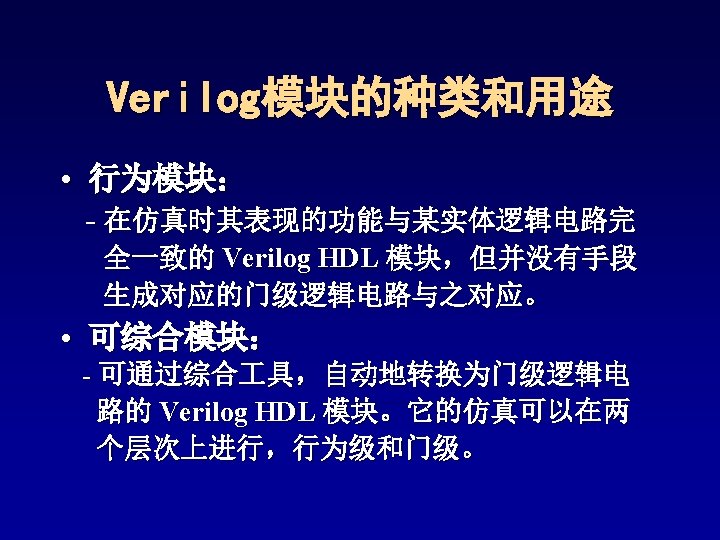
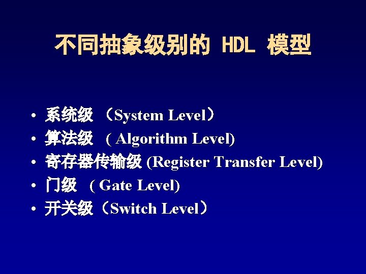
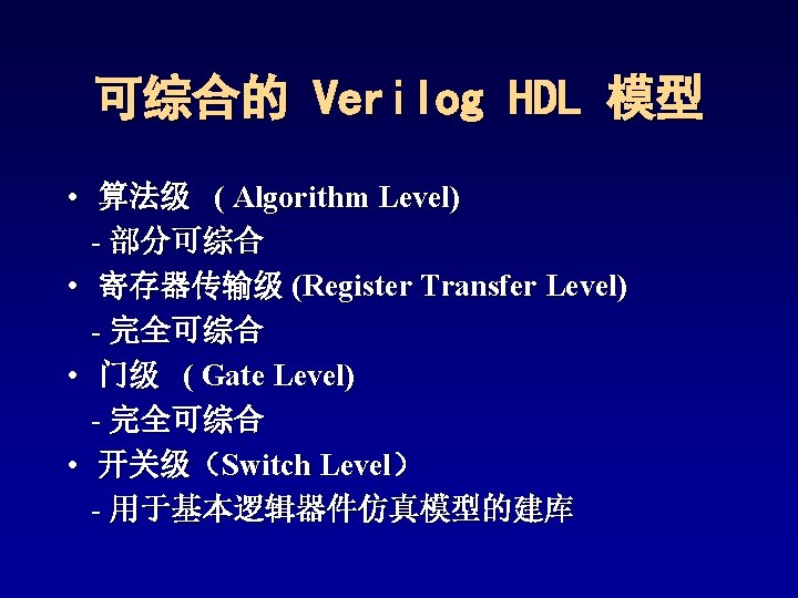
不同抽象级别的 HDL 模型 • • • 系统级 (System Level) 算法级 ( Algorithm Level) 寄存器传输级 (Register Transfer Level) 门级 ( Gate Level) 开关级(Switch Level)
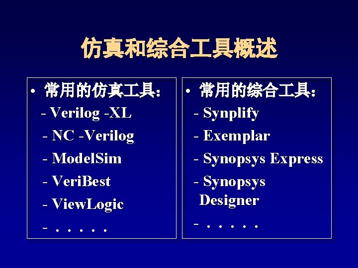
仿真和综合 具概述 • 常用的仿真 具: • 常用的综合 具: - Verilog -XL - Synplify - NC -Verilog - Exemplar - Model. Sim - Synopsys Express - Veri. Best - Synopsys Designer - View. Logic -. .