The Verilog Hardware Description Language GUIDELINES n How








![ROM description (1/2) module rominfr (data, en, addr); output [3: 0] data; input en; ROM description (1/2) module rominfr (data, en, addr); output [3: 0] data; input en;](https://slidetodoc.com/presentation_image_h/30ce6c151d2b09abd376a4053568eae2/image-49.jpg)
![ROM description (2/2) initial begin ROM[0] = 4’b 0001; ROM[1] = ROM[2] = 4’b ROM description (2/2) initial begin ROM[0] = 4’b 0001; ROM[1] = ROM[2] = 4’b](https://slidetodoc.com/presentation_image_h/30ce6c151d2b09abd376a4053568eae2/image-50.jpg)
![DUAL –PORT RAM (2/2) always @(posedge clk 1) begin if (we) ram[add 1] <= DUAL –PORT RAM (2/2) always @(posedge clk 1) begin if (we) ram[add 1] <=](https://slidetodoc.com/presentation_image_h/30ce6c151d2b09abd376a4053568eae2/image-52.jpg)
![Include files `include "timing. vh" module counter 1(count, reset, clk) ; output [7: 0] Include files `include "timing. vh" module counter 1(count, reset, clk) ; output [7: 0]](https://slidetodoc.com/presentation_image_h/30ce6c151d2b09abd376a4053568eae2/image-53.jpg)
![Parametric models `include “rominfr_pkg. vh” module rominfr (data, en, addr); output [`wordlength-1: 0] data; Parametric models `include “rominfr_pkg. vh” module rominfr (data, en, addr); output [`wordlength-1: 0] data;](https://slidetodoc.com/presentation_image_h/30ce6c151d2b09abd376a4053568eae2/image-54.jpg)

- Slides: 64

The Verilog Hardware Description Language

GUIDELINES n How to write HDL code:

GUIDELINES n How NOT to write HDL code:

Think Hardware NOT Software n Poorly written HDL code will either be: – Unsynthesizable – Functionally incorrect – Lead to poor performance/area/power results

Conventions n Verilog IS case sensitive – CLOCK, clock and Clock are different n Syntax is based on C – but is interpreted differently

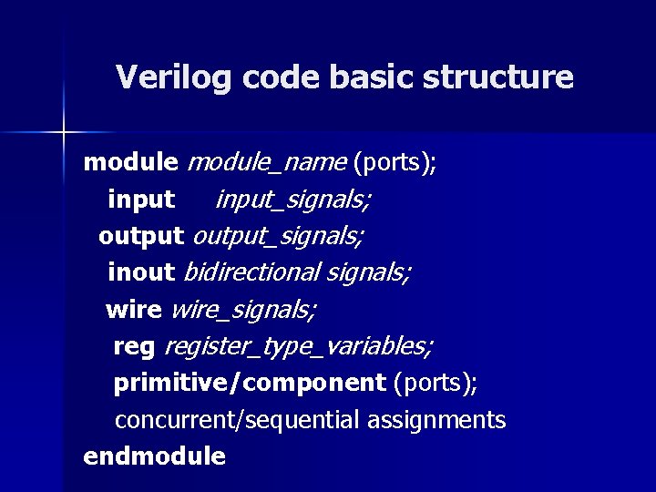
Verilog code basic structure module_name (ports); input_signals; output_signals; inout bidirectional signals; wire_signals; register_type_variables; primitive/component (ports); concurrent/sequential assignments endmodule

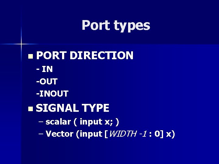
Port types n PORT DIRECTION - IN -OUT -INOUT n SIGNAL TYPE – scalar ( input x; ) – Vector (input [WIDTH -1 : 0] x)

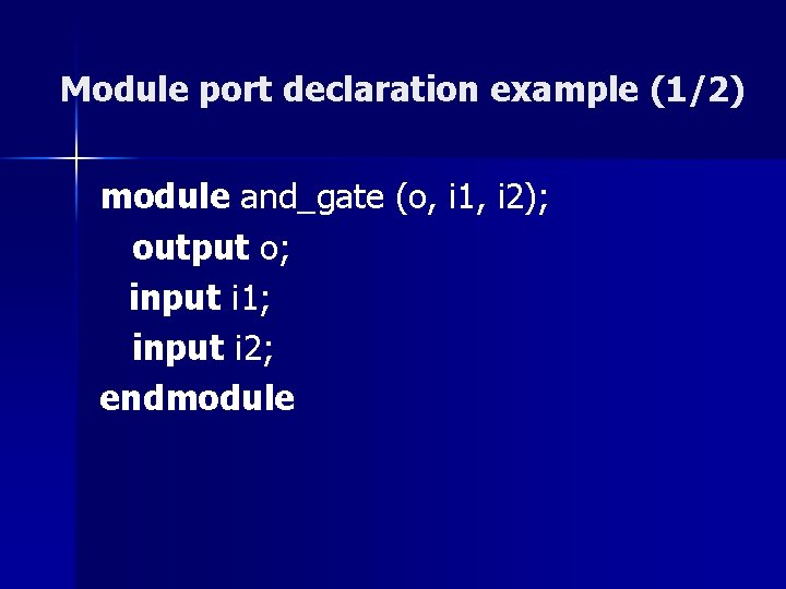
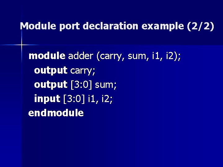
Module port declaration example (1/2) module and_gate (o, i 1, i 2); output o; input i 1; input i 2; endmodule

Module port declaration example (2/2) module adder (carry, sum, i 1, i 2); output carry; output [3: 0] sum; input [3: 0] i 1, i 2; endmodule

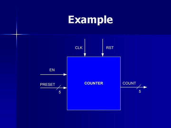
Example

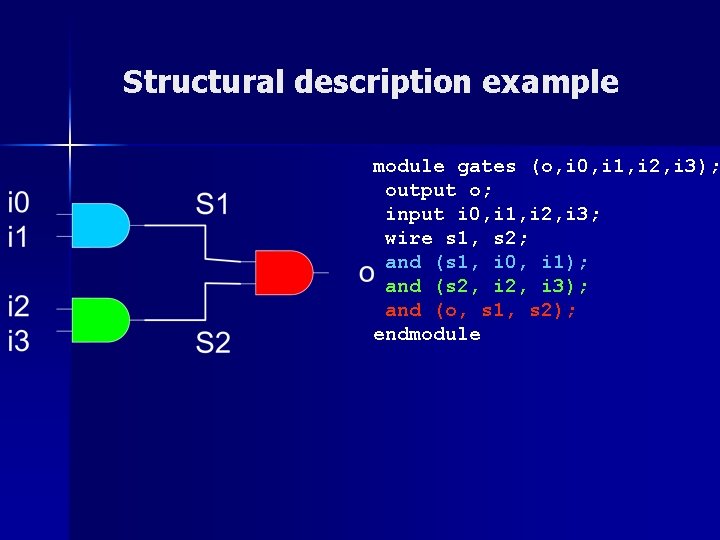
Verilog Primitives Verilog primitives are models of common combinational logic gates n Their functionality is built into the language and can be instantiated in designs directly n The output port of a primitive must be first in the list of ports n

Structural description example module gates (o, i 0, i 1, i 2, i 3); output o; input i 0, i 1, i 2, i 3; wire s 1, s 2; and (s 1, i 0, i 1); and (s 2, i 3); and (o, s 1, s 2); endmodule

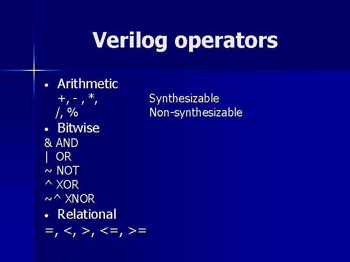
Verilog operators • Arithmetic +, - , *, /, % • Bitwise & AND | OR ~ NOT ^ XOR ~^ XNOR Relational =, <, >, <=, >= • Synthesizable Non-synthesizable

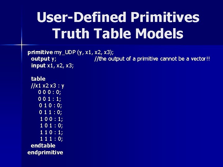
User-Defined Primitives Truth Table Models primitive my_UDP (y, x 1, x 2, x 3); output y; //the output of a primitive cannot be a vector!! input x 1, x 2, x 3; table //x 1 x 2 x 3 : y 0 0 0 : 0; 0 0 1 : 1; 0 1 0 : 0; 0 1 1 : 0; 1 0 0 : 1; 1 0 1 : 0; 1 1 0 : 1; 1 1 1 : 0; endtable endprimitive

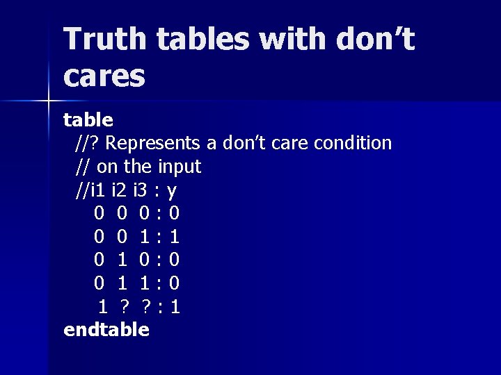
Truth tables with don’t cares table //? Represents a don’t care condition // on the input //i 1 i 2 i 3 : y 0 0 0: 0 0 0 1: 1 0: 0 0 1 1: 0 1 ? ? : 1 endtable

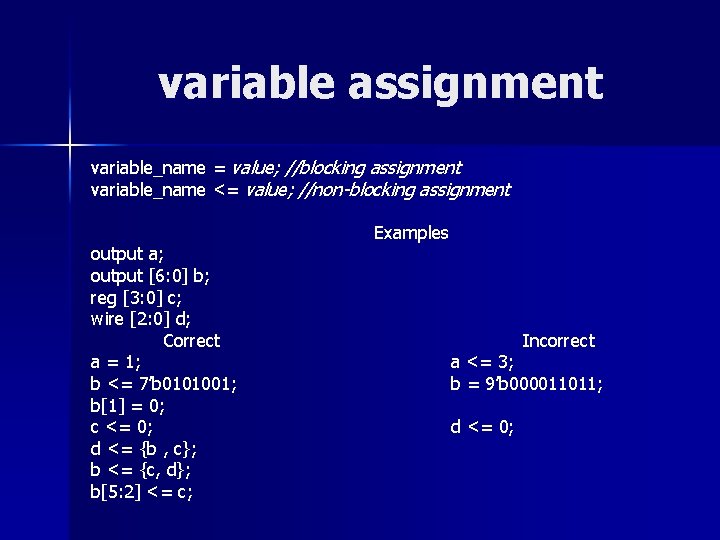
variable assignment variable_name = value; //blocking assignment variable_name <= value; //non-blocking assignment output a; output [6: 0] b; reg [3: 0] c; wire [2: 0] d; Correct a = 1; b <= 7’b 0101001; b[1] = 0; c <= 0; d <= {b , c}; b <= {c, d}; b[5: 2] <= c; Examples Incorrect a <= 3; b = 9’b 000011011; d <= 0;

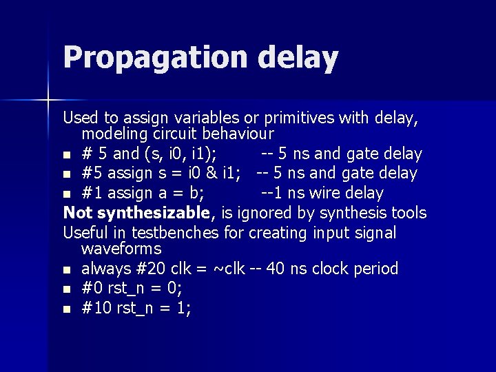
Propagation delay Used to assign variables or primitives with delay, modeling circuit behaviour n # 5 and (s, i 0, i 1); -- 5 ns and gate delay n #5 assign s = i 0 & i 1; -- 5 ns and gate delay n #1 assign a = b; --1 ns wire delay Not synthesizable, is ignored by synthesis tools Useful in testbenches for creating input signal waveforms n always #20 clk = ~clk -- 40 ns clock period n #0 rst_n = 0; n #10 rst_n = 1;

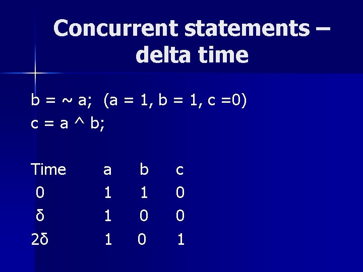
Concurrent statements – delta time b = ~ a; (a = 1, b = 1, c =0) c = a ^ b; Time 0 δ 2δ a 1 1 1 b 1 0 0 c 0 0 1

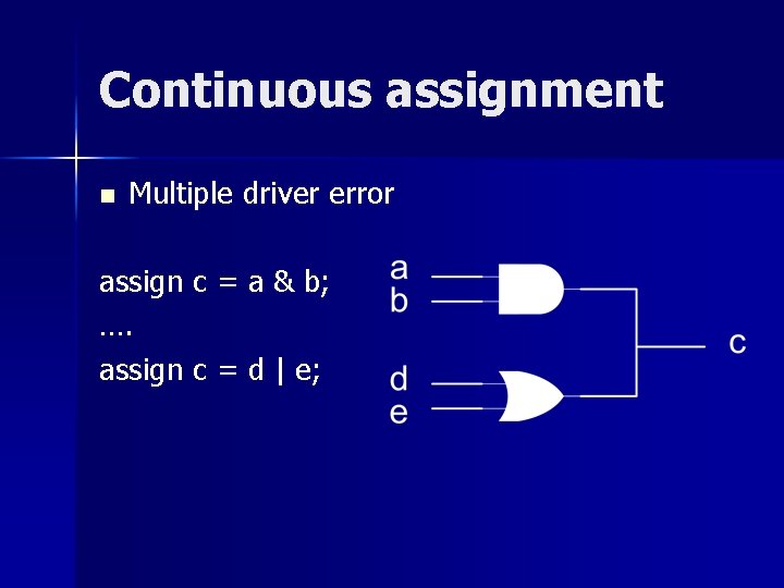
Continuous assignment n Multiple driver error assign c = a & b; …. assign c = d | e;

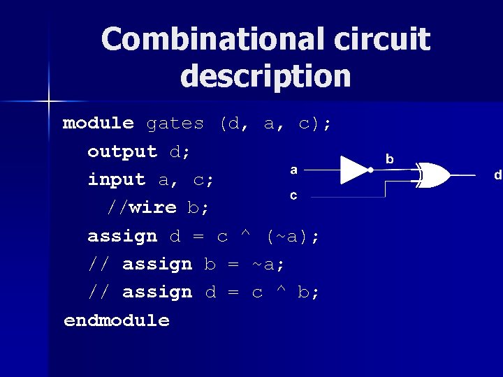
Combinational circuit description module gates (d, a, c); output d; input a, c; //wire b; assign d = c ^ (~a); // assign b = ~a; // assign d = c ^ b; endmodule

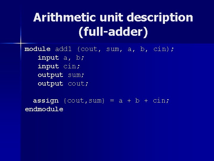
Arithmetic unit description (full-adder) module add 1 (cout, sum, a, b, cin); input a, b; input cin; output sum; output cout; assign {cout, sum} = a + b + cin; endmodule

Example Describe a 5 -bit multiplier in Verilog.

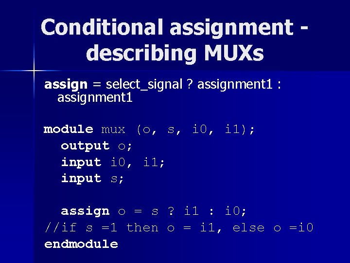
Conditional assignment describing MUXs assign = select_signal ? assignment 1 : assignment 1 module mux (o, s, i 0, i 1); output o; input i 0, i 1; input s; assign o = s ? i 1 : i 0; //if s =1 then o = i 1, else o =i 0 endmodule

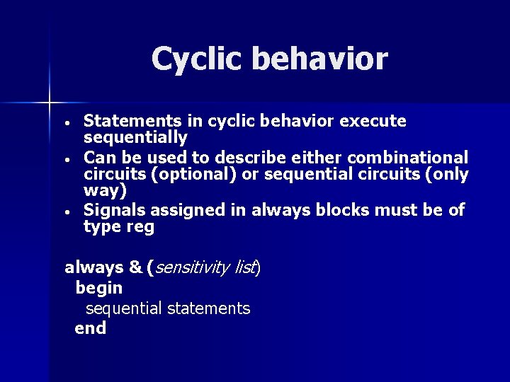
Cyclic behavior • • • Statements in cyclic behavior execute sequentially Can be used to describe either combinational circuits (optional) or sequential circuits (only way) Signals assigned in always blocks must be of type reg always & (sensitivity list) begin sequential statements end

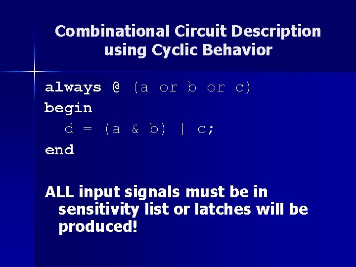
Combinational Circuit Description using Cyclic Behavior always @ (a or b or c) begin d = (a & b) | c; end ALL input signals must be in sensitivity list or latches will be produced!

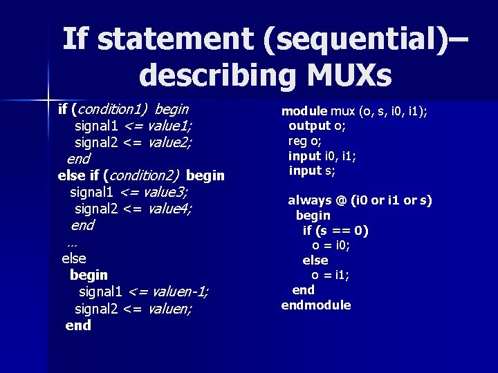
If statement (sequential)– describing MUXs if (condition 1) begin signal 1 <= value 1; signal 2 <= value 2; end else if (condition 2) begin signal 1 <= value 3; signal 2 <= value 4; end … else begin signal 1 <= valuen-1; signal 2 <= valuen; end module mux (o, s, i 0, i 1); output o; reg o; input i 0, i 1; input s; always @ (i 0 or i 1 or s) begin if (s == 0) o = i 0; else o = i 1; endmodule

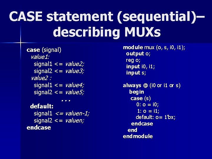
CASE statement (sequential)– describing MUXs case (signal) value 1: signal 1 <= value 2; signal 2 <= value 3; value 2 : signal 1 <= value 4; signal 2 <= value 5; . . . default: signal 1 <= valuen-1; signal 2 <= valuen; endcase module mux (o, s, i 0, i 1); output o; reg o; input i 0, i 1; input s; always @ (i 0 or i 1 or s) begin case (s) 0: o = i 0; 1: o = i 1; default: o= 1’bx; endcase endmodule

Example n Describe a 3 -bit 4 -to-1 MUX

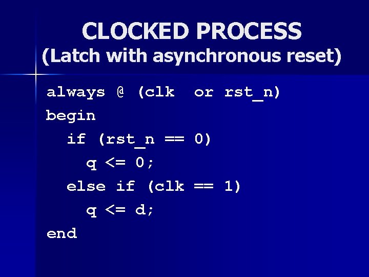
CLOCKED PROCESS (Latch with asynchronous reset) always @ (clk begin if (rst_n == q <= 0; else if (clk q <= d; end or rst_n) 0) == 1)

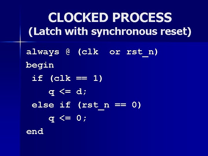
CLOCKED PROCESS (Latch with synchronous reset) always @ begin if (clk q <= else if q <= end (clk or rst_n) == 1) d; (rst_n == 0) 0;

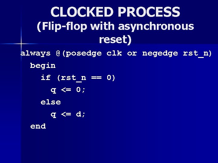
CLOCKED PROCESS (Flip-flop with asynchronous reset) always @(posedge clk or negedge rst_n) begin if (rst_n == 0) q <= 0; else q <= d; end

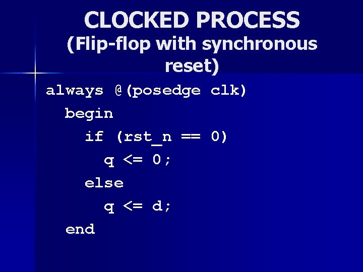
CLOCKED PROCESS (Flip-flop with synchronous reset) always @(posedge begin if (rst_n == q <= 0; else q <= d; end clk) 0)

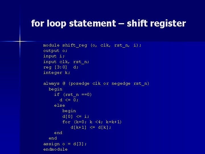
for loop statement – shift register module shift_reg (o, clk, rst_n, i); output o; input i; input clk, rst_n; reg [3: 0] d; integer k; always @ (posedge clk or negedge rst_n) begin if (rst_n ==0) d <= 0; else begin d[0] <= i; for (k=0; k <4; k=k+1) d[k+1] <= d[k]; end assign o = d[3]; endmodule

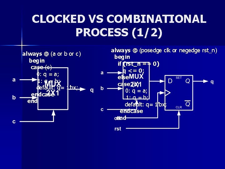
CLOCKED VS COMBINATIONAL PROCESS (1/2) always @ (a or b or c) begin case (c) 0: q = a; 1: q = b; default: q= 1’bx; endcase end always @ (posedge clk or negedge rst_n) begin if (rst_n == 0) q <= 0; else case (c) 0: q = a; 1: q = b; default: q= 1’bx; endcase end

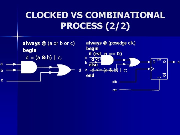
CLOCKED VS COMBINATIONAL PROCESS (2/2) always @ (a or b or c) begin d = (a & b) | c; end always @ (posedge clk) begin if (rst_n == 0) d <= 0; else d <= (a & b) | c; end

EXAMPLE n DESCIBE A BINARY UP/DOWN COUNTER WITH ENABLE THAT COUNTS UPTO 12 AND THEN STARTS AGAIN FROM ZERO

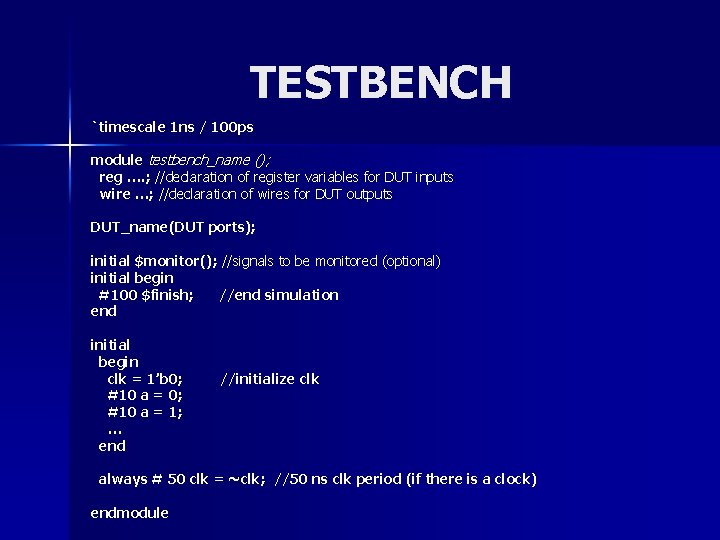
TESTBENCH `timescale 1 ns / 100 ps module testbench_name (); reg …. ; //declaration of register variables for DUT inputs wire …; //declaration of wires for DUT outputs DUT_name(DUT ports); initial $monitor(); //signals to be monitored (optional) initial begin #100 $finish; //end simulation end initial begin clk = 1’b 0; #10 a = 1; … end //initialize clk always # 50 clk = ~clk; //50 ns clk period (if there is a clock) endmodule

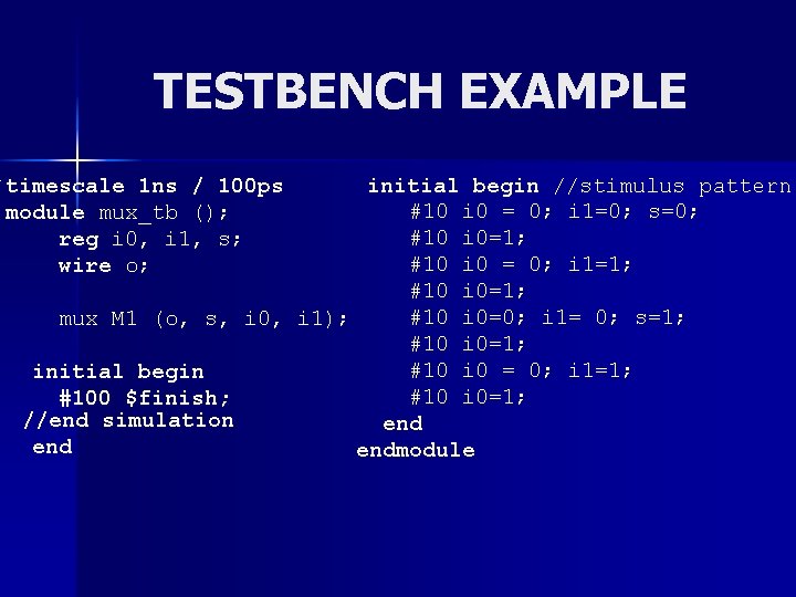
TESTBENCH EXAMPLE `timescale 1 ns / 100 ps module mux_tb (); reg i 0, i 1, s; wire o; initial begin //stimulus pattern #10 i 0 = 0; i 1=0; s=0; #10 i 0=1; #10 i 0 = 0; i 1=1; #10 i 0=0; i 1= 0; s=1; mux M 1 (o, s, i 0, i 1); #10 i 0=1; #10 i 0 = 0; i 1=1; initial begin #10 i 0=1; #100 $finish; //end simulation end endmodule

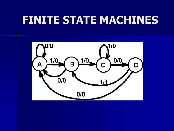
FINITE STATE MACHINES

FINITE STATE MACHINE IMPLEMENTATION

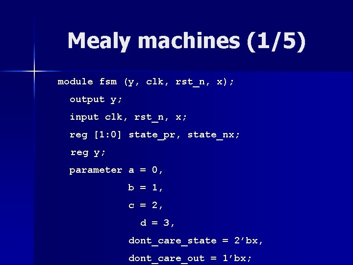
Mealy machines (1/5) module fsm (y, clk, rst_n, x); output y; input clk, rst_n, x; reg [1: 0] state_pr, state_nx; reg y; parameter a = 0, b = 1, c = 2, d = 3, dont_care_state = 2’bx, dont_care_out = 1’bx;

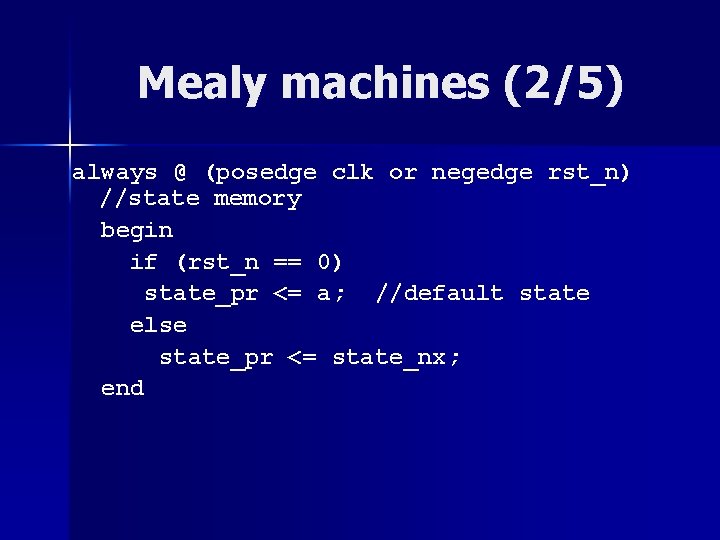
Mealy machines (2/5) always @ (posedge clk or negedge rst_n) //state memory begin if (rst_n == 0) state_pr <= a; //default state else state_pr <= state_nx; end

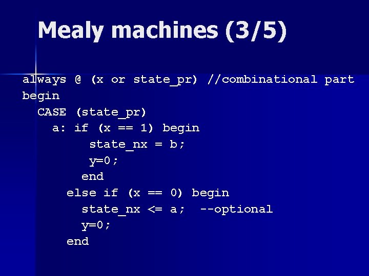
Mealy machines (3/5) always @ (x or state_pr) //combinational part begin CASE (state_pr) a: if (x == 1) begin state_nx = b; y=0; end else if (x == 0) begin state_nx <= a; --optional y=0; end

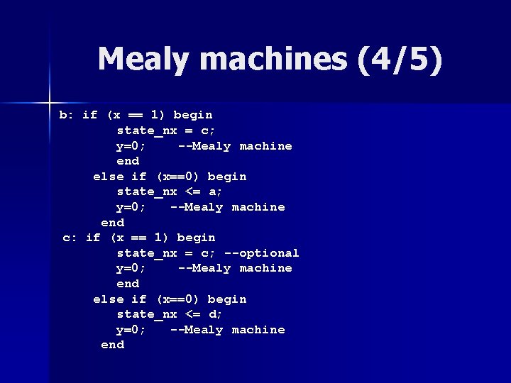
Mealy machines (4/5) b: if (x == 1) begin state_nx = c; y=0; --Mealy machine end else if (x==0) begin state_nx <= a; y=0; --Mealy machine end c: if (x == 1) begin state_nx = c; --optional y=0; --Mealy machine end else if (x==0) begin state_nx <= d; y=0; --Mealy machine end

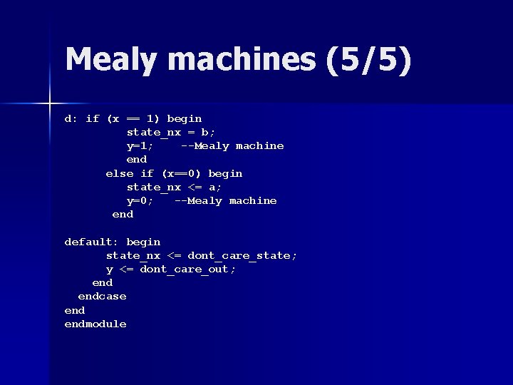
Mealy machines (5/5) d: if (x == 1) begin state_nx = b; y=1; --Mealy machine end else if (x==0) begin state_nx <= a; y=0; --Mealy machine end default: begin state_nx <= dont_care_state; y <= dont_care_out; endcase endmodule

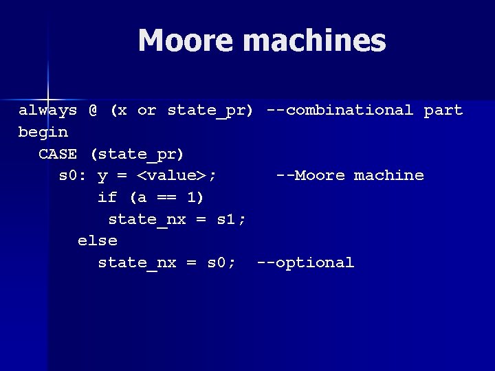
Moore machines always @ (x or state_pr) --combinational part begin CASE (state_pr) s 0: y = <value>; --Moore machine if (a == 1) state_nx = s 1; else state_nx = s 0; --optional

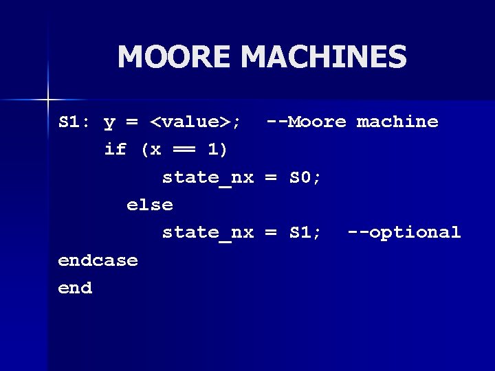
MOORE MACHINES S 1: y = <value>; --Moore machine if (x == 1) state_nx = S 0; else state_nx = S 1; --optional endcase end

EXAMPLE: OUT-OFSEQUENCE COUNTER n DESCRIBE A COUNTER WITH THE FOLLOWING SEQUENCE: – “ 000” => “ 011” => “ 001” => “ 111” => “ 000”
![ROM description 12 module rominfr data en addr output 3 0 data input en ROM description (1/2) module rominfr (data, en, addr); output [3: 0] data; input en;](https://slidetodoc.com/presentation_image_h/30ce6c151d2b09abd376a4053568eae2/image-49.jpg)
ROM description (1/2) module rominfr (data, en, addr); output [3: 0] data; input en; input [4: 0] addr; reg [3: 0] ROM [31: 0]; assign data = ROM[addr];
![ROM description 22 initial begin ROM0 4b 0001 ROM1 ROM2 4b ROM description (2/2) initial begin ROM[0] = 4’b 0001; ROM[1] = ROM[2] = 4’b](https://slidetodoc.com/presentation_image_h/30ce6c151d2b09abd376a4053568eae2/image-50.jpg)
ROM description (2/2) initial begin ROM[0] = 4’b 0001; ROM[1] = ROM[2] = 4’b 0011; ROM[3] = ROM[4] = 4’b 0101; ROM[5] = ROM[6] = 4’b 0111; ROM[7] = ROM[8] = 4’b 1001; ROM[9] = ROM[10] = 4’b 1011; ROM[11] ROM[12] = 4’b 1101; ROM[13] ROM[14] = 4’b 1111; ROM[15] ROM[16] = 4’b 0010; ROM[17] ROM[18] = 4’b 0100; ROM[19] ROM[20] = 4’b 0110; ROM[21] ROM[22] = 4’b 1000; ROM[23] ROM[24] = 4’b 1010; ROM[25] ROM[26] = 4’b 1100; ROM[27] ROM[28] = 4’b 1110; ROM[29] ROM[30] = 4’b 0000; ROM[31] endmodule 4’b 0010; 4’b 0100; 4’b 0110; 4’b 1000; 4’b 1010; = 4’b 1100; = 4’b 1110; = 4’b 0001; = 4’b 0011; = 4’b 0101; = 4’b 0111; = 4’b 1001; = 4’b 1011; = 4’b 1101; = 4’b 1111; = 4’b 0001;

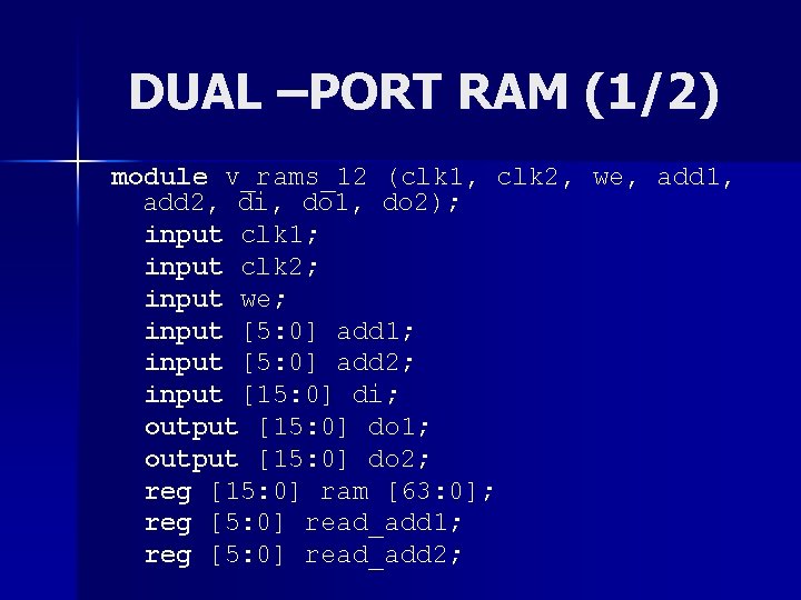
DUAL –PORT RAM (1/2) module v_rams_12 (clk 1, clk 2, we, add 1, add 2, di, do 1, do 2); input clk 1; input clk 2; input we; input [5: 0] add 1; input [5: 0] add 2; input [15: 0] di; output [15: 0] do 1; output [15: 0] do 2; reg [15: 0] ram [63: 0]; reg [5: 0] read_add 1; reg [5: 0] read_add 2;
![DUAL PORT RAM 22 always posedge clk 1 begin if we ramadd 1 DUAL –PORT RAM (2/2) always @(posedge clk 1) begin if (we) ram[add 1] <=](https://slidetodoc.com/presentation_image_h/30ce6c151d2b09abd376a4053568eae2/image-52.jpg)
DUAL –PORT RAM (2/2) always @(posedge clk 1) begin if (we) ram[add 1] <= di; read_add 1 <= add 1; end assign do 1 = ram[read_add 1]; always @(posedge clk 2) begin read_add 2 <= add 2; end assign do 2 = ram[read_add 2]; endmodule
![Include files include timing vh module counter 1count reset clk output 7 0 Include files `include "timing. vh" module counter 1(count, reset, clk) ; output [7: 0]](https://slidetodoc.com/presentation_image_h/30ce6c151d2b09abd376a4053568eae2/image-53.jpg)
Include files `include "timing. vh" module counter 1(count, reset, clk) ; output [7: 0] count; input reset, clk; reg [7: 0] count; always @(posedge clk or posedge reset) if(reset) count <= #(`REG_DELAY) 8'b 0; else count <= #(`REG_DELAY) count + 8 'b 1; . . . n //contents of ”timing. vh” file `timescale Ins/Ins `define REG_DELAY 1
![Parametric models include rominfrpkg vh module rominfr data en addr output wordlength1 0 data Parametric models `include “rominfr_pkg. vh” module rominfr (data, en, addr); output [`wordlength-1: 0] data;](https://slidetodoc.com/presentation_image_h/30ce6c151d2b09abd376a4053568eae2/image-54.jpg)
Parametric models `include “rominfr_pkg. vh” module rominfr (data, en, addr); output [`wordlength-1: 0] data; input en; input [`addr_size-1: 0] addr; reg [`wordlength-1: 0] ROM [`ROM_size-1: 0]; . . . //contents of “rominfr_pkg. vh” `define wordlength 8 `define addr_size 5 `define ROM_size 32

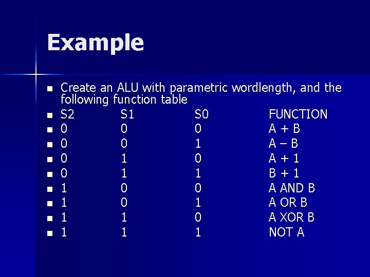
Example n n n n n Create an ALU with parametric wordlength, and the following function table S 2 S 1 S 0 FUNCTION 0 0 0 A+B 0 0 1 A–B 0 1 0 A+1 0 1 1 B+1 1 0 0 A AND B 1 0 1 A OR B 1 1 0 A XOR B 1 1 1 NOT A

Common Verilog Pitfalls

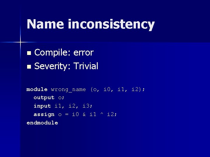
Name inconsistency Compile: error n Severity: Trivial n module wrong_name (o, i 0, i 1, i 2); output o; input i 1, i 2, i 3; assign o = i 0 & i 1 ^ i 2; endmodule

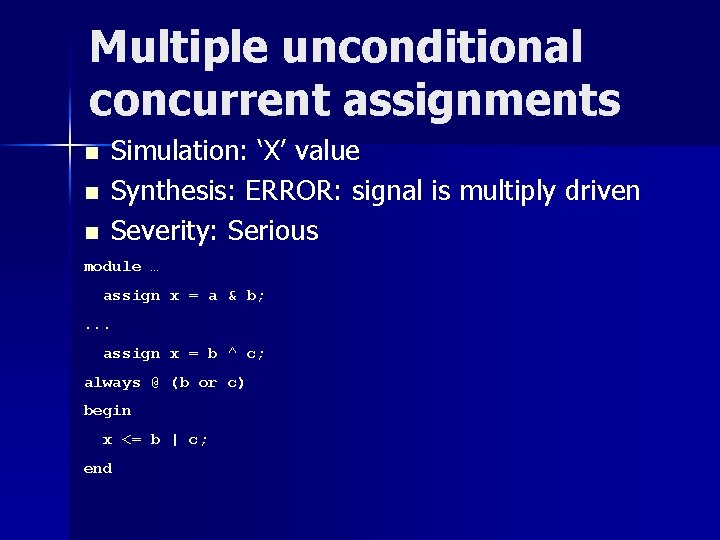
Multiple unconditional concurrent assignments n n n Simulation: ‘X’ value Synthesis: ERROR: signal is multiply driven Severity: Serious module … assign x = a & b; . . . assign x = b ^ c; always @ (b or c) begin x <= b | c; end

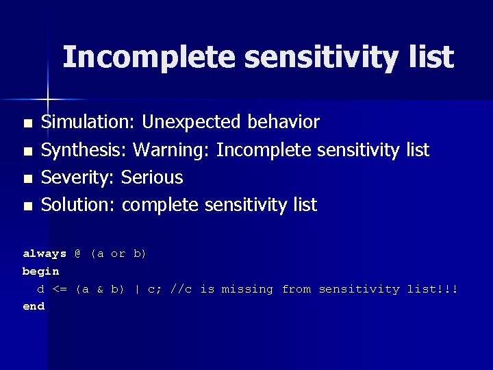
Incomplete sensitivity list n n Simulation: Unexpected behavior Synthesis: Warning: Incomplete sensitivity list Severity: Serious Solution: complete sensitivity list always @ (a or b) begin d <= (a & b) | c; //c is missing from sensitivity list!!! end

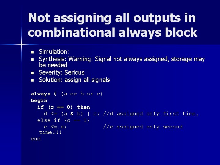
Not assigning all outputs in combinational always block n n Simulation: Synthesis: Warning: Signal not always assigned, storage may be needed Severity: Serious Solution: assign all signals always @ (a or b or c) begin if (c == 0) then d <= (a & b) | c; //d assigned only first time, else if (c == 1) e <= a; //e assigned only second time!!! end

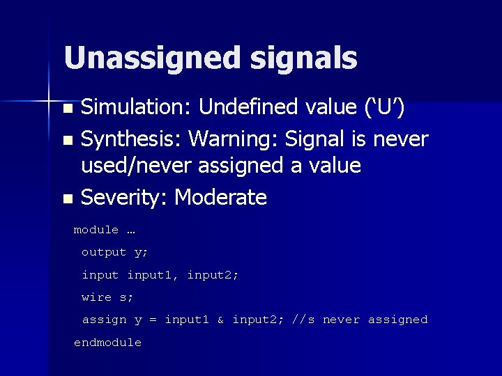
Unassigned signals Simulation: Undefined value (‘U’) n Synthesis: Warning: Signal is never used/never assigned a value n Severity: Moderate n module … output y; input 1, input 2; wire s; assign y = input 1 & input 2; //s never assigned endmodule

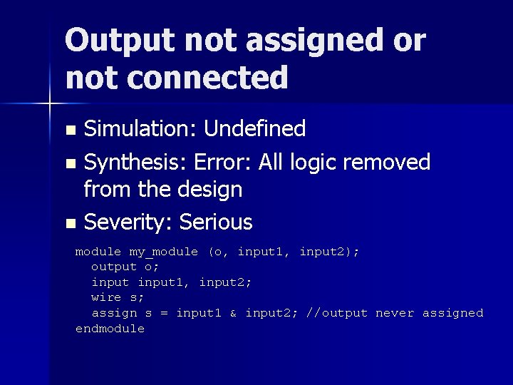
Output not assigned or not connected Simulation: Undefined n Synthesis: Error: All logic removed from the design n Severity: Serious n module my_module (o, input 1, input 2); output o; input 1, input 2; wire s; assign s = input 1 & input 2; //output never assigned endmodule

Using sequential instead of concurrent process Simulation: Unexpectedly delayed signals n Synthesis: More FFs than expected n

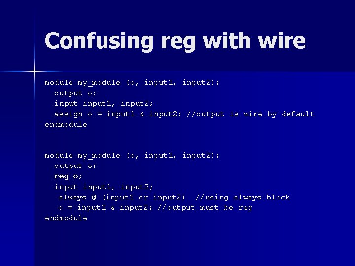
Confusing reg with wire module my_module (o, input 1, input 2); output o; input 1, input 2; assign o = input 1 & input 2; //output is wire by default endmodule my_module (o, input 1, input 2); output o; reg o; input 1, input 2; always @ (input 1 or input 2) //using always block o = input 1 & input 2; //output must be reg endmodule