Digital Design Chapter 5 RegisterTransfer Level RTL Design
- Slides: 88

Digital Design Chapter 5: Register-Transfer Level (RTL) Design Slides to accompany the textbook Digital Design, First Edition, by Frank Vahid, John Wiley and Sons Publishers, 2007. http: //www. ddvahid. com Copyright © 2007 Frank Vahid Instructors of courses requiring Vahid's Digital Design textbook (published by John Wiley and Sons) have permission to modify and use these slides for customary course-related activities, subject to keeping this copyright notice in place and unmodified. These slides may be posted as unanimated pdf versions on publicly-accessible course websites. . Power. Point source (or pdf Digital Design with animations) may not be posted to publicly-accessible websites, but may be posted for students on internal protected sites or distributed directly to students by other electronic means. Copyright © 2006 1 Instructors may make printouts of the slides available to students for a reasonable photocopying charge, without incurring royalties. Any other use requires explicit permission. Instructors Franksource Vahid may obtain Power. Point or obtain special use permissions from Wiley – see http: //www. ddvahid. com for information.

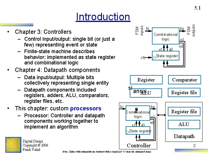
5. 1 • Chapter 3: Controllers – Control input/output: single bit (or just a few) representing event or state – Finite-state machine describes behavior; implemented as state register and combinational logic bi bo Combinational logic n 1 s 1 FSM outputs FSM inputs Introduction n 0 s 0 State register clk • Chapter 4: Datapath components – Data input/output: Multiple bits collectively representing single entity – Datapath components included registers, adders, ALU, comparators, register files, etc. • This chapter: custom processors – Processor: Controller and datapath components working together to implement an algorithm Digital Design Copyright © 2006 Frank Vahid Register si bi ansis ALU bo e z Combinational logic Comparator Register file n 1 n 0 s 1 s 0 State register Controller Note: Slides with animation are denoted with a small red "a" near the animated items ALU Datapath 2

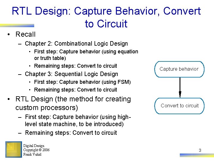
RTL Design: Capture Behavior, Convert to Circuit • Recall – Chapter 2: Combinational Logic Design • First step: Capture behavior (using equation or truth table) • Remaining steps: Convert to circuit – Chapter 3: Sequential Logic Design Capture behavior • First step: Capture behavior (using FSM) • Remaining steps: Convert to circuit • RTL Design (the method for creating custom processors) Convert to circuit – First step: Capture behavior (using highlevel state machine, to be introduced) – Remaining steps: Convert to circuit Digital Design Copyright © 2006 Frank Vahid 3

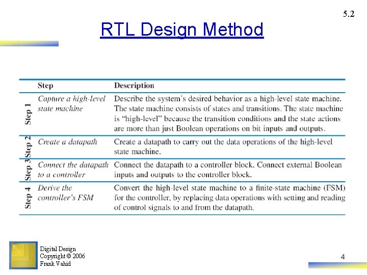
5. 2 RTL Design Method Digital Design Copyright © 2006 Frank Vahid 4

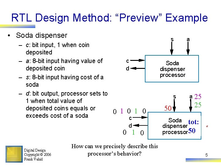
RTL Design Method: “Preview” Example • Soda dispenser – c: bit input, 1 when coin deposited c – a: 8 -bit input having value of deposited coin d – s: 8 -bit input having cost of a soda – d: bit output, processor sets to 1 when total value of deposited coins equals or 0 1 0 exceeds cost of a soda c d 0 1 0 Digital Design Copyright © 2006 Frank Vahid How can we precisely describe this processor’s behavior? s a Soda dispenser processor s 50 a 25 25 Soda tot: dispenser 25 processor 50 a 5

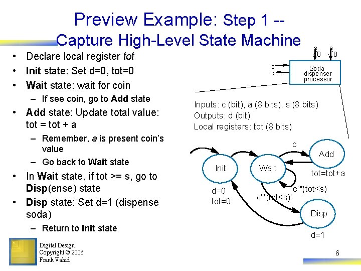
Preview Example: Step 1 -Capture High-Level State Machine • Declare local register tot • Init state: Set d=0, tot=0 • Wait state: wait for coin – If see coin, go to Add state • Add state: Update total value: tot = tot + a – Remember, a is present coin’s value – Go back to Wait state • In Wait state, if tot >= s, go to Disp(ense) state • Disp state: Set d=1 (dispense soda) – Return to Init state Digital Design Copyright © 2006 Frank Vahid c d s 8 a 8 Soda dispenser processor Inputs: c (bit), a (8 bits), s (8 bits) Outputs: d (bit) Local registers: tot (8 bits) c Add Init d=0 tot=0 Wait c’*(tot<s)’ tot=tot+a c’*(tot<s) Disp d=1 6

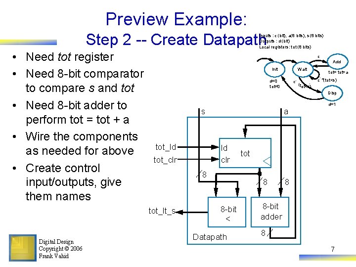
Preview Example: Step 2 -- Create Datapath Inputs : c (bit), a(8 bits), s (8 bits) Outputs : d (bit) Local reg isters: t ot (8 bits) • Need tot register • Need 8 -bit comparator to compare s and tot • Need 8 -bit adder to perform tot = tot + a • Wire the components as needed for above • Create control input/outputs, give them names c Add Init d=0 t ot=0 c‘ (t ot<s)‘ tot= t ot+a c‘ *(tot<s) Disp s tot_ld a ld clr tot_clr 8 tot_lt_s Digital Design Copyright © 2006 Frank Vahid Wait tot 8 8 -bit < Datapath d=1 8 8 -bit adder 8 7

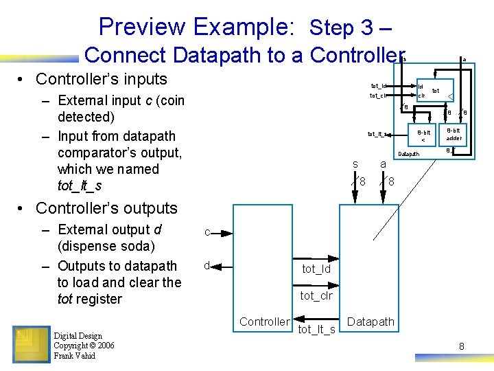
Preview Example: Step 3 – Connect Datapath to a Controller s • Controller’s inputs tot_ld ld clr tot_clr – External input c (coin detected) – Input from datapath comparator’s output, which we named tot_lt_s a 8 8 8 -bit < tot_lt_s Datapath s tot 8 8 -bit adder 8 a 8 8 • Controller’s outputs – External output d (dispense soda) – Outputs to datapath to load and clear the tot register c d tot_ld tot_clr Controller Digital Design Copyright © 2006 Frank Vahid tot_lt_s Datapath 8

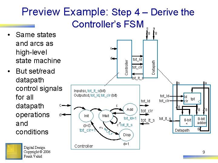
Preview Example: Step 4 – Derive the Controller’s FSM Digital Design Copyright © 2006 Frank Vahid d tot_ld tot_clr Datapath c Controller • Same states and arcs as high-level state machine • But set/read datapath control signals for all c datapath operations d and conditions s a 8 8 tot_lt_s s Inputs: : c, tot_lt_s (bit) Outputs: d, tot_ld, tot_clr (bit) tot_ld c Init d=0 tot_clr=1 Controller Wait c’* t ot_ lt_ s’ Add tot_ld=1 c’*tot_lt_s tot_ld tot_clr ld tpt clr 8 tot_clr tot_lt_s a tot_lt_s 8 8 -bit < Datapath 8 8 -bit adder 8 Disp d=1 9

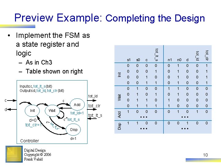
Preview Example: Completing the Design • Implement the FSM as a state register and logic – As in Ch 3 – Table shown on right Inputs: : c, tot_lt_s (bit) Outputs: d, tot_ld, tot_clr (bit) tot_ld c Init d=0 tot_clr=1 Wait c’* Digital Design Copyright © 2006 Frank Vahid tot_clr tot_ld=1 tot_lt_s c’*tot_lt_s tot Controller Add _lt _s ’ Disp d=1 10

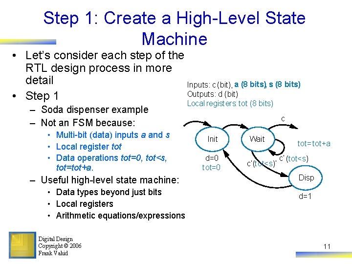
Step 1: Create a High-Level State Machine • Let’s consider each step of the RTL design process in more detail Inputs: c (bit), a (8 bits), s (8 bits) Outputs: d (bit) • Step 1 – Soda dispenser example – Not an FSM because: • Multi-bit (data) inputs a and s • Local register tot • Data operations tot=0, tot<s, tot=tot+a. – Useful high-level state machine: • Data types beyond just bits • Local registers • Arithmetic equations/expressions Digital Design Copyright © 2006 Frank Vahid Local registers: tot (8 bits) c Init d=0 tot=0 Wait c’(tot<s)’ tot= tot+a c’ (tot<s) Disp d=1 11

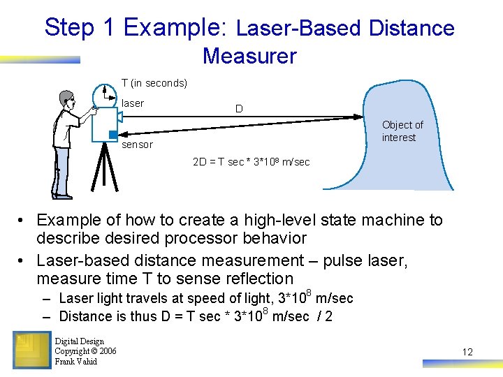
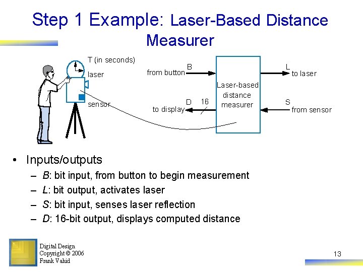
Step 1 Example: Laser-Based Distance Measurer T (in seconds) laser D Object of interest sensor 2 D = T sec * 3*108 m/sec • Example of how to create a high-level state machine to describe desired processor behavior • Laser-based distance measurement – pulse laser, measure time T to sense reflection – Laser light travels at speed of light, 3*108 m/sec – Distance is thus D = T sec * 3*108 m/sec / 2 Digital Design Copyright © 2006 Frank Vahid 12

Step 1 Example: Laser-Based Distance Measurer T (in seconds) laser sensor from button to display B D L 16 Laser-based distance measurer S to laser from sensor • Inputs/outputs – – B: bit input, from button to begin measurement L: bit output, activates laser S: bit input, senses laser reflection D: 16 -bit output, displays computed distance Digital Design Copyright © 2006 Frank Vahid 13

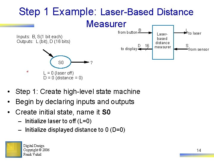
Step 1 Example: Laser-Based Distance Measurer from button B Inputs: B, S(1 bit each) Outputs: L (bit), D (16 bits) to display S 0 a D 16 Laserbased distance measurer L S to laser from sensor ? L = 0 (laser off) D = 0 (distance = 0) • Step 1: Create high-level state machine • Begin by declaring inputs and outputs • Create initial state, name it S 0 – Initialize laser to off (L=0) – Initialize displayed distance to 0 (D=0) Digital Design Copyright © 2006 Frank Vahid 14

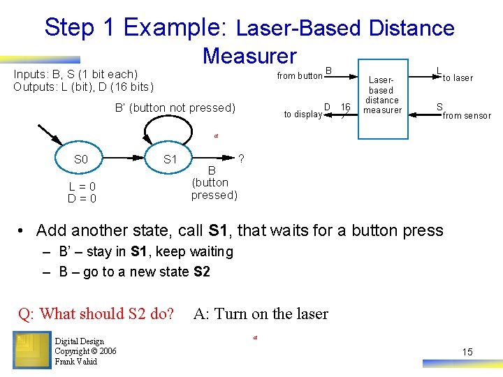
Step 1 Example: Laser-Based Distance Measurer from button B Inputs: B, S (1 bit each) Outputs: L (bit), D (16 bits) B’ (button not pressed) to display D 16 Laserbased distance measurer L S to laser from sensor a S 0 S 1 L=0 D=0 B (button pressed) ? • Add another state, call S 1, that waits for a button press – B’ – stay in S 1, keep waiting – B – go to a new state S 2 Q: What should S 2 do? Digital Design Copyright © 2006 Frank Vahid A: Turn on the laser a 15

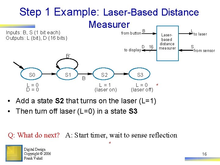
Step 1 Example: Laser-Based Distance Measurer from button B Inputs: B, S (1 bit each) Outputs: L (bit), D (16 bits) to display D Laserbased distance measurer 16 L S to laser from sensor B’ S 0 L=0 D=0 S 1 B S 2 S 3 L=1 (laser on) L=0 (laser off) a • Add a state S 2 that turns on the laser (L=1) • Then turn off laser (L=0) in a state S 3 Q: What do next? A: Start timer, wait to sense reflection a Digital Design Copyright © 2006 Frank Vahid 16

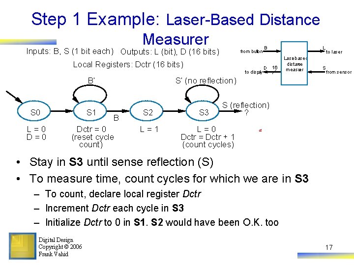
Step 1 Example: Laser-Based Distance Measurer Inputs: B, S (1 bit each) Outputs: L (bit), D (16 bits) from button Local Registers: Dctr (16 bits) to display B’ B D L 16 Lase r-based distance measu rer S to laser from sensor S’ (no reflection) S 0 S 1 L=0 Dctr = 0 (reset cycle count) B S 2 L=1 S 3 S (reflection) ? L=0 Dctr = Dctr + 1 (count cycles) a • Stay in S 3 until sense reflection (S) • To measure time, count cycles for which we are in S 3 – To count, declare local register Dctr – Increment Dctr each cycle in S 3 – Initialize Dctr to 0 in S 1. S 2 would have been O. K. too Digital Design Copyright © 2006 Frank Vahid 17

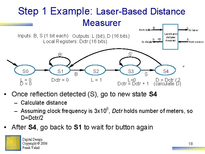
Step 1 Example: Laser-Based Distance Measurer from button Inputs: B, S (1 bit each) Outputs: L (bit), D (16 bits) Local Registers: Dctr (16 bits) to display B D L 16 Lase r-based distance measu rer S to laser from sensor S’ B’ a S 0 S 1 L=0 Dctr = 0 B S 2 L=1 S 3 S S 4 L=0 D = Dctr / 2 Dctr = Dctr + 1 (calculate D) • Once reflection detected (S), go to new state S 4 – Calculate distance – Assuming clock frequency is 3 x 10⁸, Dctr holds number of meters, so D=Dctr/2 • After S 4, go back to S 1 to wait for button again Digital Design Copyright © 2006 Frank Vahid 18

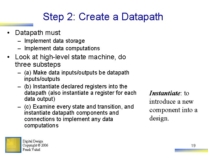
Step 2: Create a Datapath • Datapath must – Implement data storage – Implement data computations • Look at high-level state machine, do three substeps – (a) Make data inputs/outputs be datapath inputs/outputs – (b) Instantiate declared registers into the datapath (also instantiate a register for each data output) – (c) Examine every state and transition, and instantiate datapath components and connections to implement any data computations Digital Design Copyright © 2006 Frank Vahid Instantiate: to introduce a new component into a design. 19

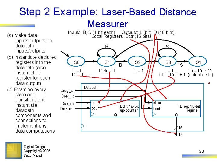
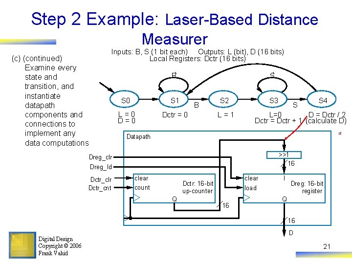
Step 2 Example: Laser-Based Distance Measurer Inputs: B, S (1 bit each) Outputs: L (bit), D (16 bits) (a) Make data Local Registers: Dctr (16 bits) inputs/outputs be datapath B‘ S‘ inputs/outputs (b) Instantiate declared S 4 S 0 S 1 S 2 S 3 registers into the B S datapath (also L=0 Dctr = 0 L=1 L=0 D = Dctr / 2 instantiate a D=0 Dctr = Dctr + 1 (calculate D) register for each a data output) Datapath (c) Examine every Dreg_clr state and Dreg_ld transition, and clear I Dctr_clr instantiate Dctr: 16 -bit Dreg: 16 -bit count Dctr_cnt load up-counter register datapath Q Q components and connections to implement any 16 data computations D Digital Design Copyright © 2006 Frank Vahid 20

Step 2 Example: Laser-Based Distance Measurer (c) (continued) Examine every state and transition, and instantiate datapath components and connections to implement any data computations Inputs: B, S (1 bit each) Outputs: L (bit), D (16 bits) Local Registers: Dctr (16 bits) B‘ S‘ S 0 S 1 L=0 Dctr = 0 B S 2 L=1 S 3 S S 4 L=0 D = Dctr / 2 Dctr = Dctr + 1 (calculate D) a Datapath >>1 16 Dreg_clr Dreg_ld Dctr_clr Dctr_cnt clear count clear Dctr: 16 -bit up-counter Q I load 16 Dreg: 16 -bit register Q 16 Digital Design Copyright © 2006 Frank Vahid D 21

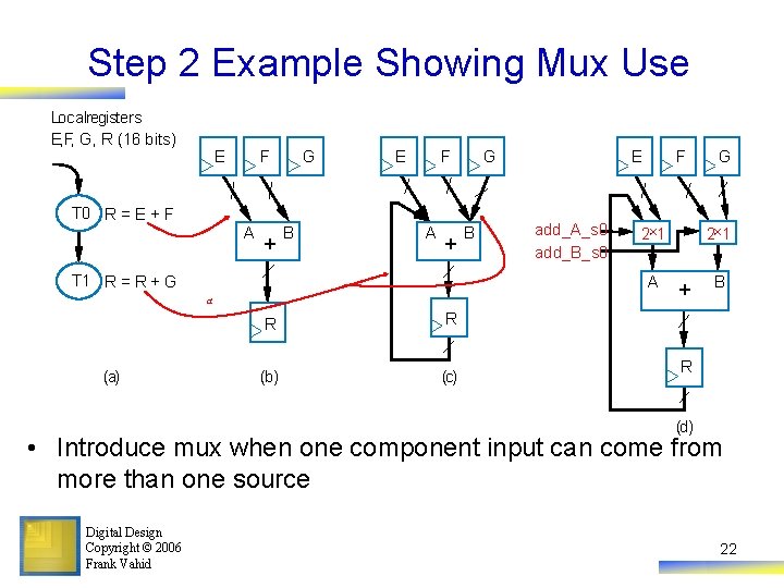
Step 2 Example Showing Mux Use Localregisters: E, F, G, R (16 bits) E T 0 R = E + F F A + G B E F A + T 1 R = R + G B E add_A_s 0 add_B_s 0 F × 1 2× A a (a) G R R (b) (c) G × 1 2× + B R (d) • Introduce mux when one component input can come from more than one source Digital Design Copyright © 2006 Frank Vahid 22

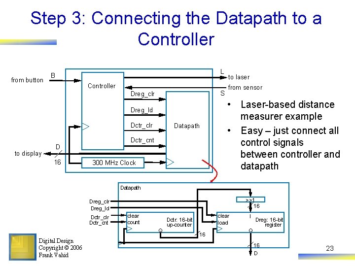
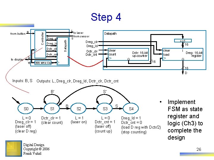
Step 3: Connecting the Datapath to a Controller from button L B Controller S Dreg_clr Dreg_ld Dctr_clr to display Dctr_cnt D 16 Datapath 300 MHz Clock to laser from sensor • Laser-based distance measurer example • Easy – just connect all control signals between controller and datapath Datapath >>1 16 Dreg_clr Dreg_ld Dctr_clr Dctr_cnt clear count Q Digital Design Copyright © 2006 Frank Vahid clear load Dctr: 16 -bit up-counter 16 I Q Dreg: 16 -bit register 16 D 23

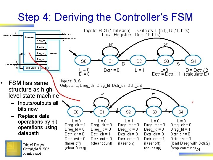
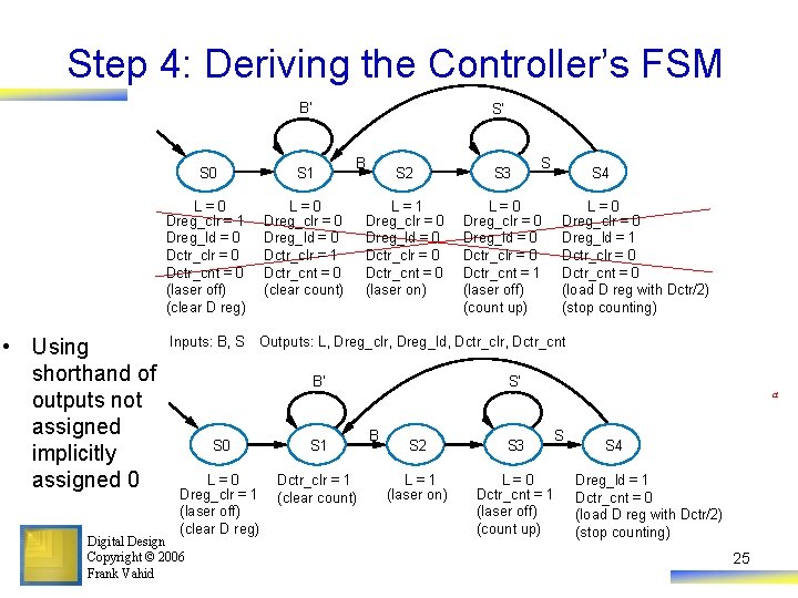
Step 4: Deriving the Controller’s FSM from butt on L B Controller to laser from sensor Inputs: B, S (1 bit each) Outputs: L (bit), D (16 bits) Local Registers: Dctr (16 bits) S Dreg_clr B’ Dreg_ld Dctr_clr Datapath Dctr_cnt D to display 16 S’ 300 MHz Clock S 0 S 1 L=0 Dctr = 0 S 2 B L=1 Inputs: B, S • FSM has same Outputs: L, Dreg_clr, Dreg_ld, Dctr_clr, Dctr_cnt structure as high. B’ level state machine – Inputs/outputs all bits now – Replace data operations by bit operations using datapath Digital Design Copyright © 2006 Frank Vahid S 3 S S 4 L=0 D = Dctr / 2 Dctr = Dctr + 1 (calculate D) S’ a S 0 S 1 L=0 Dreg_clr = 1 Dreg_ld = 0 Dctr_clr = 0 Dctr_cnt = 0 (laser off) (clear D reg) L=0 Dreg_clr = 0 Dreg_ld = 0 Dctr_clr = 1 Dctr_cnt = 0 (clear count) B S S 2 S 3 L=1 Dreg_clr = 0 Dreg_ld = 0 Dctr_clr = 0 Dctr_cnt = 0 (laser on) L=0 Dreg_clr = 0 Dreg_ld = 0 Dctr_clr = 0 Dctr_cnt = 1 (laser off) (count up) S 4 L=0 Dreg_clr = 0 Dreg_ld = 1 Dctr_clr = 0 Dctr_cnt = 0 (load D reg with Dctr/2) (stop counting)24

Step 4: Deriving the Controller’s FSM B’ • Using shorthand of outputs not assigned implicitly assigned 0 S’ S 0 S 1 L=0 Dreg_clr = 1 Dreg_ld = 0 Dctr_clr = 0 Dctr_cnt = 0 (laser off) (clear D reg) L=0 Dreg_clr = 0 Dreg_ld = 0 Dctr_clr = 1 Dctr_cnt = 0 (clear count) Inputs: B, S B S 3 L=1 Dreg_clr = 0 Dreg_ld = 0 Dctr_clr = 0 Dctr_cnt = 0 (laser on) L=0 Dreg_clr = 0 Dreg_ld = 0 Dctr_clr = 0 Dctr_cnt = 1 (laser off) (count up) S 4 L=0 Dreg_clr = 0 Dreg_ld = 1 Dctr_clr = 0 Dctr_cnt = 0 (load D reg with Dctr/2) (stop counting) Outputs: L, Dreg_clr, Dreg_ld, Dctr_clr, Dctr_cnt B’ S 0 S 1 L=0 Dreg_clr = 1 (laser off) (clear D reg) Dctr_clr = 1 (clear count) Digital Design Copyright © 2006 Frank Vahid S S 2 S’ B a S S 2 S 3 L=1 (laser on) L=0 Dctr_cnt = 1 (laser off) (count up) S 4 Dreg_ld = 1 Dctr_cnt = 0 (load D reg with Dctr/2) (stop counting) 25

Step 4 L Dreg_clr Dreg_ld Dctr_clr to display S to laser from sensor Datapath >>1 16 Dreg_clr Dreg_ld clear count Dctr_clr Dctr_cnt D 16 Datapath B Controller from button Q 300 MHz Clock clear load Dctr: 16 -bit up-counter 16 I Q Dreg: 16 -bit register 16 D Inputs: B, S Outputs: L, Dreg_clr, Dreg_ld, Dctr_clr, Dctr_cnt B’ S 0 S 1 L=0 Dreg_clr = 1 (laser off) (clear D reg) Dctr_clr = 1 (clear count) Digital Design Copyright © 2006 Frank Vahid S’ B S S 2 S 3 L=1 (laser on) L=0 Dctr_cnt = 1 (laser off) (count up) • Implement S 4 FSM as state register and Dreg_ld = 1 Dctr_cnt = 0 logic (Ch 3) to (load D reg with Dctr/2) complete the (stop counting) design 26

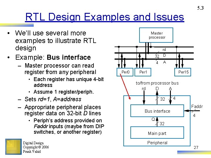
5. 3 RTL Design Examples and Issues • We’ll use several more examples to illustrate RTL design • Example: Bus interface – Master processor can read register from any peripheral • Each register has unique 4 -bit address • Assume 1 register/periph. – Sets rd=1, A=address – Appropriate peripheral places register data on 32 -bit D lines • Periph’s address provided on Faddr inputs (maybe from DIP switches, or another register) Digital Design Copyright © 2006 Frank Vahid Master processor rd 32 D 4 A Per 0 Per 15 to/from processor bus rd D A 32 Bus interface Q 4 Faddr 4 32 Main part Peripheral 27

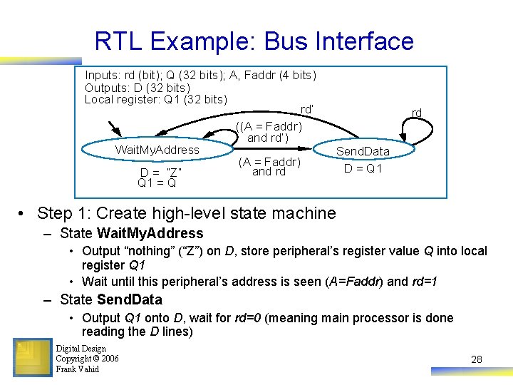
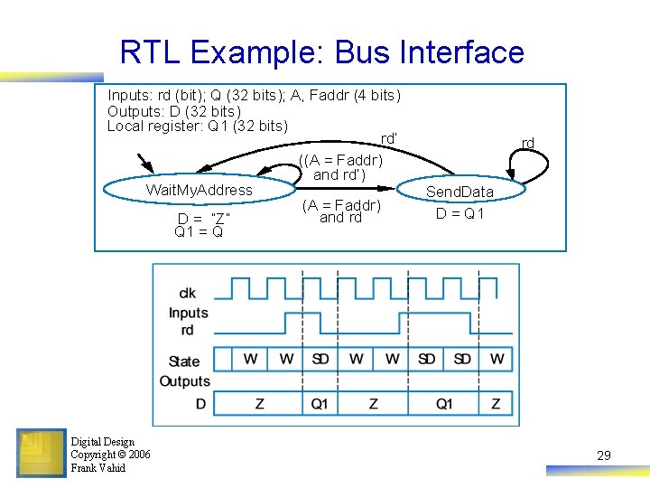
RTL Example: Bus Interface Inputs: rd (bit); Q (32 bits); A, Faddr (4 bits) Outputs: D (32 bits) Local register: Q 1 (32 bits) rd’ ((A = Faddr) and rd’) Wait. My. Address (A = Faddr) and rd D = “Z” Q 1 = Q rd Send. Data D = Q 1 • Step 1: Create high-level state machine – State Wait. My. Address • Output “nothing” (“Z”) on D, store peripheral’s register value Q into local register Q 1 • Wait until this peripheral’s address is seen (A=Faddr) and rd=1 – State Send. Data • Output Q 1 onto D, wait for rd=0 (meaning main processor is done reading the D lines) Digital Design Copyright © 2006 Frank Vahid 28

RTL Example: Bus Interface Inputs: rd (bit); Q (32 bits); A, Faddr (4 bits) Outputs: D (32 bits) Local register: Q 1 (32 bits) rd’ ((A = Faddr) and rd’) Wait. My. Address (A = Faddr) and rd D = “Z” Q 1 = Q Digital Design Copyright © 2006 Frank Vahid rd Send. Data D = Q 1 29

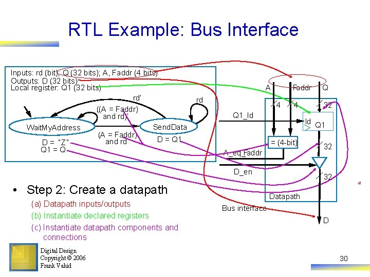
RTL Example: Bus Interface Inputs: rd (bit); Q (32 bits); A, Faddr (4 bits) Outputs: D (32 bits) Local register: Q 1 (32 bits) rd’ ((A = Faddr) and rd)’ Send. Data Wait. My. Address (A = Faddr) D = Q 1 and rd D = “Z” Q 1 = Q A rd 4 Faddr Q 4 32 Q 1_ld ld Q 1 = (4 -bit) A_eq_Faddr D_en • Step 2: Create a datapath (a) Datapath inputs/outputs (b) Instantiate declared registers (c) Instantiate datapath components and connections Digital Design Copyright © 2006 Frank Vahid 32 32 a Datapath Bus interface D 30

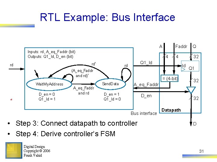
RTL Example: Bus Interface Inputs: rd (bit); Q (32 bits); A, Faddr (4 bits) Outputs: D (32 bits) Local register: Q 1 (32 bits) rd’ Inputs: rd, A_eq_Faddr ((A =(bit) Faddr) Outputs: Q 1_ld, D_enand (bit)rd)’ ‘ rd. Send. Data rd Wait. My. Address (A = Faddr) D = Q 1 and(A_eq_Faddr rd D = “Z” and rd)‘ Q 1 = Q Wait. My. Address a D_en = 0 Q 1_ld = 1 Send. Data A_eq_Faddr and rd A rd 4 Q 4 32 Q 1_ld rd ld = (4 -bit) A_eq_Faddr D_en = 1 Q 1_ld = 0 D_en Bus interface • Step 3: Connect datapath to controller • Step 4: Derive controller’s FSM Digital Design Copyright © 2006 Frank Vahid Faddr Q 1 32 32 Datapath D 31

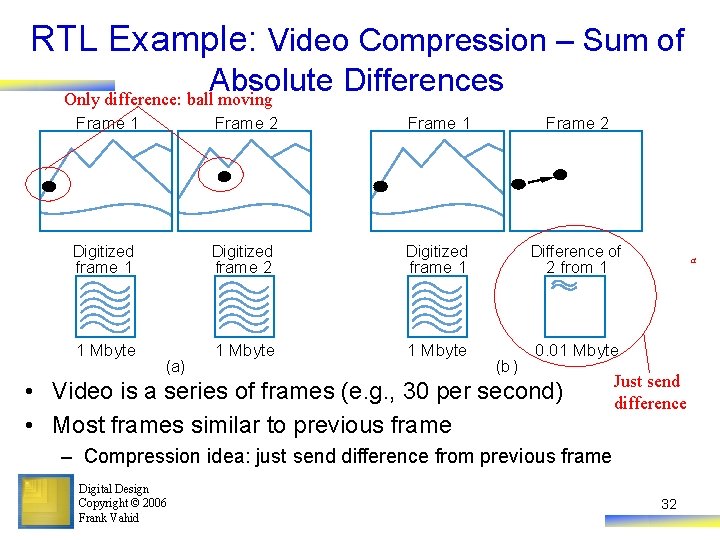
RTL Example: Video Compression – Sum of Absolute Differences Only difference: ball moving Frame 1 Frame 2 Digitized Difference of 1 Mbyte 0. 01 Mbyte frame 1 frame 2 (a) frame 1 a 2 from 1 (b) • Video is a series of frames (e. g. , 30 per second) • Most frames similar to previous frame Just send difference – Compression idea: just send difference from previous frame Digital Design Copyright © 2006 Frank Vahid 32

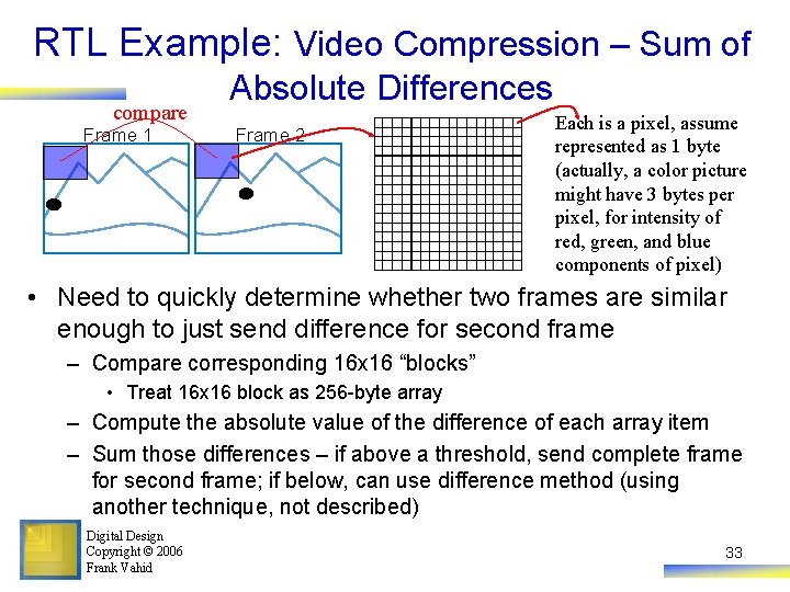
RTL Example: Video Compression – Sum of compare Frame 1 Absolute Differences Frame 2 Each is a pixel, assume represented as 1 byte (actually, a color picture might have 3 bytes per pixel, for intensity of red, green, and blue components of pixel) • Need to quickly determine whether two frames are similar enough to just send difference for second frame – Compare corresponding 16 x 16 “blocks” • Treat 16 x 16 block as 256 -byte array – Compute the absolute value of the difference of each array item – Sum those differences – if above a threshold, send complete frame for second frame; if below, can use difference method (using another technique, not described) Digital Design Copyright © 2006 Frank Vahid 33

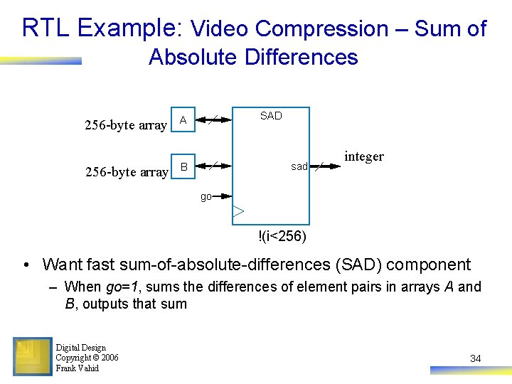
RTL Example: Video Compression – Sum of Absolute Differences 256 -byte array A 256 -byte array B SAD sad integer go !(i<256) • Want fast sum-of-absolute-differences (SAD) component – When go=1, sums the differences of element pairs in arrays A and B, outputs that sum Digital Design Copyright © 2006 Frank Vahid 34

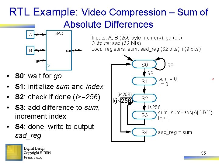
RTL Example: Video Compression – Sum of Absolute Differences SAD A sad B Inputs: A, B (256 byte memory); go (bit) Outputs: sad (32 bits) Local registers: sum, sad_reg (32 bits); i (9 bits) go • • S 0: wait for go S 1: initialize sum and index S 2: check if done (i>=256) S 3: add difference to sum, increment index • S 4: done, write to output sad_reg Digital Design Copyright © 2006 Frank Vahid S 0 go S 1 (i<256)’ !(i<256) !go sum = 0 i=0 a S 2 i<256 sum=sum+abs(A[i]-B[i]) S 3 i=i+1 S 4 sad_reg = sum 35

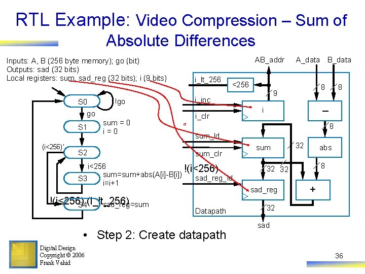
RTL Example: Video Compression – Sum of Absolute Differences AB_addr Inputs: A, B (256 byte memory); go (bit) Outputs: sad (32 bits) Local registers: sum, sad_reg (32 bits); i (9 bits) S 0 i_lt_256 go S 1 (i<256)’ sum = 0 i=0 S 2 <256 i_clr 8 sum_ld sum_clr Datapath • Step 2: Create datapath Digital Design Copyright © 2006 Frank Vahid 8 – i a i<256 !(i<256) sum=sum+abs(A[i]-B[i]) sad_reg_ld S 3 i=i+1 !(i<256) sad_reg=sum S 4(i_lt_256) 8 9 i_inc !go A_data B_data sum 32 abs 8 32 32 sad_reg + 32 sad 36

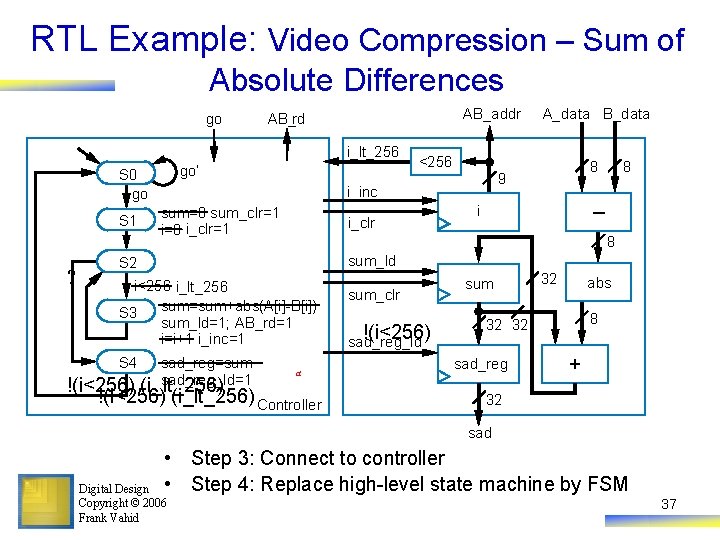
RTL Example: Video Compression – Sum of Absolute Differences go AB_addr AB_rd i_lt_256 go’ S 0 go S 1 ? i_clr 8 9 8 – i 8 sum_ld S 2 i<256 i_lt_256 sum=sum+abs(A[i]-B[i]) S 3 sum_ld=1; AB_rd=1 i=i+1 i_inc=1 S 4 <256 i_inc sum=0 sum_clr=1 i=0 i_clr=1 A_data B_data sad_reg=sum sad_reg_ld=1 (i_lt_256) a !(i<256) (i_lt_256) Controller sum_clr !(i<256) sad_reg_ld sum 32 abs 8 32 32 sad_reg + 32 sad • Step 3: Connect to controller • Step 4: Replace high-level state machine by FSM Digital Design Copyright © 2006 Frank Vahid 37

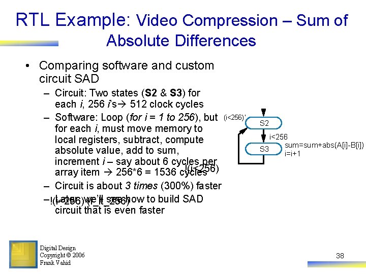
RTL Example: Video Compression – Sum of Absolute Differences • Comparing software and custom circuit SAD – Circuit: Two states (S 2 & S 3) for each i, 256 i’s 512 clock cycles – Software: Loop (for i = 1 to 256), but (i<256)’ for each i, must move memory to local registers, subtract, compute absolute value, add to sum, increment i – say about 6 cycles per !(i<256) array item 256*6 = 1536 cycles – Circuit is about 3 times (300%) faster – !(i<256) Later, we’ll see how to build SAD (i_lt_256) circuit that is even faster Digital Design Copyright © 2006 Frank Vahid S 2 i<256 sum=sum+abs(A[i]-B[i]) S 3 i=i+1 38

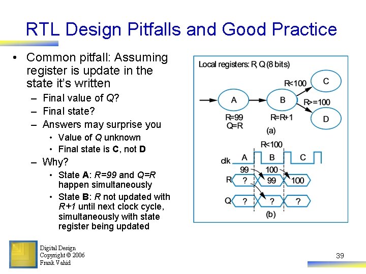
RTL Design Pitfalls and Good Practice • Common pitfall: Assuming register is update in the state it’s written – Final value of Q? – Final state? – Answers may surprise you • Value of Q unknown • Final state is C, not D – Why? • State A: R=99 and Q=R happen simultaneously • State B: R not updated with R+1 until next clock cycle, simultaneously with state register being updated Digital Design Copyright © 2006 Frank Vahid 39

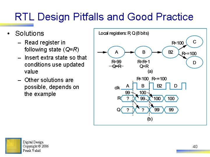
RTL Design Pitfalls and Good Practice • Solutions – Read register in following state (Q=R) – Insert extra state so that conditions use updated value – Other solutions are possible, depends on the example Digital Design Copyright © 2006 Frank Vahid 40

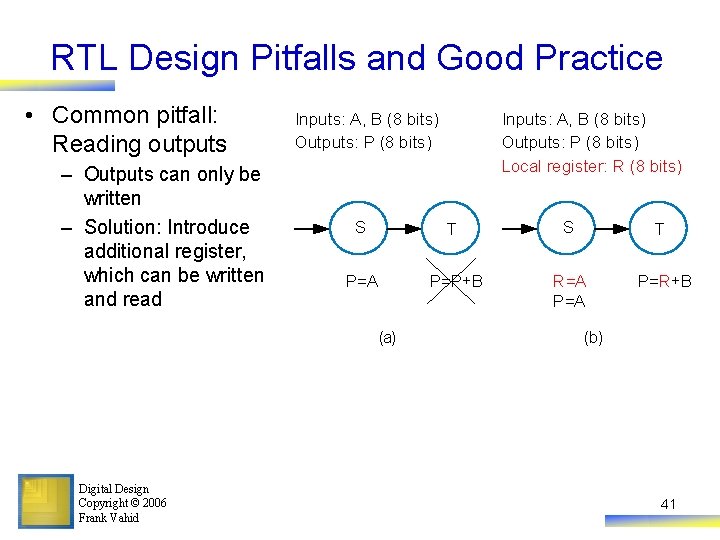
RTL Design Pitfalls and Good Practice • Common pitfall: Reading outputs – Outputs can only be written – Solution: Introduce additional register, which can be written and read Inputs: A, B (8 bits) Outputs: P (8 bits) S T P=A P=P+B R=A P=R+B (a) Digital Design Copyright © 2006 Frank Vahid Inputs: A, B (8 bits) Outputs: P (8 bits) Local register: R (8 bits) (b) 41

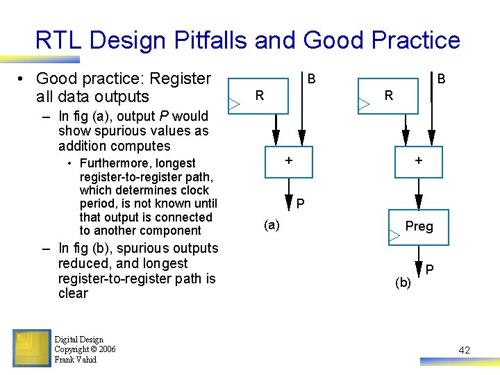
RTL Design Pitfalls and Good Practice • Good practice: Register all data outputs B R – In fig (a), output P would show spurious values as addition computes • Furthermore, longest register-to-register path, which determines clock period, is not known until that output is connected to another component – In fig (b), spurious outputs reduced, and longest register-to-register path is clear Digital Design Copyright © 2006 Frank Vahid B R + + P (a) Preg (b) P 42

Control vs. Data Dominated RTL Design • Designs often categorized as control-dominated or datadominated – Control-dominated design – Controller contains most of the complexity – Data-dominated design – Datapath contains most of the complexity – General, descriptive terms – no hard rule that separates the two types of designs – Laser-based distance measurer – control dominated – Bus interface, SAD circuit – mix of control and data – Now let’s do a data dominated design Digital Design Copyright © 2006 Frank Vahid 43

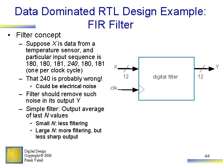
Data Dominated RTL Design Example: FIR Filter • Filter concept – Suppose X is data from a temperature sensor, and particular input sequence is 180, 181, 240, 181 (one per clock cycle) – That 240 is probably wrong! • Could be electrical noise – Filter should remove such noise in its output Y – Simple filter: Output average of last N values Y X 12 digital filter 12 clk • Small N: less filtering • Large N: more filtering, but less sharp output Digital Design Copyright © 2006 Frank Vahid 44

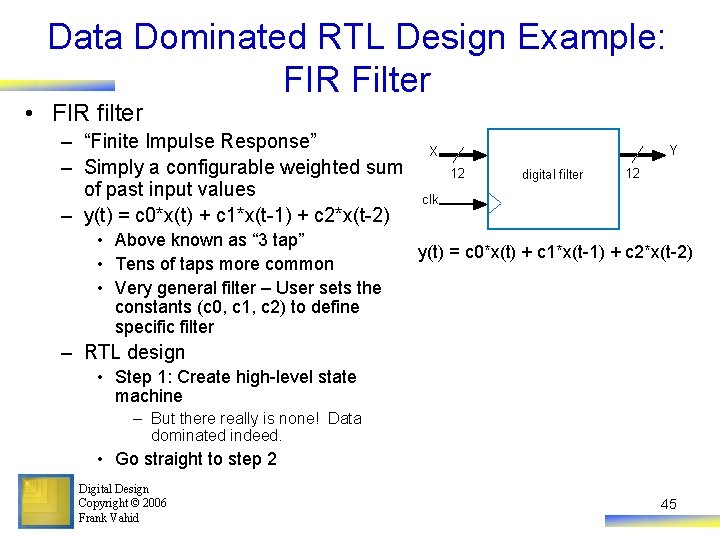
Data Dominated RTL Design Example: FIR Filter • FIR filter – “Finite Impulse Response” – Simply a configurable weighted sum of past input values – y(t) = c 0*x(t) + c 1*x(t-1) + c 2*x(t-2) • Above known as “ 3 tap” • Tens of taps more common • Very general filter – User sets the constants (c 0, c 1, c 2) to define specific filter Y X 12 digital filter 12 clk y(t) = c 0*x(t) + c 1*x(t-1) + c 2*x(t-2) – RTL design • Step 1: Create high-level state machine – But there really is none! Data dominated indeed. • Go straight to step 2 Digital Design Copyright © 2006 Frank Vahid 45

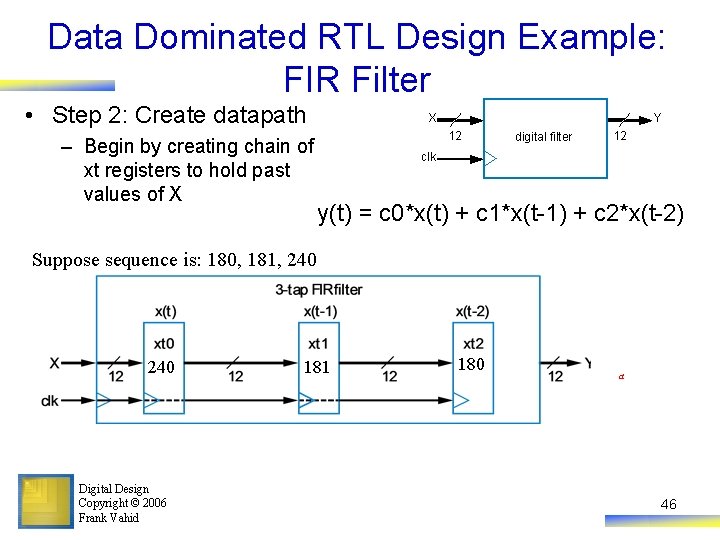
Data Dominated RTL Design Example: FIR Filter • Step 2: Create datapath – Begin by creating chain of xt registers to hold past values of X Y X 12 digital filter 12 clk y(t) = c 0*x(t) + c 1*x(t-1) + c 2*x(t-2) Suppose sequence is: 180, 181, 240 180 181 Digital Design Copyright © 2006 Frank Vahid 180 181 180 a 46

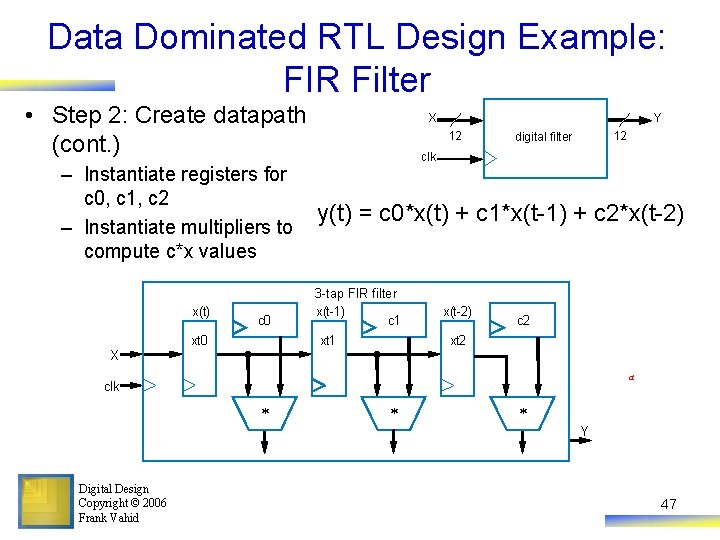
Data Dominated RTL Design Example: FIR Filter • Step 2: Create datapath (cont. ) – Instantiate registers for c 0, c 1, c 2 – Instantiate multipliers to compute c*x values x(t) c 0 xt 0 Y X 12 12 digital filter clk y(t) = c 0*x(t) + c 1*x(t-1) + c 2*x(t-2) 3 -tap FIR filter x(t-1) c 1 xt 1 x(t-2) c 2 xt 2 X a clk * * * Y Digital Design Copyright © 2006 Frank Vahid 47

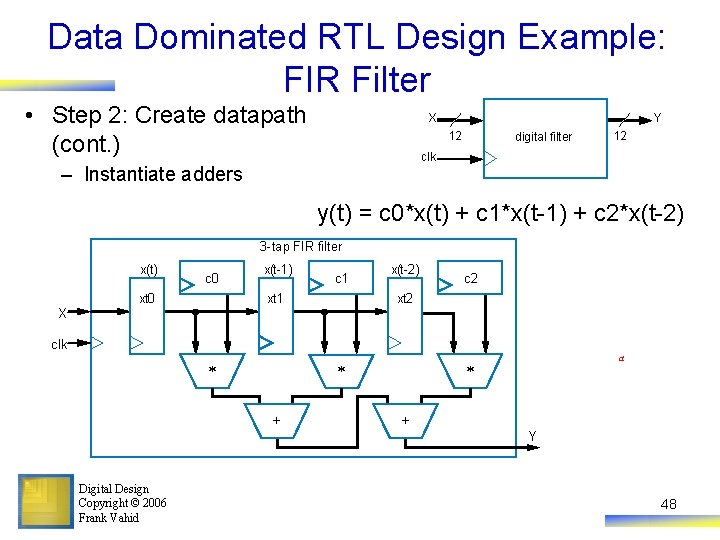
Data Dominated RTL Design Example: FIR Filter • Step 2: Create datapath (cont. ) Y X 12 digital filter 12 clk – Instantiate adders y(t) = c 0*x(t) + c 1*x(t-1) + c 2*x(t-2) 3 -tap FIR filter x(t) c 0 xt 0 x(t-1) c 1 xt 1 x(t-2) c 2 xt 2 X clk * * + Digital Design Copyright © 2006 Frank Vahid a * + Y 48

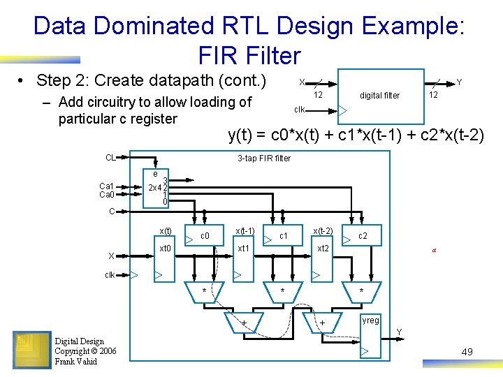
Data Dominated RTL Design Example: FIR Filter • Step 2: Create datapath (cont. ) Y X 12 – Add circuitry to allow loading of particular c register digital filter 12 clk y(t) = c 0*x(t) + c 1*x(t-1) + c 2*x(t-2) CL 3 -tap FIR filter e Ca 1 Ca 0 3 2 x 4 2 1 0 C x(t) X c 0 xt 0 x(t-1) c 1 xt 1 x(t-2) c 2 xt 2 a clk * * + Digital Design Copyright © 2006 Frank Vahid * + yreg Y 49

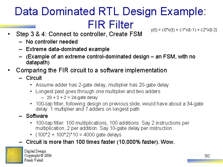
Data Dominated RTL Design Example: FIR Filter • Step 3 & 4: Connect to controller, Create FSM y(t) = c 0*x(t) + c 1*x(t-1) + c 2*x(t-2) – No controller needed – Extreme data-dominated example – (Example of an extreme control-dominated design – an FSM, with no datapath) • Comparing the FIR circuit to a software implementation – Circuit • Assume adder has 2 -gate delay, multiplier has 20 -gate delay • Longest past goes through one multiplier and two adders – 20 + 2 = 24 -gate delay • 100 -tap filter, following design on previous slide, would have about a 34 -gate delay: 1 multiplier and 7 adders on longest path – Software • 100 -tap filter: 100 multiplications, 100 additions. Say 2 instructions per multiplication, 2 per addition. Say 10 -gate delay per instruction. • (100*2 + 100*2)*10 = 4000 gate delays – Circuit is more than 100 times faster (10, 000% faster). Wow. Digital Design Copyright © 2006 Frank Vahid 50

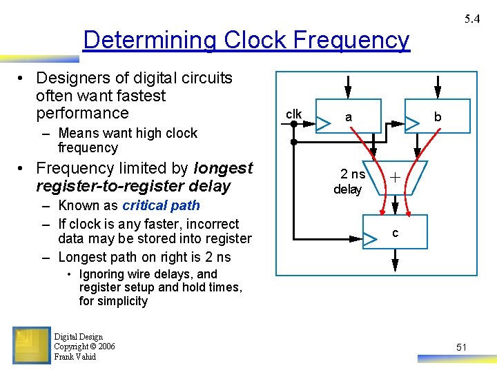
5. 4 Determining Clock Frequency • Designers of digital circuits often want fastest performance clk a b – Means want high clock frequency • Frequency limited by longest register-to-register delay – Known as critical path – If clock is any faster, incorrect data may be stored into register – Longest path on right is 2 ns delay + c • Ignoring wire delays, and register setup and hold times, for simplicity Digital Design Copyright © 2006 Frank Vahid 51

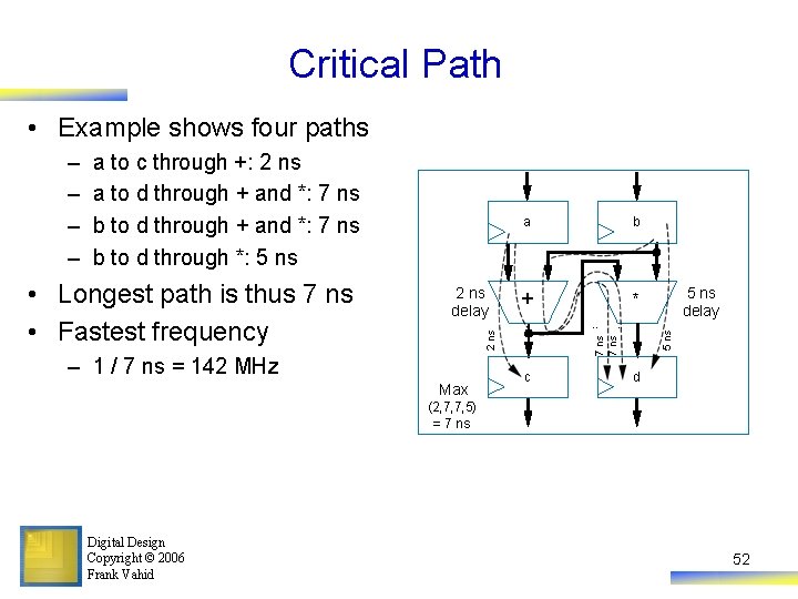
Critical Path • Example shows four paths 2 ns delay b + * 7 ns – 1 / 7 ns = 142 MHz Max c 5 ns delay 7 ns • Longest path is thus 7 ns • Fastest frequency a 5 ns a to c through +: 2 ns a to d through + and *: 7 ns b to d through *: 5 ns 2 ns – – d (2, 7, 7, 5) = 7 ns Digital Design Copyright © 2006 Frank Vahid 52

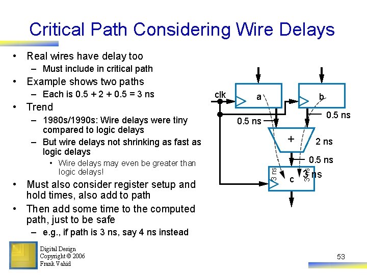
Critical Path Considering Wire Delays • Real wires have delay too – Must include in critical path • Example shows two paths – 1980 s/1990 s: Wire delays were tiny compared to logic delays – But wire delays not shrinking as fast as logic delays • Wire delays may even be greater than logic delays! • Must also consider register setup and hold times, also add to path • Then add some time to the computed path, just to be safe a b 0. 5 ns + 2 ns 0. 5 ns 3 ns • Trend clk 3 ns – Each is 0. 5 + 2 + 0. 5 = 3 ns c 3 ns – e. g. , if path is 3 ns, say 4 ns instead Digital Design Copyright © 2006 Frank Vahid 53

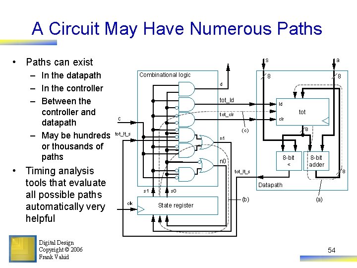
A Circuit May Have Numerous Paths • Paths can exist – In the datapath – In the controller – Between the controller and datapath – May be hundreds or thousands of paths • Timing analysis tools that evaluate all possible paths automatically very helpful Digital Design Copyright © 2006 Frank Vahid s Combinational logic a 8 8 d tot_ld ld tot t ot_clr c clr 8 (c) tot_lt_s n 1 8 -bit < n 0 8 -bit adder 8 tot_lt_s s 1 clk Datapath s 0 State register (b) (a) 54

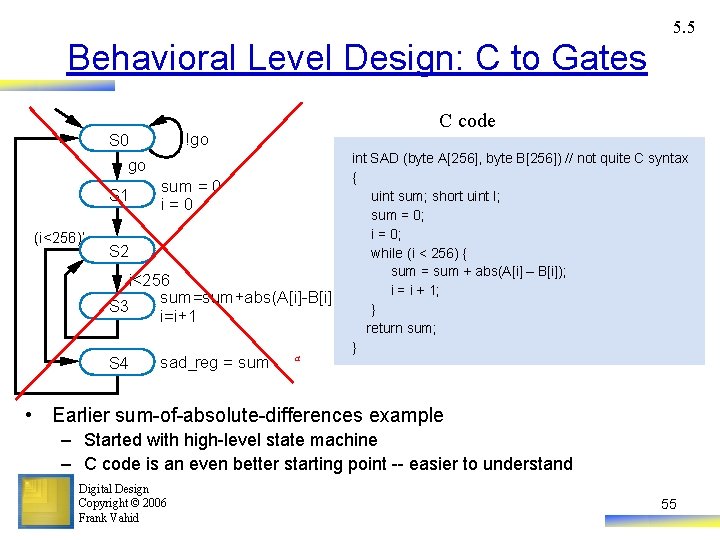
5. 5 Behavioral Level Design: C to Gates !go S 0 go S 1 (i<256)’ C code sum = 0 i=0 S 2 i<256 sum=sum+abs(A[i]-B[i]) S 3 i=i+1 S 4 sad_reg = sum a int SAD (byte A[256], byte B[256]) // not quite C syntax { uint sum; short uint I; sum = 0; i = 0; while (i < 256) { sum = sum + abs(A[i] – B[i]); i = i + 1; } return sum; } • Earlier sum-of-absolute-differences example – Started with high-level state machine – C code is an even better starting point -- easier to understand Digital Design Copyright © 2006 Frank Vahid 55

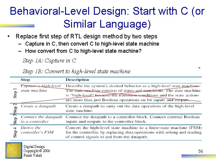
Behavioral-Level Design: Start with C (or Similar Language) • Replace first step of RTL design method by two steps – Capture in C, then convert C to high-level state machine – How convert from C to high-level state machine? Step 1 A: Capture in C Step 1 B: Convert to high-level state machine Digital Design Copyright © 2006 Frank Vahid a 56

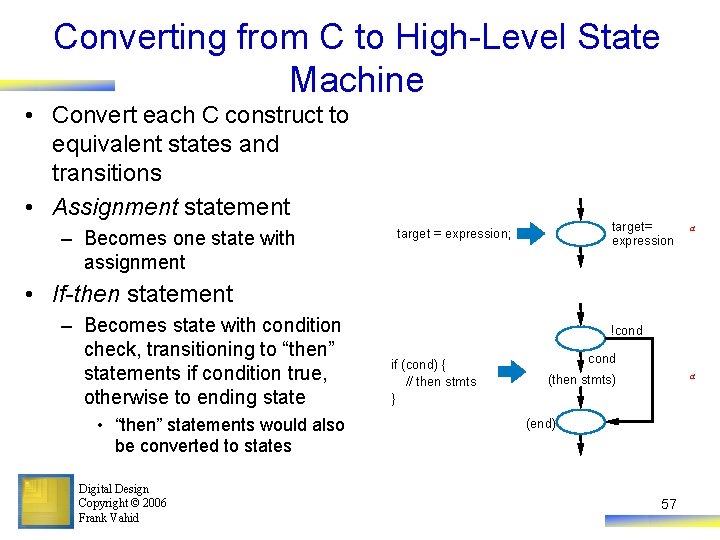
Converting from C to High-Level State Machine • Convert each C construct to equivalent states and transitions • Assignment statement – Becomes one state with assignment target= expression target = expression; a • If-then statement – Becomes state with condition check, transitioning to “then” statements if condition true, otherwise to ending state • “then” statements would also be converted to states Digital Design Copyright © 2006 Frank Vahid !cond if (cond) { // then stmts } cond a (then stmts) (end) 57

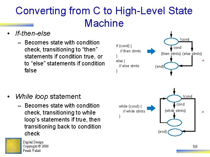
Converting from C to High-Level State Machine • If-then-else – Becomes state with condition check, transitioning to “then” statements if condition true, or to “else” statements if condition false !cond if (cond) { // then stmts } else { // else stmts } cond (then stmts) (else stmts) a (end) • While loop statement – Becomes state with condition check, transitioning to while loop’s statements if true, then transitioning back to condition check Digital Design Copyright © 2006 Frank Vahid !cond while (cond) { // while stmts } cond (while stmts) a (end) 58

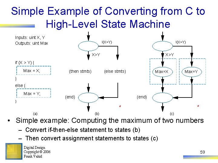
Simple Example of Converting from C to High-Level State Machine Inputs: uint X, Y Outputs: uint Max !(X>Y) X>Y if (X > Y) { Max = X; (then stmts) (else stmts) Max=X Max=Y } else { Max = Y; } (end) a a (a) (b) (c) • Simple example: Computing the maximum of two numbers – Convert if-then-else statement to states (b) – Then convert assignment statements to states (c) Digital Design Copyright © 2006 Frank Vahid 59

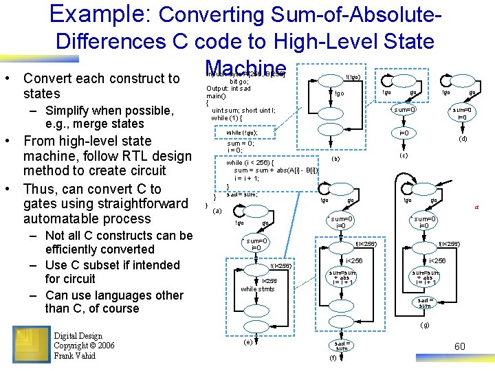
Example: Converting Sum-of-Absolute • Differences C code to High-Level State Machine Convert each construct to states – Simplify when possible, e. g. , merge states • From high-level state machine, follow RTL design method to create circuit • Thus, can convert C to gates using straightforward automatable process – Not all C constructs can be efficiently converted – Use C subset if intended for circuit – Can use languages other than C, of course Inputs: byte A[256, B[256] bit go; Output: int sad main() { uint sum; short uint I; while (1) { !(!go) !go sad = sum; !go (d) (c) (b) while (i < 256) { sum = sum + abs(A[i] - B[i]); i = i + 1; } go sum=0 i=0 sum = 0; i = 0; } !go sum=0 while (!go); } go go !go go a (a) !go sum=0 i=0 !(i<256) i<256 while stmts sum=sum + abs i=i+1 !(i<256) i<256 sum=sum + abs i=i+1 sad = sum (g) Digital Design Copyright © 2006 Frank Vahid (e) sad = sum (f) 60

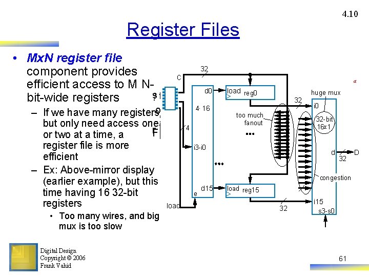
4. 10 Register Files • Mx. N register file component provides er C C efficient access to M N- er t s ompu t ? bit-wide registers 32 8 d 0 d 0 ompu 4× 162× 4 cthe car – If we have many registersom a com rt l the car's d 1 r but only need access oneal rt F n 4 a 0 e c r i 0 Fn e or two at a time, a c i 1 register file is more i 3 -i 0 a 1 d 2 efficient – Ex: Above-mirror display (earlier example), but this d 3 d 15 e time having 16 32 -bit e load registers load • Too many wires, and big mux is too slow Digital Design Copyright © 2006 Frank Vahid a load reg 0 too much fanout load reg 1 huge mux T 32 8 A 8 load reg 2 I 32 8 load reg 3 load reg 15 o th or mi dis T mi T r rorod 32 -bit 8 -bit r 16 x 41× 1 r o i 1 ve a o y a ve d d y - DD 8 i 0 i 2 congestion M 32 8 i 15 i 3 s 1 s 0 s 3 -s 0 x y 61

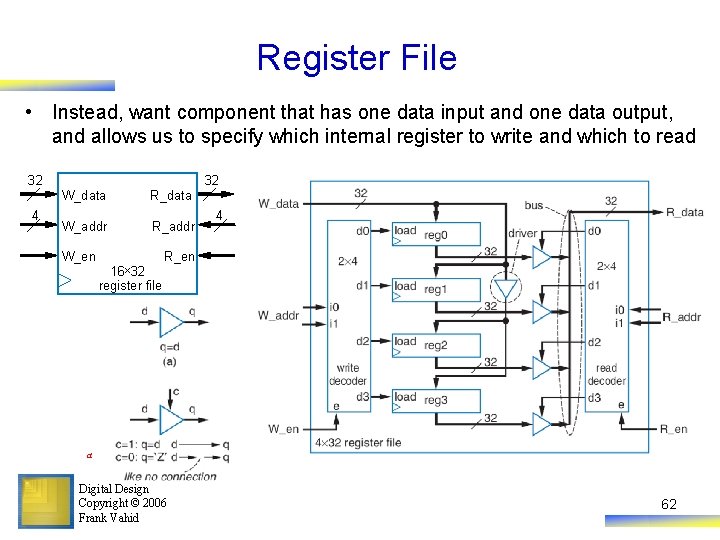
Register File • Instead, want component that has one data input and one data output, and allows us to specify which internal register to write and which to read 32 4 32 W_data R_data W_addr R_addr W_en 16× 32 register file a 4 R_en a Digital Design Copyright © 2006 Frank Vahid 62

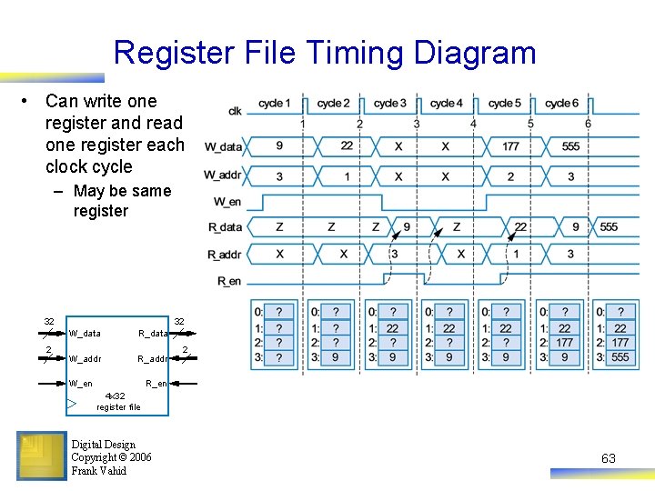
Register File Timing Diagram • Can write one register and read one register each clock cycle – May be same register 32 2 32 W_data R_data W_addr R_addr W_en 2 R_en 4 x 32 register file Digital Design Copyright © 2006 Frank Vahid 63

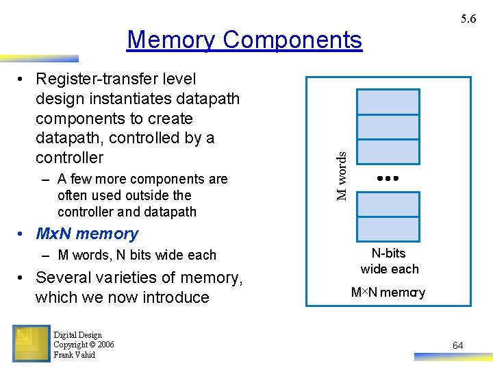
5. 6 • Register-transfer level design instantiates datapath components to create datapath, controlled by a controller – A few more components are often used outside the controller and datapath M words Memory Components • Mx. N memory – M words, N bits wide each • Several varieties of memory, which we now introduce Digital Design Copyright © 2006 Frank Vahid N-bits wide each M×N memory 64

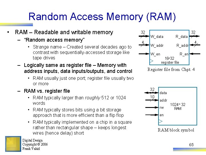
Random Access Memory (RAM) • RAM – Readable and writable memory – “Random access memory” • Strange name – Created several decades ago to contrast with sequentially-accessed storage like tape drives – Logically same as register file – Memory with address inputs, data inputs/outputs, and control 32 4 32 W_data R_data W_addr R_addr W_en 16× 32 register file 4 R_en Register file from Chpt. 4 • RAM usually just one port; register file usually two or more – RAM vs. register file • RAM typically larger than roughly 512 or 1024 words • RAM typically stores bits using a bit storage approach that is more efficient than a flip flop • RAM typically implemented on a chip in a square rather than rectangular shape – keeps longest wires (hence delay) short Digital Design Copyright © 2006 Frank Vahid 32 10 data addr rw 1024× 32 RAM en RAM block symbol 65

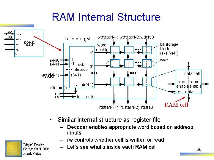
RAM Internal Structure 32 10 data addr rw Let A = log 2 M 1024 x 32 RAM en d 0 addr 1 addr(A-1) addr clk en rw wdata(N-1) wdata(N-2) wdata 0 word enable a 0 a 1 Ax. M d 1 decoder a(A-1) e bit storage block (aka “cell”) word data cell word enable rw data d(M-1) to all cells rdata(N-1) rdata(N-2) rdata 0 RAM cell • Similar internal structure as register file Digital Design Copyright © 2006 Frank Vahid – Decoder enables appropriate word based on address inputs – rw controls whether cell is written or read – Let’s see what’s inside each RAM cell 66

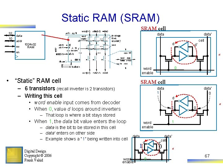
Static RAM (SRAM) SRAM cell 32 10 data addr rw data’ cell d 1024 x 32 RAM d’ en a 0 word enable • “Static” RAM cell SRAM cell – 6 transistors (recall inverter is 2 transistors) – Writing this cell data 1 data’ 0 d • word enable input comes from decoder • When 0, value d loops around inverters a 1 0 – That loop is where a bit stays stored • When 1, the data bit value enters the loop – data is the bit to be stored in this cell – data’ enters on other side – Example shows a “ 1” being written into cell data 1 Digital Design Copyright © 2006 Frank Vahid 1 word enable d 0 data’ cell d’ 0 a 67

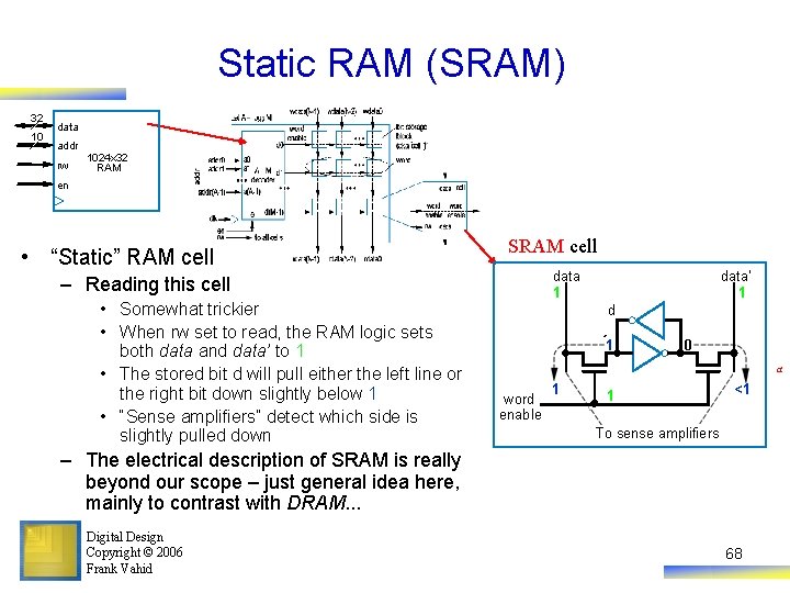
Static RAM (SRAM) 32 10 data addr rw 1024 x 32 RAM en • “Static” RAM cell SRAM cell data 1 – Reading this cell • Somewhat trickier • When rw set to read, the RAM logic sets both data and data’ to 1 • The stored bit d will pull either the left line or the right bit down slightly below 1 • “Sense amplifiers” detect which side is slightly pulled down data’ 1 d 1 0 a word enable 1 1 <1 To sense amplifiers – The electrical description of SRAM is really beyond our scope – just general idea here, mainly to contrast with DRAM. . . Digital Design Copyright © 2006 Frank Vahid 68

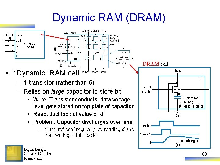
Dynamic RAM (DRAM) 32 10 data addr rw 1024 x 32 RAM en DRAM cell • “Dynamic” RAM cell – 1 transistor (rather than 6) – Relies on large capacitor to store bit • Write: Transistor conducts, data voltage level gets stored on top plate of capacitor • Read: Just look at value of d • Problem: Capacitor discharges over time – Must “refresh” regularly, by reading d and then writing it right back data cell word enable capacitor slowly discharging (a) data enable d Digital Design Copyright © 2006 Frank Vahid d (b) discharges 69

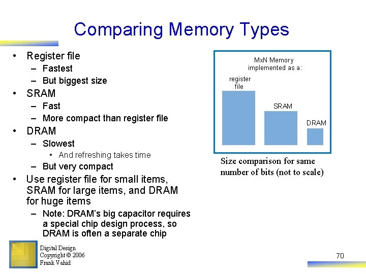
Comparing Memory Types • Register file – Fastest – But biggest size • SRAM – Fast – More compact than register file • DRAM Mx. N Memory implemented as a: register file SRAM DRAM – Slowest • And refreshing takes time – But very compact • Use register file for small items, SRAM for large items, and DRAM for huge items Size comparison for same number of bits (not to scale) – Note: DRAM’s big capacitor requires a special chip design process, so DRAM is often a separate chip Digital Design Copyright © 2006 Frank Vahid 70

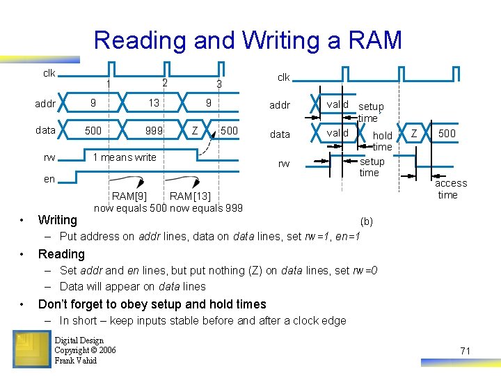
Reading and Writing a RAM clk 2 1 addr 9 13 data 500 999 rw 3 9 Z addr 500 1 means write en • Writing clk data rw valid setup time valid hold time setup time RAM[9] RAM[13] now equals 500 now equals 999 Z 500 access time (b) – Put address on addr lines, data on data lines, set rw=1, en=1 • Reading – Set addr and en lines, but put nothing (Z) on data lines, set rw=0 – Data will appear on data lines • Don’t forget to obey setup and hold times – In short – keep inputs stable before and after a clock edge Digital Design Copyright © 2006 Frank Vahid 71

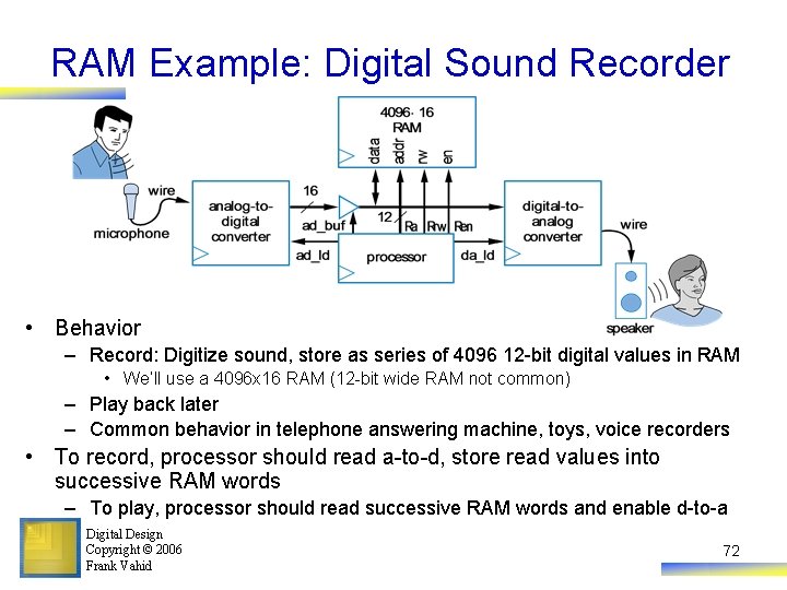
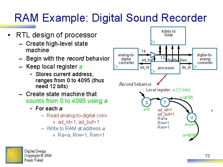
RAM Example: Digital Sound Recorder • Behavior – Record: Digitize sound, store as series of 4096 12 -bit digital values in RAM • We’ll use a 4096 x 16 RAM (12 -bit wide RAM not common) – Play back later – Common behavior in telephone answering machine, toys, voice recorders • To record, processor should read a-to-d, store read values into successive RAM words – To play, processor should read successive RAM words and enable d-to-a Digital Design Copyright © 2006 Frank Vahid 72

RAM Example: Digital Sound Recorder 4096 x 16 RAM • RTL design of processor – Create high-level state machine – Begin with the record behavior – Keep local register a • Stores current address, ranges from 0 to 4095 (thus need 12 bits) – Create state machine that counts from 0 to 4095 using a • For each a – Read analog-to-digital conv. » ad_ld=1, ad_buf=1 – Write to RAM at address a » Ra=a, Rrw=1, Ren=1 Digital Design Copyright © 2006 Frank Vahid analog-todigital converter 16 ad_buf ad_ld 12 digital-toanalog converter Ra Rw Ren processor da_ld Record behavior Local register: a (12 bits) a<4095 S T a=0 ad_ld=1 ad_buf=1 Ra=a Rrw=1 Ren=1 a U a=a+1 a=4095 73

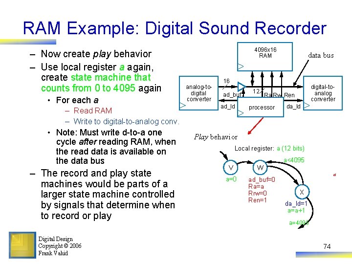
RAM Example: Digital Sound Recorder – Now create play behavior – Use local register a again, create state machine that counts from 0 to 4095 again • For each a – Read RAM – Write to digital-to-analog conv. • Note: Must write d-to-a one cycle after reading RAM, when the read data is available on the data bus – The record and play state machines would be parts of a larger state machine controlled by signals that determine when to record or play Digital Design Copyright © 2006 Frank Vahid 4096 x 16 RAM analog-todigital converter data bus 16 ad_buf ad_ld 12 digital-toanalog converter Ra Rw Ren processor da_ld Play behavior Local register: a (12 bits) a<4095 V W a=0 ad_buf=0 Ra=a Rrw=0 Ren=1 a X da_ld=1 a=a+1 a=4095 74

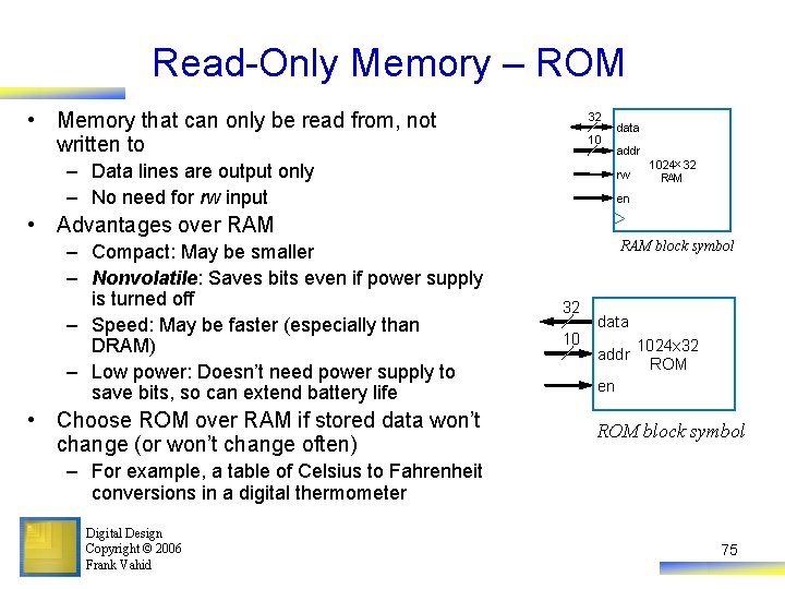
Read-Only Memory – ROM • Memory that can only be read from, not written to 32 10 – Data lines are output only – No need for rw input data addr rw 1024× 32 RAM en • Advantages over RAM – Compact: May be smaller – Nonvolatile: Saves bits even if power supply is turned off – Speed: May be faster (especially than DRAM) – Low power: Doesn’t need power supply to save bits, so can extend battery life • Choose ROM over RAM if stored data won’t change (or won’t change often) RAM block symbol 32 10 data addr 1024 x 32 ROM en ROM block symbol – For example, a table of Celsius to Fahrenheit conversions in a digital thermometer Digital Design Copyright © 2006 Frank Vahid 75

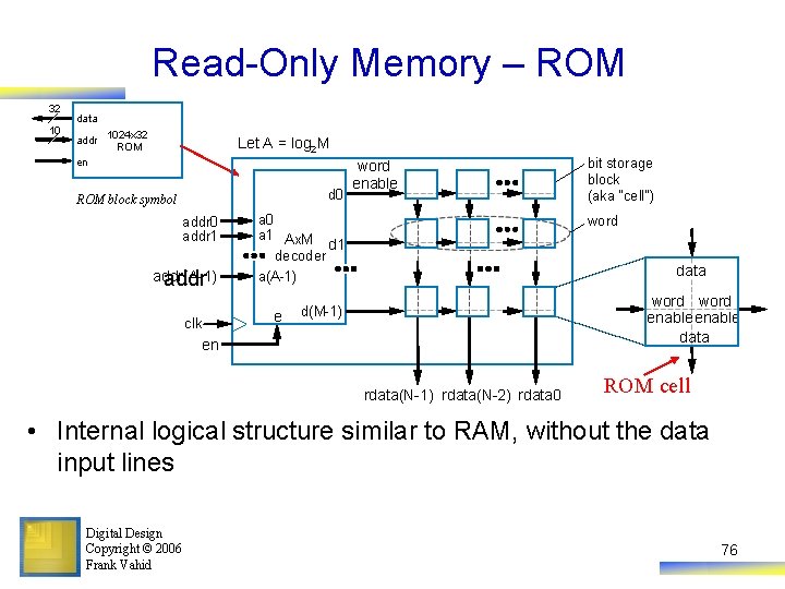
Read-Only Memory – ROM 32 10 data addr 1024 x 32 ROM en Let A = log 2 M d 0 ROM block symbol addr 0 addr 1 addr(A-1) addr clk word enable a 0 a 1 Ax. M d 1 decoder a(A-1) e bit storage block (aka “cell”) word data word enable data d(M-1) en rdata(N-1) rdata(N-2) rdata 0 ROM cell • Internal logical structure similar to RAM, without the data input lines Digital Design Copyright © 2006 Frank Vahid 76

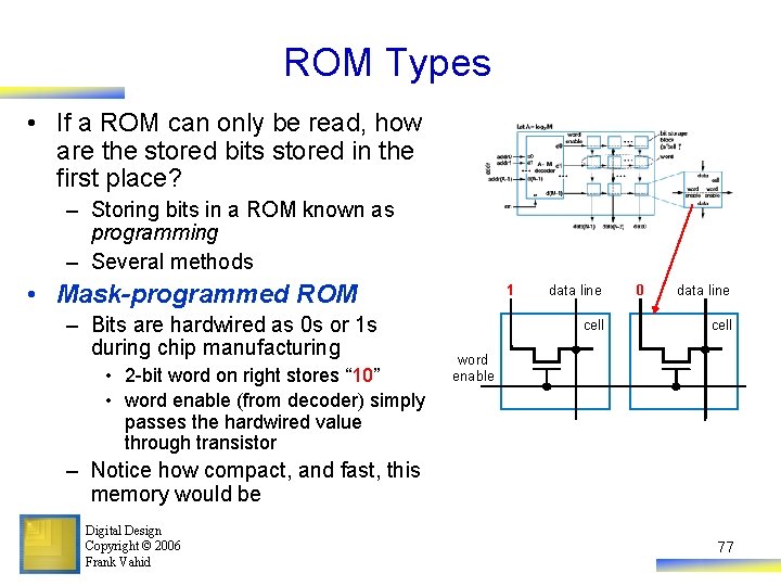
ROM Types • If a ROM can only be read, how are the stored bits stored in the first place? – Storing bits in a ROM known as programming – Several methods • Mask-programmed ROM – Bits are hardwired as 0 s or 1 s during chip manufacturing • 2 -bit word on right stores “ 10” • word enable (from decoder) simply passes the hardwired value through transistor 1 data line cell 0 data line cell word enable – Notice how compact, and fast, this memory would be Digital Design Copyright © 2006 Frank Vahid 77

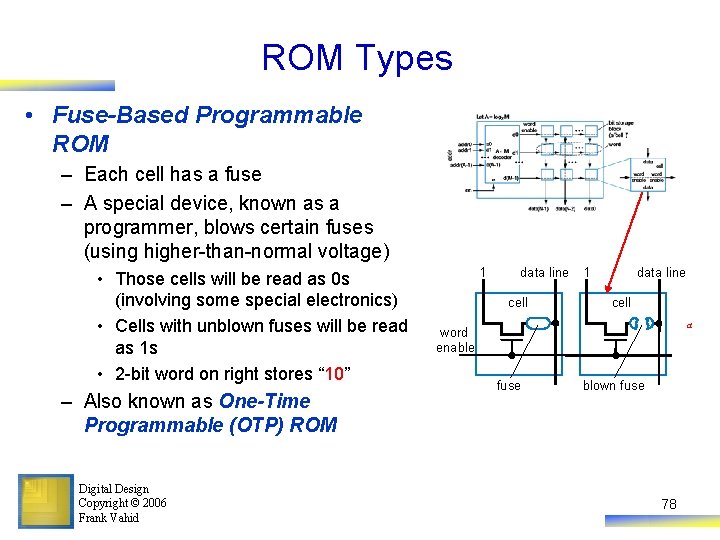
ROM Types • Fuse-Based Programmable ROM – Each cell has a fuse – A special device, known as a programmer, blows certain fuses (using higher-than-normal voltage) • Those cells will be read as 0 s (involving some special electronics) • Cells with unblown fuses will be read as 1 s • 2 -bit word on right stores “ 10” – Also known as One-Time Programmable (OTP) ROM Digital Design Copyright © 2006 Frank Vahid 1 data line cell a word enable fuse blown fuse 78

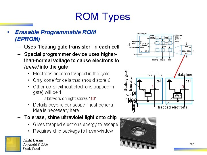
ROM Types • Erasable Programmable ROM (EPROM) • Electrons become trapped in the gate • Only done for cells that should store 0 • Other cells (without electrons trapped in gate) will be 1 – 2 -bit word on right stores “ 10” • Details beyond our scope – just general idea is necessary here floating-gate transistor – Uses “floating-gate transistor” in each cell – Special programmer device uses higherthan-normal voltage to cause electrons to tunnel into the gate o tr word enable ting ar e ta t g data line cell 1 0 eÐeÐ trapped electrons – To erase, shine ultraviolet light onto chip • Gives trapped electrons energy to escape • Requires chip package to have window Digital Design Copyright © 2006 Frank Vahid 79

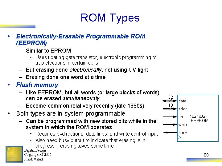
ROM Types • Electronically-Erasable Programmable ROM (EEPROM) – Similar to EPROM • Uses floating-gate transistor, electronic programming to trap electrons in certain cells – But erasing done electronically, not using UV light – Erasing done word at a time • Flash memory – Like EEPROM, but all words (or large blocks of words) can be erased simultaneously – Become common relatively recently (late 1990 s) • Both types are in-system programmable – Can be programmed with new stored bits while in the system in which the ROM operates • Requires bi-directional data lines, and write control input • Also need busy output to indicate that erasing is in progress – erasing takes some time Digital Design Copyright © 2006 Frank Vahid 32 10 data addr en write 1024 x 32 EEPROM busy 80

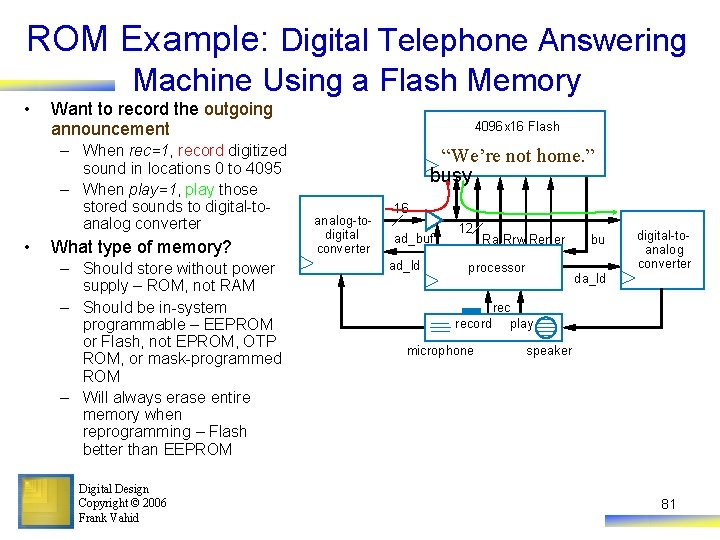
ROM Example: Digital Telephone Answering Machine Using a Flash Memory • Want to record the outgoing announcement – When rec=1, record digitized sound in locations 0 to 4095 – When play=1, play those stored sounds to digital-toanalog converter • What type of memory? – Should store without power supply – ROM, not RAM – Should be in-system programmable – EEPROM or Flash, not EPROM, OTP ROM, or mask-programmed ROM – Will always erase entire memory when reprogramming – Flash better than EEPROM Digital Design Copyright © 2006 Frank Vahid 4096 x 16 Flash “We’re not home. ” busy analog-todigital converter 16 ad_buf ad_ld 12 Ra Rrw Rener processor record microphone bu digital-toanalog converter da_ld rec play speaker 81

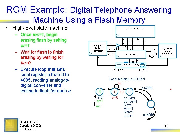
ROM Example: Digital Telephone Answering Machine Using a Flash Memory • High-level state machine – Once rec=1, begin erasing flash by setting er=1 – Wait for flash to finish erasing by waiting for bu=0 – Execute loop that sets local register a from 0 to 4095, reading analog-todigital converter and writing to flash for each a 4096 x 16 Flash analog-todigital converter ad_buf 12 ad_ld Ra Rrw Ren er processor bu da_ld digital-toanalog converter record play microphone S a=0 er=1 rec Digital Design Copyright © 2006 Frank Vahid 16 speaker Local register: a (13 bits) bu a<4096 T bu’ U er=0 ad_ld=1 ad_buf=1 Ra=a Rrw=1 Ren=1 a=a+1 a V a=4096 82

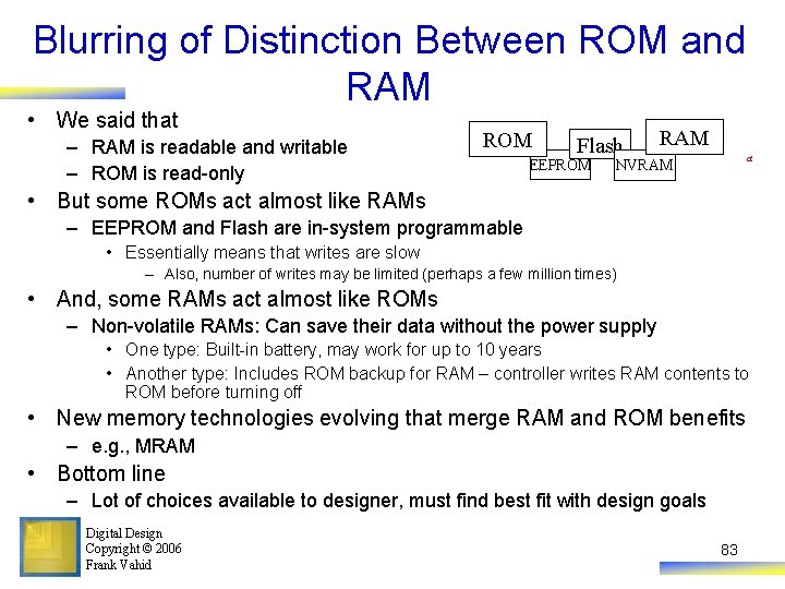
Blurring of Distinction Between ROM and RAM • We said that – RAM is readable and writable – ROM is read-only ROM Flash EEPROM RAM a NVRAM • But some ROMs act almost like RAMs – EEPROM and Flash are in-system programmable • Essentially means that writes are slow – Also, number of writes may be limited (perhaps a few million times) • And, some RAMs act almost like ROMs – Non-volatile RAMs: Can save their data without the power supply • One type: Built-in battery, may work for up to 10 years • Another type: Includes ROM backup for RAM – controller writes RAM contents to ROM before turning off • New memory technologies evolving that merge RAM and ROM benefits – e. g. , MRAM • Bottom line – Lot of choices available to designer, must find best fit with design goals Digital Design Copyright © 2006 Frank Vahid 83

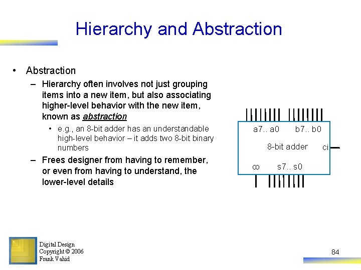
Hierarchy and Abstraction • Abstraction – Hierarchy often involves not just grouping items into a new item, but also associating higher-level behavior with the new item, known as abstraction • e. g. , an 8 -bit adder has an understandable high-level behavior – it adds two 8 -bit binary numbers – Frees designer from having to remember, or even from having to understand, the lower-level details Digital Design Copyright © 2006 Frank Vahid a 7. . a 0 b 7. . b 0 8 -bit adder co ci s 7. . s 0 84

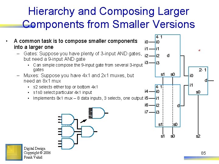
Hierarchy and Composing Larger Components from Smaller Versions • A common task is to compose smaller components into a larger one – Gates: Suppose you have plenty of 3 -input AND gates, but need a 9 -input AND gate a • Can simple compose the 9 -input gate from several 3 -input gates – Muxes: Suppose you have 4 x 1 and 2 x 1 muxes, but need an 8 x 1 mux • s 2 selects either top or bottom 4 x 1 • s 1 s 0 select particular 4 x 1 input • Implements 8 x 1 mux – 8 data inputs, 3 selects, one output P ro vin ce 1 Digital Design Copyright © 2006 Frank Vahid 85

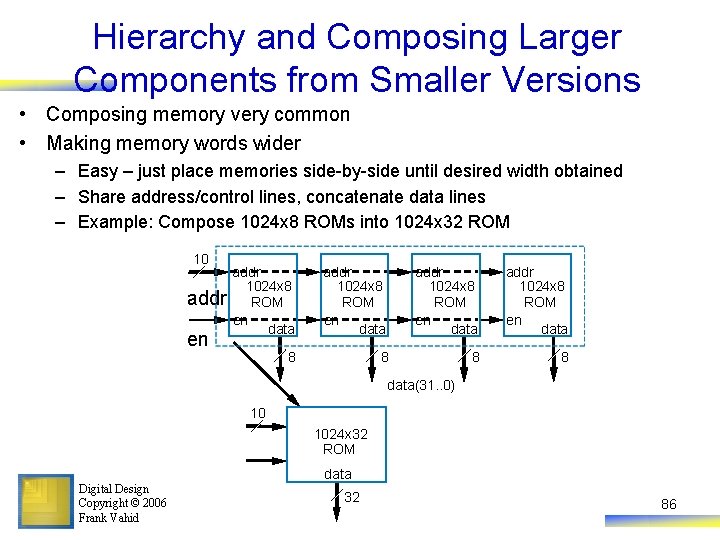
Hierarchy and Composing Larger Components from Smaller Versions • Composing memory very common • Making memory words wider – Easy – just place memories side-by-side until desired width obtained – Share address/control lines, concatenate data lines – Example: Compose 1024 x 8 ROMs into 1024 x 32 ROM 10 addr en addr 1024 x 8 ROM en data 8 8 data(31. . 0) 10 1024 x 32 ROM data Digital Design Copyright © 2006 Frank Vahid 32 86

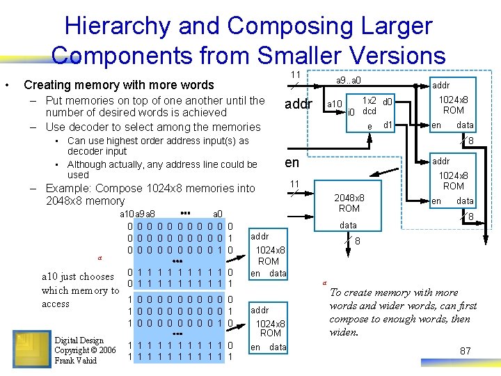
Hierarchy and Composing Larger Components from Smaller Versions • 11 Creating memory with more words – Put memories on top of one another until the number of desired words is achieved – Use decoder to select among the memories • Can use highest order address input(s) as decoder input • Although actually, any address line could be used addr a a 10 just chooses 0 1 1 1 1 1 0 0 1 1 1 1 1 which memory to 1 0 0 0 0 0 access 1 0 0 0 0 0 1 1 0 0 0 0 1 0 Digital Design Copyright © 2006 Frank Vahid 1 1 1 1 1 0 1 1 1 a 10 1 x 2 d 0 dcd i 0 e d 1 addr 1024 x 8 ROM en data 8 en – Example: Compose 1024 x 8 memories into 2048 x 8 memory a 10 a 9 a 8 a 0 0 0 0 0 0 1 0 0 0 0 0 1 0 a 9. . a 0 addr 1024 x 8 ROM 11 2048 x 8 ROM data addr 1024 x 8 ROM en data 8 8 a addr 1024 x 8 ROM en data en To create memory with more words and wider words, can first compose to enough words, then widen. 87

Chapter Summary – Modern digital design involves creating processor-level components – Four-step RTL method can be used • 1. High-level state machine 2. Create datapath 3. Connect datapath to controller 4. Derive controller FSM – Several example • Control dominated, data dominated, and mix – Determining fastest clock frequency • By finding critical path – Behavioral-level design – C to gates • By using method to convert C (subset) to high-level state machine – Additional RTL components • Memory: RAM, ROM • Queues – Hierarchy: A key concept used throughout Chapters 2 -5 Digital Design Copyright © 2006 Frank Vahid 88