
OFDM Transceiver using HDL PA U L PETHS
- Slides: 41
OFDM Transceiver using HDL PA U L PETHS OMVONG ZACH ASAL DR. I N SOO AHN DR. YUFEN G LU MAY 6, 2014
Outline • Project Overview • Project Goal • Project Description • Orthogonal Frequency Division Multiplexing (OFDM) • Communication Channel Effect • Specifications • Results • Conclusion • References 2
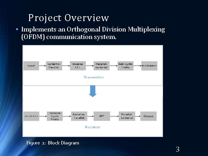
Project Overview • Implements an Orthogonal Division Multiplexing (OFDM) communication system. Figure 1: Block Diagram 3
Project Goal • To implement a complete OFDM system using field programmable gate arrays (FPGA) and VHDL hardware description language. The OFDM system can be reconfigurable. 4
Project Description • The project is divided into three stages. • Stage 1: MATLAB/Simulink • Stage 2: FPGA board implementation with channel effects 5
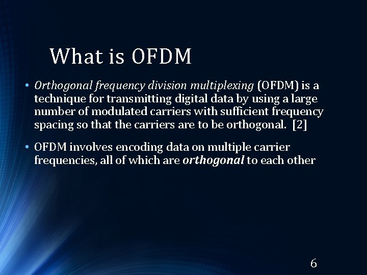
What is OFDM • Orthogonal frequency division multiplexing (OFDM) is a technique for transmitting digital data by using a large number of modulated carriers with sufficient frequency spacing so that the carriers are to be orthogonal. [2] • OFDM involves encoding data on multiple carrier frequencies, all of which are orthogonal to each other 6
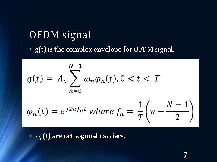
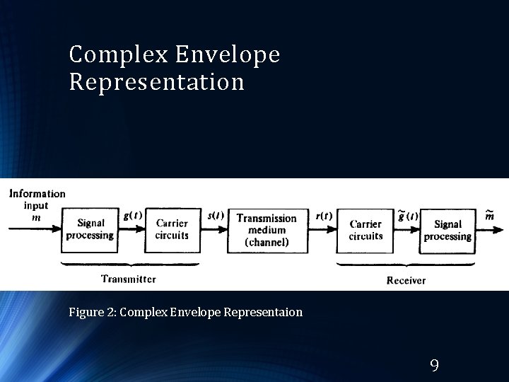
OFDM signal • g(t) is the complex envelope for OFDM signal. • fn(t) are orthogonal carriers. 7
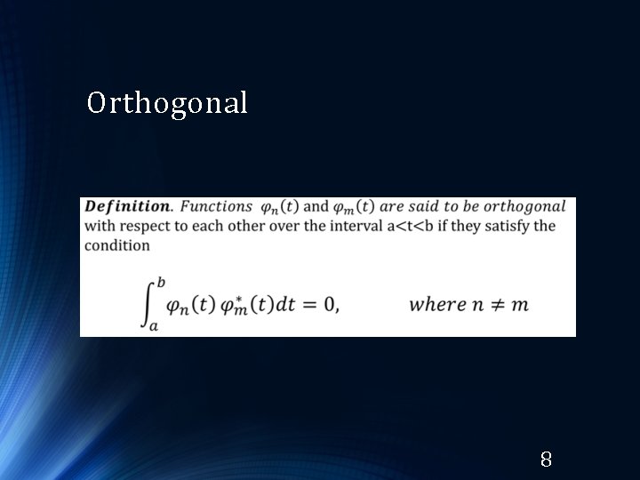
Orthogonal 8
Complex Envelope Representation Figure 2: Complex Envelope Representaion 9
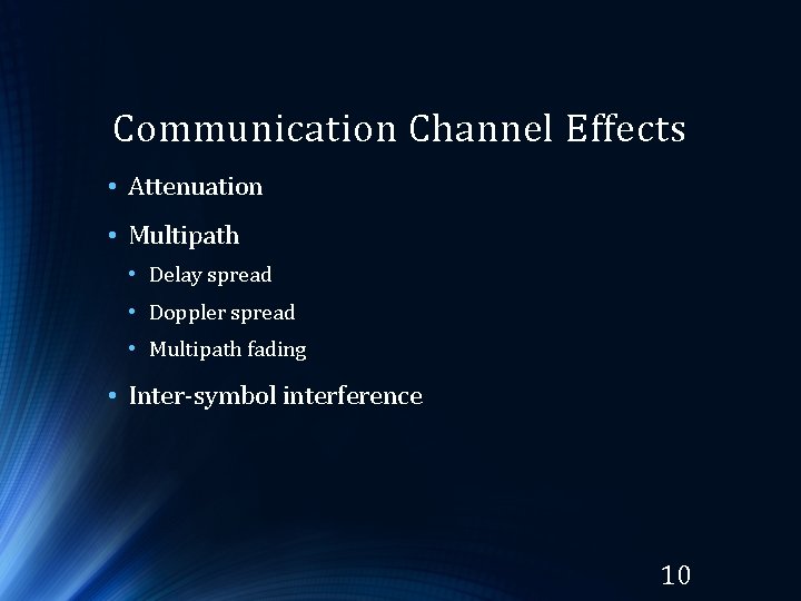
Communication Channel Effects • Attenuation • Multipath • Delay spread • Doppler spread • Multipath fading • Inter-symbol interference 10
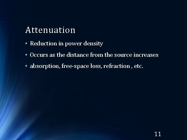
Attenuation • Reduction in power density • Occurs as the distance from the source increases • absorption, free-space loss, refraction , etc. 11
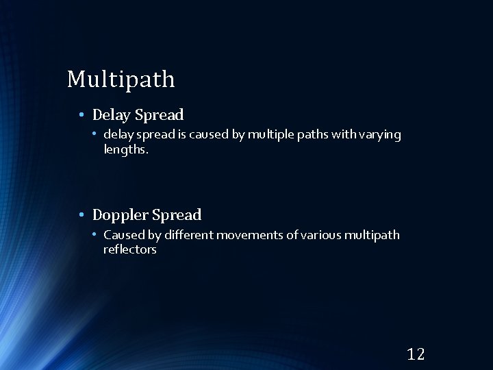
Multipath • Delay Spread • delay spread is caused by multiple paths with varying lengths. • Doppler Spread • Caused by different movements of various multipath reflectors 12
Multipath Fading • Fading caused when different multipath reflectors move around slowly and appear and disappear. • Fading is due to the received signals cancelling each other out. 13
Inter-symbol Interference (ISI) • One symbol interferes with subsequent symbols • Each symbol spreads in time, the pulse for each symbol may be smeared into adjacent symbol slots • Causes communication to be less reliable 14
Applications & Advantages • Resistant to multipath fading • Low inter-symbol interference • Widely used in digital communication systems • Used in 802. 11(a, g, n, ac), 4 G, and LTE • 4 G - 4 th generation wireless communication • LTE- Long Term Evolution 15
FFT/IFFT • This is the most important block in the OFDM communication system. • The FFT and IFFT are implemented using the Xilinx core generator. 16
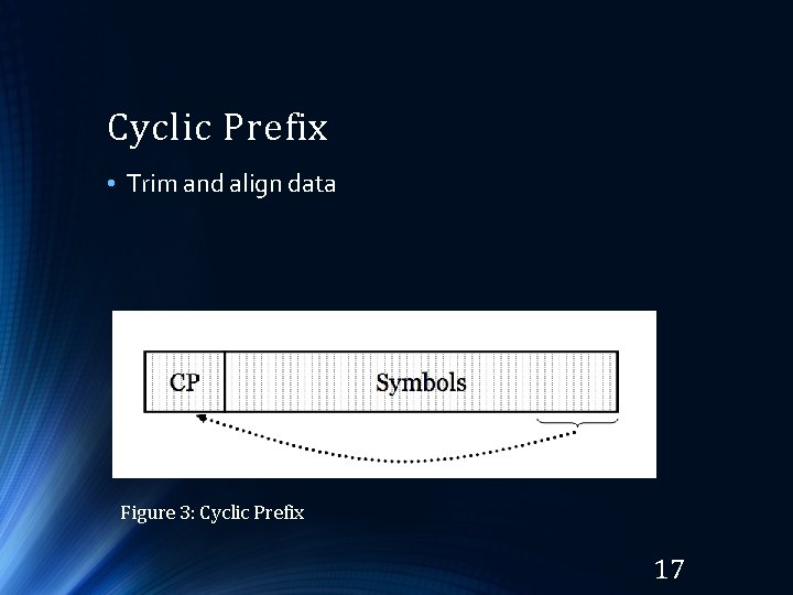
Cyclic Prefix • Trim and align data Figure 3: Cyclic Prefix 17
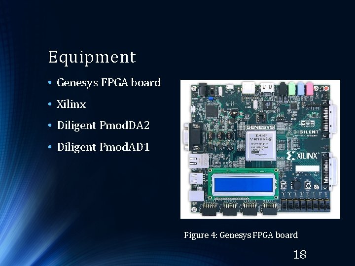
Equipment • Genesys FPGA board • Xilinx • Diligent Pmod. DA 2 • Diligent Pmod. AD 1 Figure 4: Genesys FPGA board 18
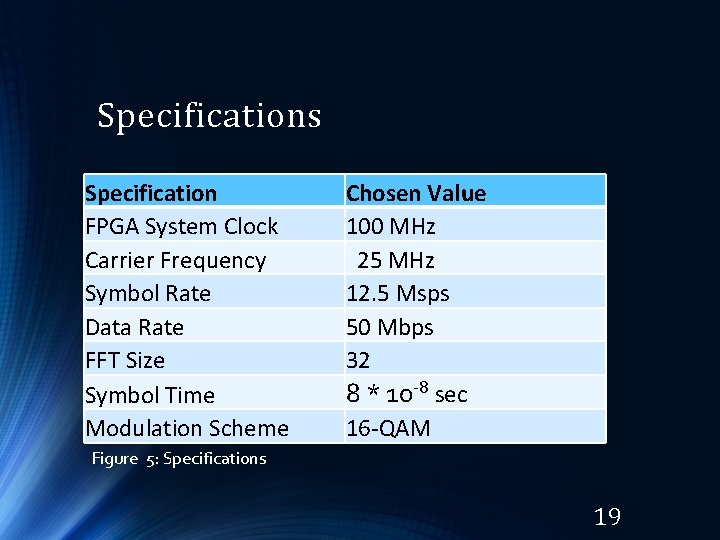
Specifications Specification FPGA System Clock Carrier Frequency Symbol Rate Data Rate FFT Size Symbol Time Modulation Scheme Chosen Value 100 MHz 25 MHz 12. 5 Msps 50 Mbps 32 8 * 10 -8 sec 16 -QAM Figure 5: Specifications 19
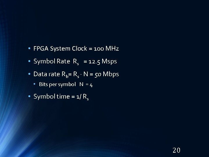
• FPGA System Clock = 100 MHz • Symbol Rate Rs = 12. 5 Msps • Data rate Rb= Rs · N = 50 Mbps • Bits per symbol N = 4 • Symbol time = 1/ Rs 20
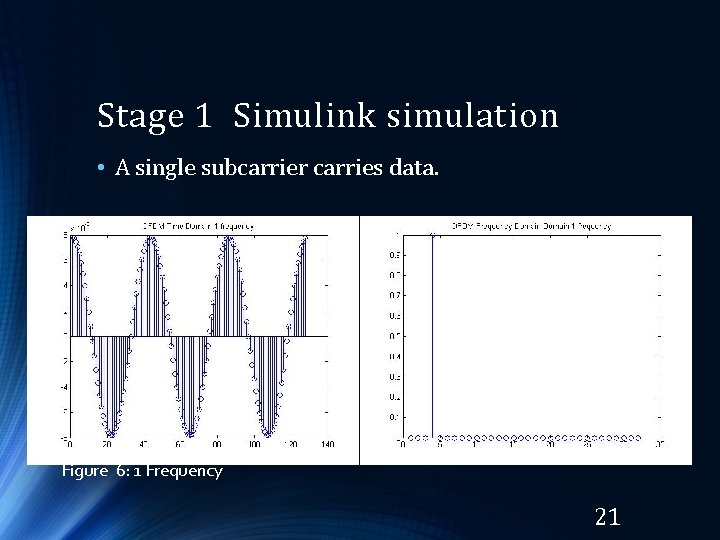
Stage 1 Simulink simulation • A single subcarrier carries data. Figure 6: 1 Frequency 21
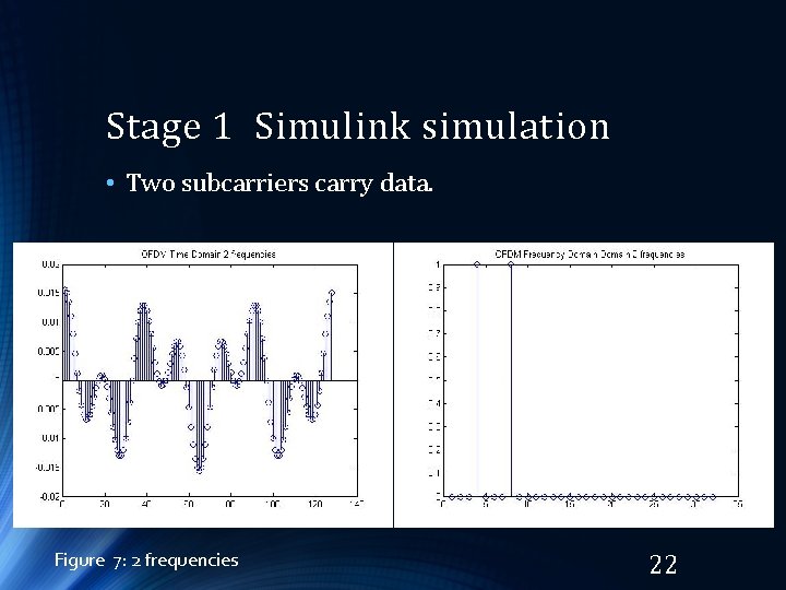
Stage 1 Simulink simulation • Two subcarriers carry data. Figure 7: 2 frequencies 22
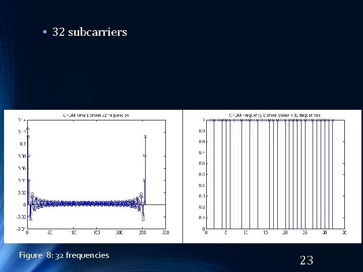
• 32 subcarriers Figure 8: 32 frequencies 23
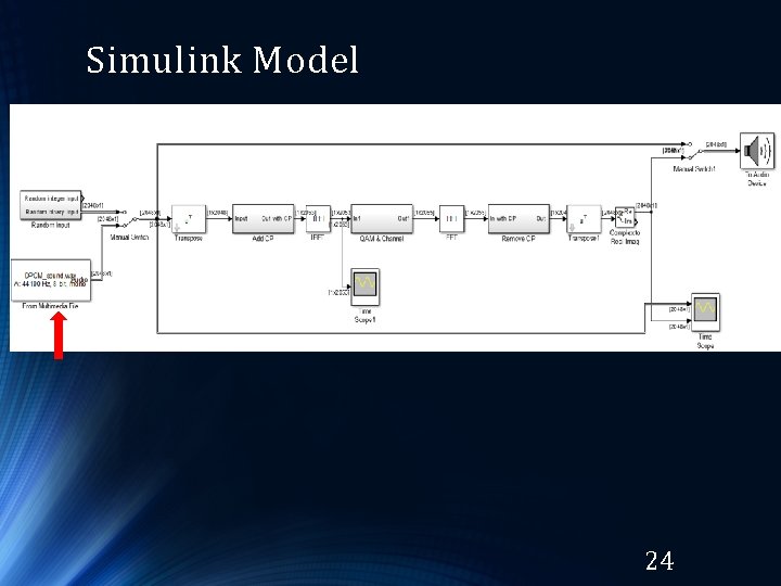
Simulink Model 24
Simulink Model 25
Simulink Model 26
Simulink Model 27
Simulink Model 28
Simulink Model 29
Simulink Model 30
Simulink Model 31
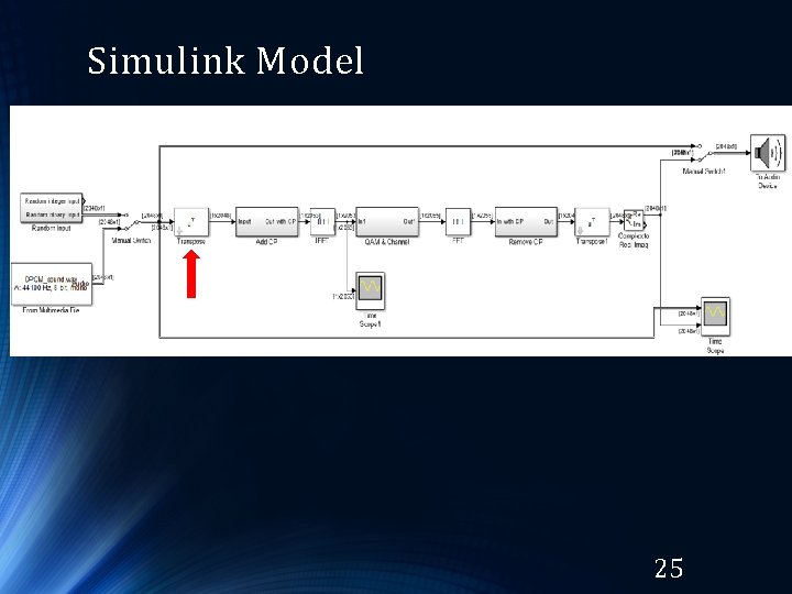
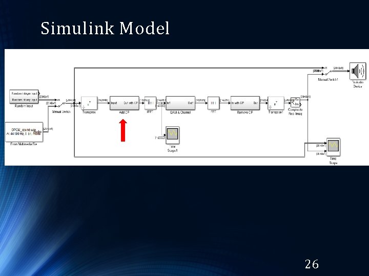
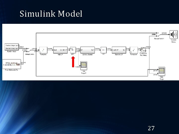
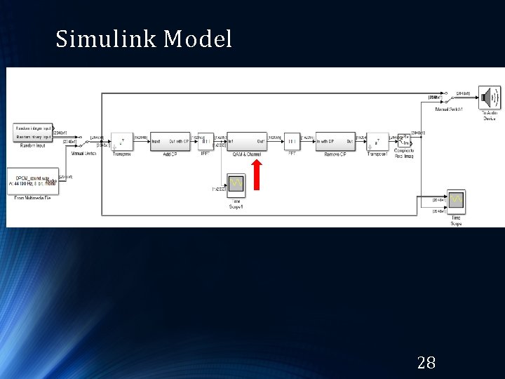
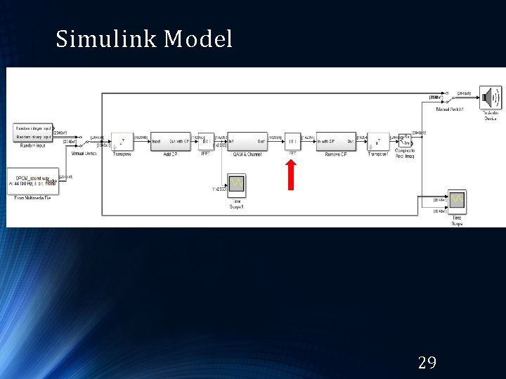
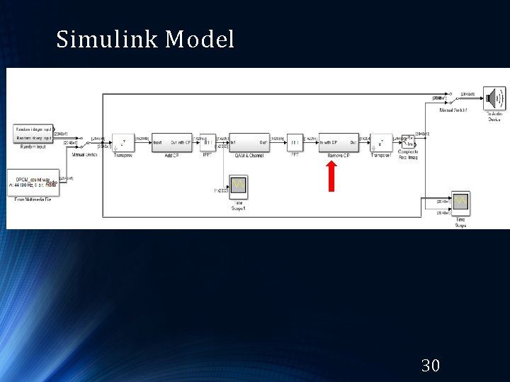
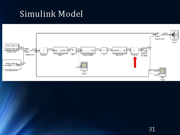
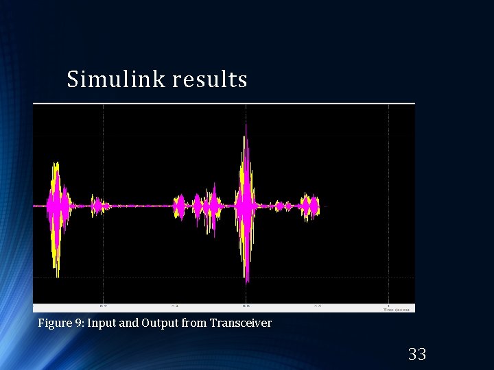
Simulink Model • Model contains transmitter, receiver, and a Gaussian channel model. • Channel model • Y(t) = x(t)*h(t) • where x(t) is the transmitted signal, h(t) is the impulse response of the channel, and y(t) is the received signal. 32
Simulink results Figure 9: Input and Output from Transceiver 33
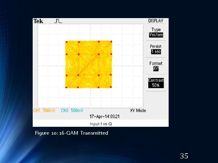
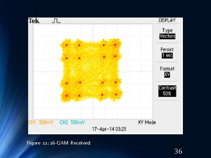
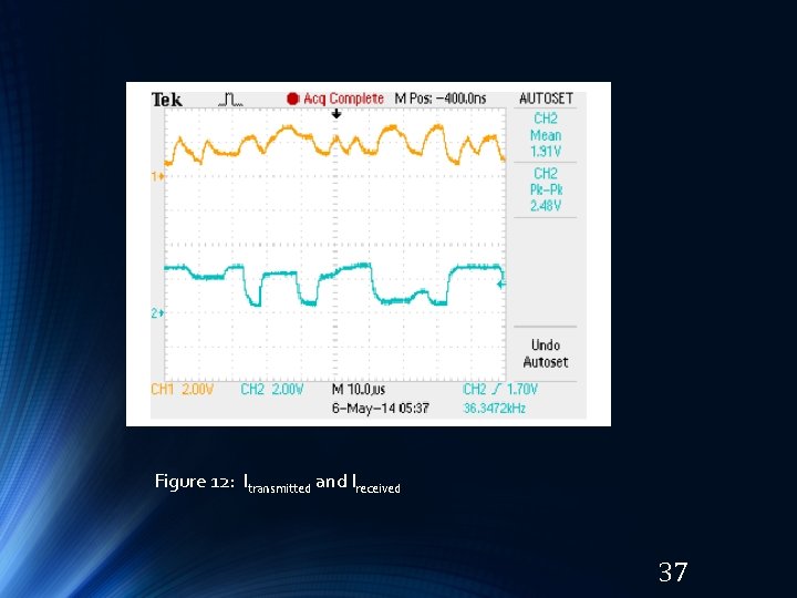
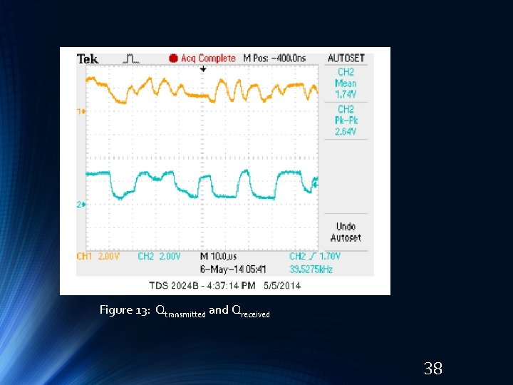
Stage 2: Implementation with channel effects • The transmitter and receiver are implemented on a FPGA board using VHDL. • Analog-to-digital converter (ADC) and digital-toanalog converter (DAC) modules are included. • Channel effects degrade the overall system performance. 34
Figure 10: 16 -QAM Transmitted 35
Figure 11: 16 -QAM Received 36
Figure 12: Itransmitted and Ireceived 37
Figure 13: Qtransmitted and Qreceived 38
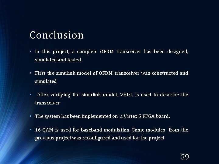
Conclusion • In this project, a complete OFDM transceiver has been designed, simulated and tested. • First the simulink model of OFDM transceiver was constructed and simulated • After verifying the simulink model, VHDL is used to describe the transceiver • The system has been implemented on a Virtex 5 FPGA board. • 16 QAM is used for baseband modulation. Some modules from the previous project was reconfigured and used for the project 39
References • [1] Anthony Gaught, Alexander Norton, and Christopher Brady. , “FPGA-based 16 QAM communication system”, Spring 2013. • [2]Leon Couch, Communication Jr. “Analog Systems”, 8 th and Digital edition, 2012, Prentice-Hall. 40
Questions 41