Advanced Digital Design with the VERILOG HDL Introduction
- Slides: 11

Advanced Digital Design with the VERILOG HDL

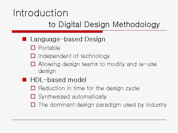
Introduction to Digital Design Methodology n Language-based Design o Portable o Independent of technology o Allowing design teams to modify and re-use design n HDL-based model o Reduction in time for the design cycle o Synthesized automatically o The dominant design paradigm used by industry

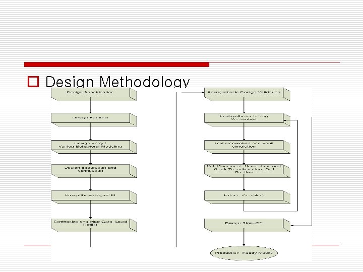
o Design Methodology

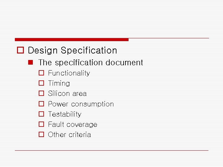
o Design Specification n The specification document o o o o Functionality Timing Silicon area Power consumption Testability Fault coverage Other criteria

o Design Partition n Configuration of interacting functional units o top-down design or hierarchical design o Design Entry n Composing a language-based description of the design and storing it in an electronic format in a computer n Behavioral modeling o Rapidly create a behavioral prototype of a design o Verify its functionality o Use a synthesis tool to optimize and map the design into a selected physical technology

o Simulation and Functional Verification n Test Plan Development n Testbench Development n Test Execution and Model Verification o Design Integration and Verification n This step in the design flow is crucial and must be executed thoroughly to ensure that the design that is being signed off for synthesis is correct

o Presynthesis Sign-Off n Sign-off occurs after all known functional errors have been eliminated o Gate-Level Synthesis and Technology Mapping n This step produces a netlist of standard cells or a database that will configure a target FPGA

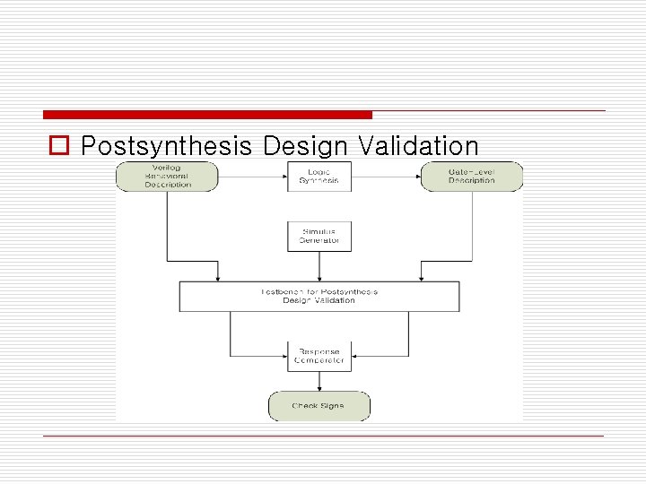
o Postsynthesis Design Validation

o Postsynthesis Timing Verification n The circuit might have to be resynthesized or re-place and rerouted to meet specifications. o Transistor resizing o Architectural modifications/substitutions o Device substitution

o Test Generation and Fault simulation n A set of test vectors n Fault simulation questions whether the chips that come off the fabrication line can be tested to verify that they operate correctly o Placement and Routing n Involve inserting a clock tree into the layout n Skew-free

o Physical and Electrical Design Rule Checks o Parasitic Extraction o Design Sign-Off n After all of the design constraints have been satisfied and timing closure has been achieved