Verilog Verilogmodule Verilog Verilog ANSI C D module

;")
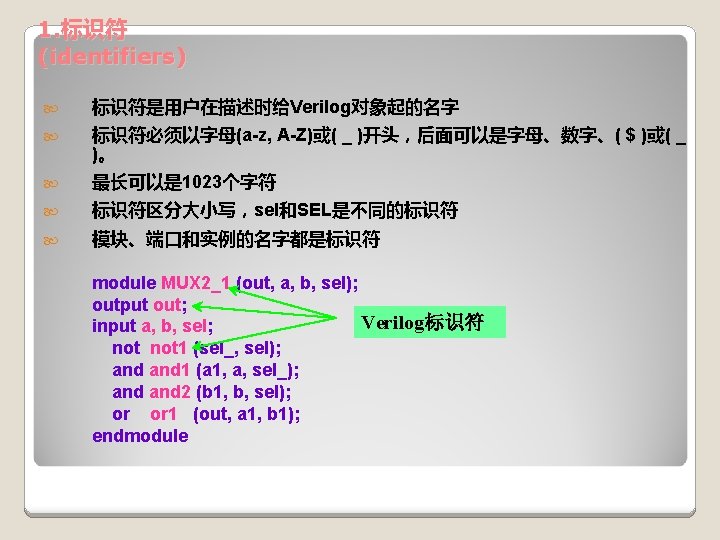
![例设计三位全加器 端口列表 模块名 sum[2: 0] module adder ( cout, sum, a, b, cin );](https://slidetodoc.com/presentation_image_h2/3e2fe7df4955c95e3a338a07f0c3cbf1/image-7.jpg "例设计三位全加器 端口列表 模块名 sum[2: 0] module adder ( cout, sum, a, b, cin );")
; output q, qb; input")
; . . endmodule REG 4( d,")
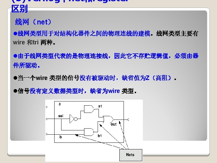
与标识符ALWAYS(非关键词)是不同的。 always and assign begin buf if")
; 格式自由 // Port declarations 单行注释")
可是整数也可以是实数 整数的大小可以定义也可以不定义。整数表示为: <size>’<base><value> 其中 size :大小,由二进制数表示的位数(bit)表示。缺省为 32位 base:数基,可为 2(b)、8(o)、10(d)、16(h)进制。缺省为 10进制 value:是所选数基内任意有效数字,包括X、Z。 实数常量可以用十进制或科学表示法表示。")
语句和门的实例的延时,但不 能用于模块的实例化。 module MUX 2_ 1 (out, a, b, sel) ; output")

![(4)Verilog中net和register声明语 法 net声明 <net_type> [range] [delay] <net_name>[, net_name]; net_type: net类型 range: 矢量范围,以[MSB:LSB]格式 delay: 定义与net相关的延时](https://slidetodoc.com/presentation_image_h2/3e2fe7df4955c95e3a338a07f0c3cbf1/image-41.jpg "(4)Verilog中net和register声明语 法 net声明 <net_type> [range] [delay] <net_name>[, net_name]; net_type: net类型 range: 矢量范围,以[MSB:LSB]格式 delay: 定义与net相关的延时")
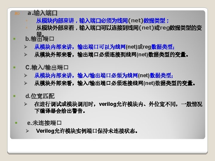
端口的数据类型选择 输入端口可以由 net/register驱动,但 输入端口只能是net 双向端口输入/输出 只能是net类型 A B 输出端口可以是 net/register类型,输 出端口只能驱动net in 1 in")
; output q, qb; input d, clk,")

![(5)寄存器数组(Register Arrays) 在Verilog中可以说明一个寄存器数组。 integer NUMS [7: 0]; // 包含 8个整数数组变量 time t_vals [3: 0];](https://slidetodoc.com/presentation_image_h2/3e2fe7df4955c95e3a338a07f0c3cbf1/image-48.jpg "(5)寄存器数组(Register Arrays) 在Verilog中可以说明一个寄存器数组。 integer NUMS [7: 0]; // 包含 8个整数数组变量 time t_vals [3: 0];")
- Slides: 49
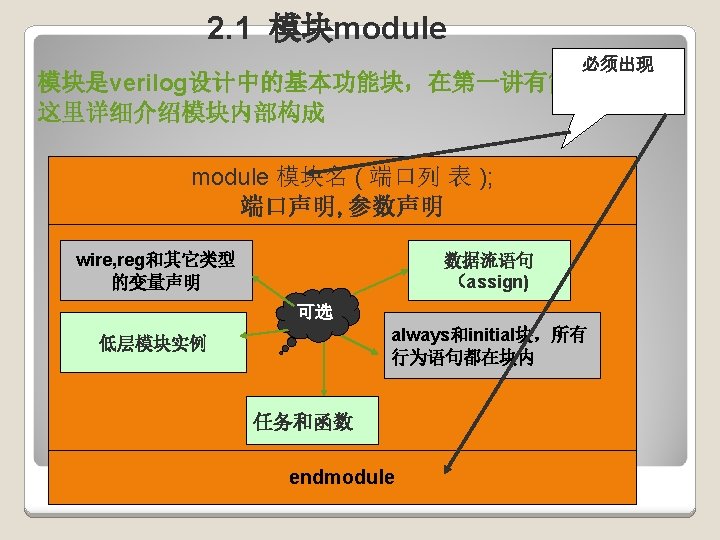
第二讲 Verilog 语法 Verilog模块module Verilog语法要素 Verilog数据类型及逻辑系统
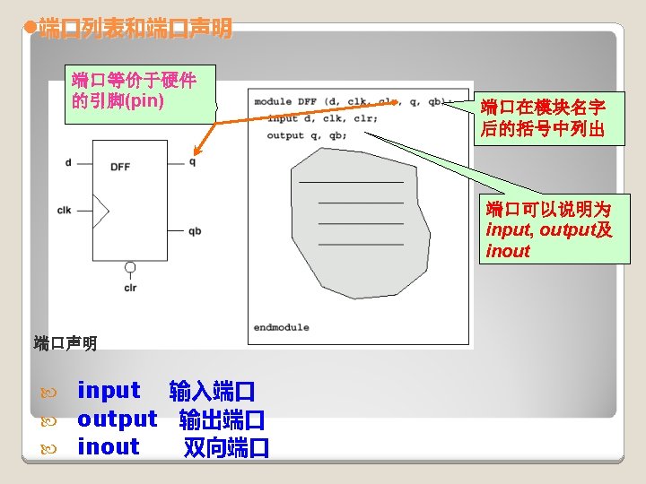
也可以采用类似ANSI C格式来声明端口 //D 触发器 module D_FF (input d, clk, clr, output reg q, qb); ………… endmodule
例设计三位全加器 端口列表 模块名 sum[2: 0] module adder ( cout, sum, a, b, cin ); cout input [2: 0] a, b; input adder cin; output cout; 端口声明 a[2: 0] b[2: 0] output [2: 0] sum; assign {cout, sum}=a+b+cin; endmodule 数据流语句 §这个例子描述了一个三位的加法器。从例子中可以看出整个 Verilog HDL程序是嵌套在module和endmodule声明语句里 的,只出现了一个assign语句。
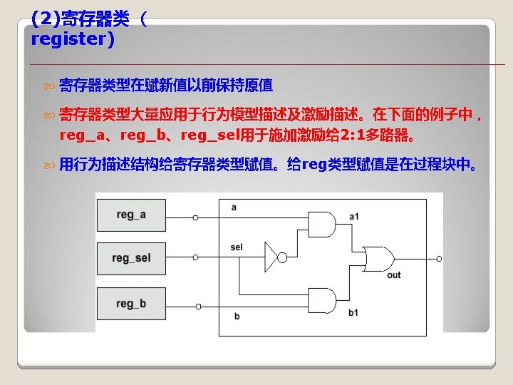
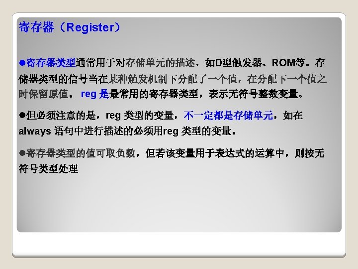
D触发器模块 //D 触发器 module D_FF (d, clk, clr, q, qb); output q, qb; input d, clk, clr; always块行为描述语句 reg q, qb; //输出端口q, qb值保存 always @(posedge clk) begin if (clr) q=1’b 0; else 该模块内包括always行为 q=d; end 块语句 not (qb, q); endmodule
4位寄存器设计 module D_FF (d, clk, clr, q, qb); . . endmodule REG 4( d, clk, clr, q, qb); output [3: 0] q, qb; input [3: 0] d; input clk, clr; D_FF d 0 (d[ 0], clk, clr, q[ 0], qb[ 0]); D_FF d 1 (d[ 1], clk, clr, q[ 1], qb[ 1]); D_FF d 2 (d[ 2], clk, clr, q[ 2], qb[ 2]); D_FF d 3 (d[ 3], clk, clr, q[ 3], qb[ 3]); endmodule 模块中只出现在低层次模块实例化
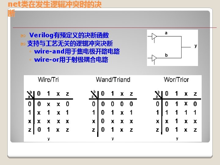
2. 关键词 Verilog HDL 定义了一系列保留字,叫做关键词。注意只有 小写的关键词才是保留字。例如,标识符always (这是个关 键词)与标识符ALWAYS(非关键词)是不同的。 always and assign begin buf if 0 bufif 1 casex casez cmos deassign default defparam disable edge else endcase endmodule endfunction endprimitive endspecify endtable endtask event force forever fork function highz 0 highz 1 if ifnone initial inout input integer join large macrmodule medium module nand negedge nmos nor notif 0 notif 1 or output parameter pmos posedge primitive pull 0 pull 1 pullup pulldown rcmos realtime reg release repeat rnmos rpmos rtranif 0 rtranif 1 scalared small specify specparam strong 0 strong 1 supply 0 supply 1 table task time tranif 0 tranif 1 tri 0 tri 1 triand trior trireg vectored wait wand weak 0 weak 1 while wire wor xnor xor
3. 空白符和注释 module MUX 2_1 (out, a, b, sel); 格式自由 // Port declarations 单行注释 使用空白符提高可读性及代码组 output out; 到行末结束 织。Verilog忽略空白符除非用于 input sel, // control input 分开其它的语言标记。 b, /* data inputs */ a; /* The netlist logic selects input ”a” when 多行注释,在/* */内 sel = 0 and it selects ”b” when sel = 1. */ not (sel_, sel); and (a 1, a, sel_), (b 1, b, sel); // What does this // line do? or (out, a 1, b 1); endmodule
4. 整数常量和实数常量 Verilog中,常量(literals)可是整数也可以是实数 整数的大小可以定义也可以不定义。整数表示为: <size>’<base><value> 其中 size :大小,由二进制数表示的位数(bit)表示。缺省为 32位 base:数基,可为 2(b)、8(o)、10(d)、16(h)进制。缺省为 10进制 value:是所选数基内任意有效数字,包括X、Z。 实数常量可以用十进制或科学表示法表示。 12 'H 83 a 8'b 1100_ 0001 64'hff 01 9'O 17 32'bz 01 x 3’b 1010_ 1101 6. 3 32 e- 4 4. 1 E 3 unsized decimal (zero-extended to 32 bits) unsized hexadecimal (zero- extended to 32 bits) 8 -bit binary 64 -bit hexadecimal (zero- extended to 64 bits) 9 -bit octal Z-extended to 32 bits 3 -bit number, truncated to 3’b 101 decimal notation scientific notation for 0. 0032 scientific notation for 4100
6. 延时说明# “#”用于说明过程(procedural)语句和门的实例的延时,但不 能用于模块的实例化。 module MUX 2_ 1 (out, a, b, sel) ; output out ; input a, b, sel ; not #1 not 1( sel_, sel); and #2 and 1( a 1, a, sel_); and #2 and 2( b 1, b, sel); or #1 or 1( out, a 1, b 1); endmodule 门延时有很多类名字:门延时(gate delay),传输延时 (propagation delay),固有延时(intrinsic delay),对象 内在延时(intra-object delay)
1. Verilog采用的四值逻辑系 统 ’ 0’, Low, False, Logic Low, Ground, VSS, Negative Assertion ‘ 1’, High, True, Logic High, Power, VDD, VCC, Positive Assertion ’X’ Unknown: Occurs at Logical Which Cannot be Resolved Conflict Hi. Z, High Impedance, Tri- Stated, Disabled Driver (Unknown)
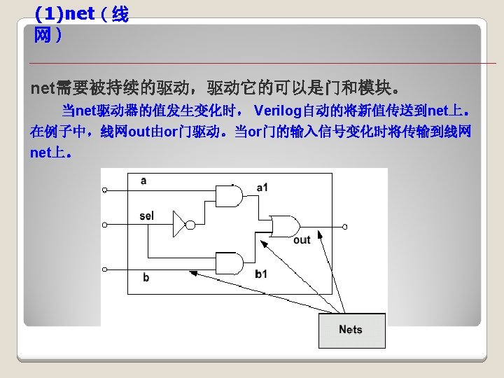
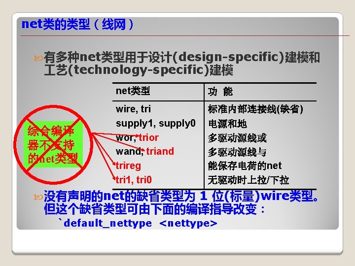
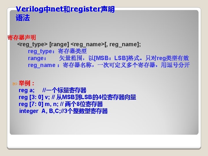
(4)Verilog中net和register声明语 法 net声明 <net_type> [range] [delay] <net_name>[, net_name]; net_type: net类型 range: 矢量范围,以[MSB:LSB]格式 delay: 定义与net相关的延时 net_name: net名称,一次可定义多个net, 用逗号分开。 § 举例: wire a; wand w; // 一个标量wand类型net tri [15: 0] busa; // 16位三态总线 wire [0: 31] w 1, w 2; // 两个 32位wire,MSB为bit 0
(5)端口的数据类型选择 输入端口可以由 net/register驱动,但 输入端口只能是net 双向端口输入/输出 只能是net类型 A B 输出端口可以是 net/register类型,输 出端口只能驱动net in 1 in 2 O Y module top; module DUT (Y, A, B); wire y; output Y; 若Y,A,B说明为 reg a, b; reg则会产生错误。 input A, B; DUT u 1 (y, a, b) ; wire Y, A, B; initial begin and (Y, A, B) ; a = 0; b = 0; endmodule #5 a = 1; end 在过程块中只能给 register类型赋值 endmodule
触发器 module D_FF (d, clk, clr, q, qb); output q, qb; input d, clk, clr; reg q, qb; //输出端口q, qb值保存 . . . endmodule //D
实例端口的互连 //D 触发器 module Top reg s 1, s 2, a, b; wire c; //调用D_FF模块,这 里命名为dff 0 D_FF dff 0 (a, b, c, s 1, s 2); ………… endmodule § § § § //D 触发器 module Top reg a, b; wire c, s 1, s 2; //调用D_FF模块,这里命 名为dff 0 D_FF dff 0 (a, b, c, s 1, s 2); ………… endmodule
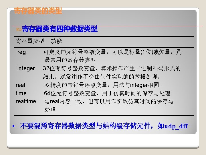
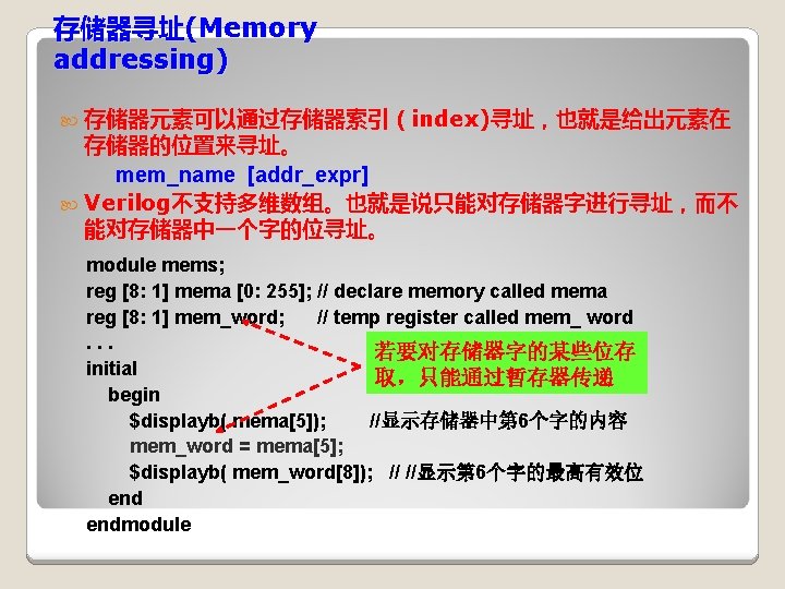
(5)寄存器数组(Register Arrays) 在Verilog中可以说明一个寄存器数组。 integer NUMS [7: 0]; // 包含 8个整数数组变量 time t_vals [3: 0]; // 4个时间数组变量 reg类型的数组通常用于描述存储器 其语法为: reg [MSB: LSB] <memory_name> <first_addr: last_addr]; [MSB: LSB]定义存储器字的位数 [first_addr: last_addr]定义存储器的深度 例如: reg [15: 0] MEM [0: 1023]; // 1 K x 16存储器 reg [7: 0] PREP [‘h. FFFE: ’h. FFFF]; // 2 x 8存储器 描述存储器时可以使用参数或任何合法表达式 parameter wordsize = 16; parameter memsize = 1024; reg [wordsize-1: 0] MEM 3 [memsize-1: 0];