Digital Design Chapter 3 Sequential Logic Design Controllers
- Slides: 49

Digital Design Chapter 3: Sequential Logic Design -- Controllers Slides to accompany the textbook Digital Design, First Edition, by Frank Vahid, John Wiley and Sons Publishers, 2007. http: //www. ddvahid. com Copyright © 2007 Frank Vahid Instructors of courses requiring Vahid's Digital Design textbook (published by John Wiley and Sons) have permission to modify and use these slides for customary course-related activities, subject to keeping this copyright notice in place and unmodified. These slides may be posted as unanimated pdf versions on publicly-accessible course websites. . Power. Point source (or pdf Digital Design with animations) may not be posted to publicly-accessible websites, but may be posted for students on internal protected sites or distributed directly to students by other electronic means. Copyright © 2006 1 Instructors may make printouts of the slides available to students for a reasonable photocopying charge, without incurring royalties. Any other use requires explicit permission. Instructors Franksource Vahid may obtain Power. Point or obtain special use permissions from Wiley – see http: //www. ddvahid. com for information.

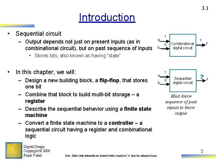
3. 1 Introduction • Sequential circuit – Output depends not just on present inputs (as in combinational circuit), but on past sequence of inputs a b 1 0 Combinational digital circuit 1 F • Stores bits, also known as having “state” • In this chapter, we will: – Design a new building block, a flip-flop, that stores one bit – Combine that block to build multi-bit storage – a register – Describe the sequential behavior using a finite state machine – Convert a finite state machine to a controller – a sequential circuit having a register and combinational logic Digital Design Copyright © 2006 Frank Vahid a b 1 0 Sequential digital circuit ? Must know sequence of past inputs to know output 2 Note: Slides with animation are denoted with a small red "a" near the animated items F

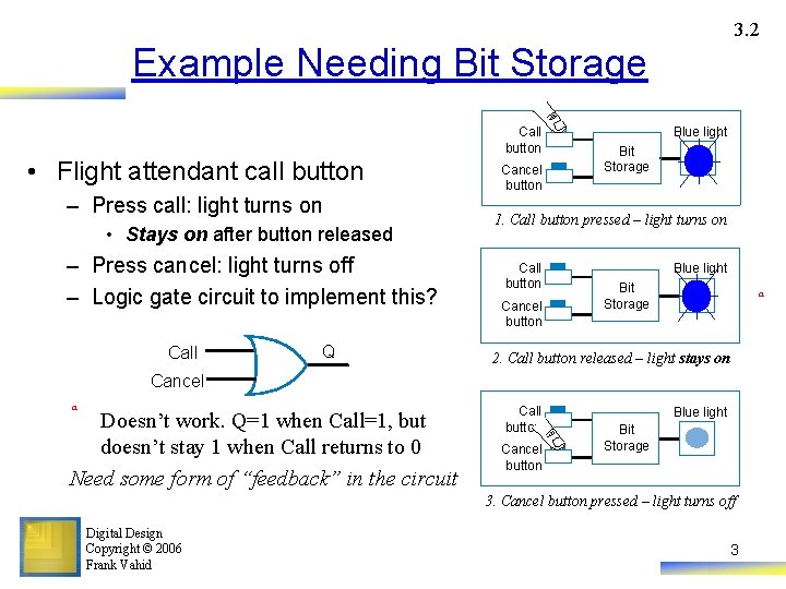
3. 2 Example Needing Bit Storage Call button • Flight attendant call button – Press call: light turns on • Stays on after button released – Press cancel: light turns off – Logic gate circuit to implement this? Call Q Cancel button Blue light Bit Storage 1. Call button pressed – light turns on Call button Cancel button Blue light Bit Storage a 2. Call button released – light stays on Cancel a Doesn’t work. Q=1 when Call=1, but doesn’t stay 1 when Call returns to 0 Need some form of “feedback” in the circuit Call button Cancel button Blue light Bit Storage 3. Cancel button pressed – light turns off Digital Design Copyright © 2006 Frank Vahid 3

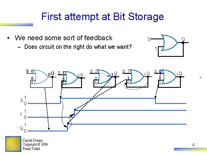
First attempt at Bit Storage • We need some sort of feedback – Does circuit on the right do what we want? S 1 0 t 1 0 Q 1 0 Digital Design Copyright © 2006 Frank Vahid 0 Q S 1 0 t 1 Q Q S S 1 1 t t 1 Q S 0 1 t 1 Q a 4

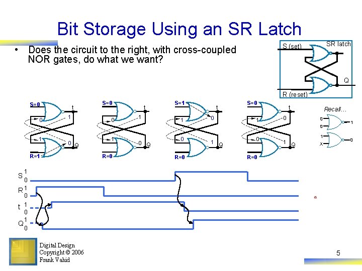
Bit Storage Using an SR Latch SR latch S (set) • Does the circuit to the right, with cross-coupled NOR gates, do what we want? Q R (reset) S=0 0 t 1 S=1 1 S=0 t 0 1 t Recall… 0 0 1 0 Q R=1 1 0 R 1 0 t 1 0 1 Q 0 1 R=0 0 Q 0 R=0 1 Q 0 1 1 0 X Q R=0 S a Digital Design Copyright © 2006 Frank Vahid 5

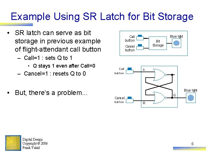
Example Using SR Latch for Bit Storage • SR latch can serve as bit storage in previous example of flight-attendant call button Blue light Call button Bit Storage Cancel button – Call=1 : sets Q to 1 • Q stays 1 even after Call=0 – Cancel=1 : resets Q to 0 • But, there’s a problem. . . Call but t on Blue light Q Cancel but t on Digital Design Copyright © 2006 Frank Vahid S R 6

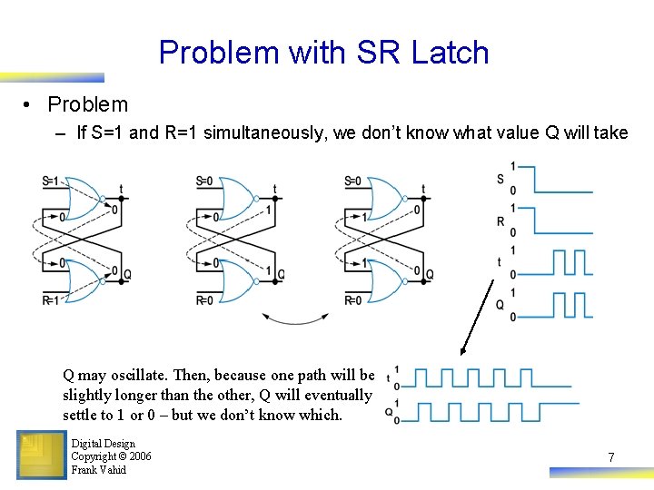
Problem with SR Latch • Problem – If S=1 and R=1 simultaneously, we don’t know what value Q will take Q may oscillate. Then, because one path will be slightly longer than the other, Q will eventually settle to 1 or 0 – but we don’t know which. Digital Design Copyright © 2006 Frank Vahid 7

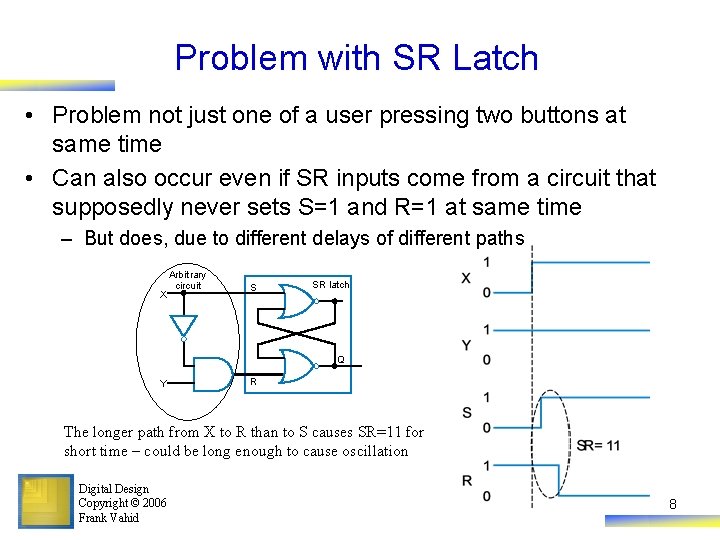
Problem with SR Latch • Problem not just one of a user pressing two buttons at same time • Can also occur even if SR inputs come from a circuit that supposedly never sets S=1 and R=1 at same time – But does, due to different delays of different paths X Arbitrary circuit S SR latch Q Y R The longer path from X to R than to S causes SR=11 for short time – could be long enough to cause oscillation Digital Design Copyright © 2006 Frank Vahid 8

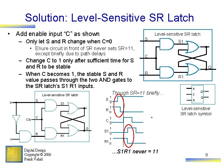
Solution: Level-Sensitive SR Latch • Add enable input “C” as shown Level-sensitive SR latch S – Only let S and R change when C=0 • Enure circuit in front of SR never sets SR=11, except briefly due to path delays – Change C to 1 only after sufficient time for S and R to be stable – When C becomes 1, the stable S and R value passes through the two AND gates to the SR latch’s S 1 R 1 inputs. Level-sensitive SR latch S X S S 1 1 S 1 C Q R R 1 Though SR=11 briefly. . . C 0 1 C 0 Q R Y R 1 S 1 C R 1 R 0 Clk S a Q’ Q Level-sensitive SR latch symbol 1 0 1 R 1 0 Digital Design Copyright © 2006 Frank Vahid . . . S 1 R 1 never = 11 9

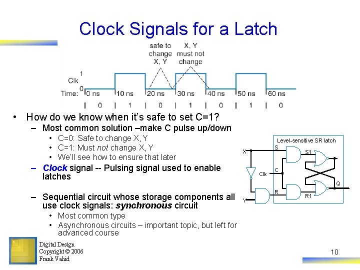
Clock Signals for a Latch • How do we know when it’s safe to set C=1? – Most common solution –make C pulse up/down • C=0: Safe to change X, Y • C=1: Must not change X, Y • We’ll see how to ensure that later X – Clock signal -- Pulsing signal used to enable latches – Sequential circuit whose storage components all use clock signals: synchronous circuit Level-sensitive SR latch S S 1 Clk C Q R Y R 1 • Most common type • Asynchronous circuits – important topic, but left for advanced course Digital Design Copyright © 2006 Frank Vahid 10

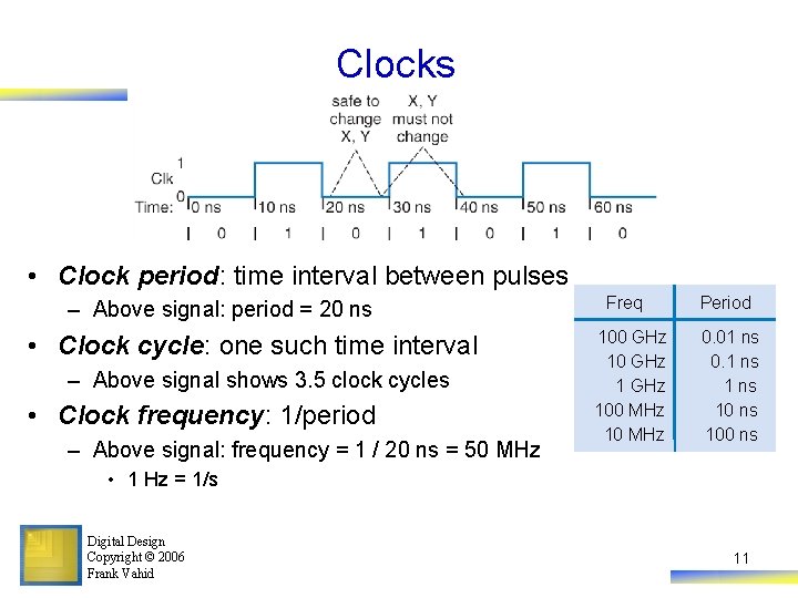
Clocks • Clock period: time interval between pulses – Above signal: period = 20 ns • Clock cycle: one such time interval – Above signal shows 3. 5 clock cycles • Clock frequency: 1/period – Above signal: frequency = 1 / 20 ns = 50 MHz Freq 100 GHz 100 MHz 10 MHz Period 0. 01 ns 0. 1 ns 100 ns • 1 Hz = 1/s Digital Design Copyright © 2006 Frank Vahid 11

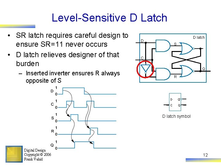
Level-Sensitive D Latch • SR latch requires careful design to ensure SR=11 never occurs • D latch relieves designer of that burden D latch D S C Q – Inserted inverter ensures R always opposite of S R D Q’ C Q D latch symbol Digital Design Copyright © 2006 Frank Vahid 12

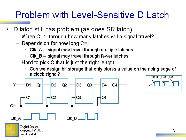
Problem with Level-Sensitive D Latch • D latch still has problem (as does SR latch) – When C=1, through how many latches will a signal travel? – Depends on for how long C=1 • Clk_A -- signal may travel through multiple latches • Clk_B -- signal may travel through fewer latches – Hard to pick C that is just the right length • Can we design bit storage that only stores a value on the rising edge of a clock signal? rising edges Clk Digital Design Copyright © 2006 Frank Vahid 13

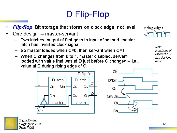
D Flip-Flop • Flip-flop: Bit storage that stores on clock edge, not level • One design -- master-servant – Two latches, output of first goes to input of second, master latch has inverted clock signal – So master loaded when C=0, then servant when C=1 – When C changes from 0 to 1, master disabled, servant loaded with value that was at D just before C changed -- i. e. , value at D during rising edge of C rising edges Clk Note: Hundreds of different flipflop designs exist D flip-flop D latch D Dm Qm Cm master D latch Ds Qs’ Cs Qs Q’ Q servant Clk Digital Design Copyright © 2006 Frank Vahid 14

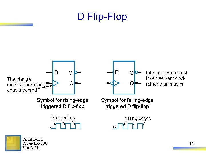
D Flip-Flop D The triangle means clock input, edge triggered Q’ D Q Symbol for rising-edge triggered D flip-flop Q Digital Design Copyright © 2006 Frank Vahid Internal design: Just invert servant clock rather than master Symbol for falling-edge triggered D flip-flop rising edges Clk Q’ falling edges Clk 15

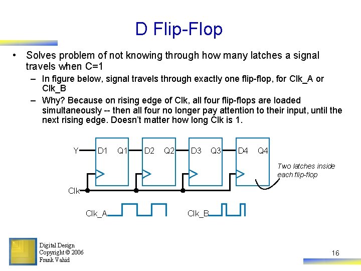
D Flip-Flop • Solves problem of not knowing through how many latches a signal travels when C=1 – In figure below, signal travels through exactly one flip-flop, for Clk_A or Clk_B – Why? Because on rising edge of Clk, all four flip-flops are loaded simultaneously -- then all four no longer pay attention to their input, until the next rising edge. Doesn’t matter how long Clk is 1. Y D 1 Q 1 D 2 Q 2 D 3 Q 3 D 4 Q 4 Two latches inside each flip-flop Clk_A Digital Design Copyright © 2006 Frank Vahid Clk_B 16

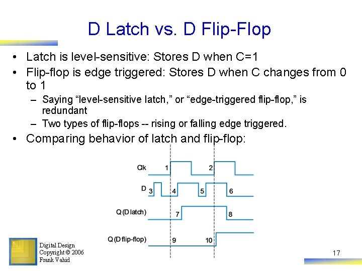
D Latch vs. D Flip-Flop • Latch is level-sensitive: Stores D when C=1 • Flip-flop is edge triggered: Stores D when C changes from 0 to 1 – Saying “level-sensitive latch, ” or “edge-triggered flip-flop, ” is redundant – Two types of flip-flops -- rising or falling edge triggered. • Comparing behavior of latch and flip-flop: Digital Design Copyright © 2006 Frank Vahid 17

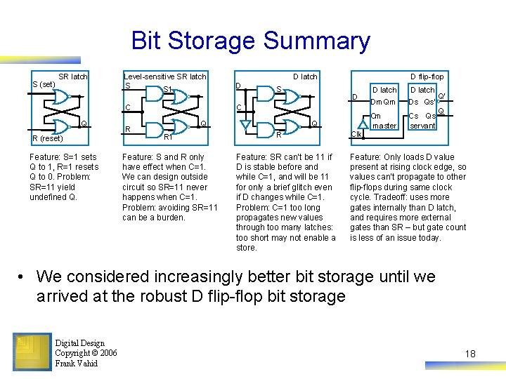
Bit Storage Summary S (set) SR latch Level-sensitive SR latch S S 1 C Q R (reset) Feature: S=1 sets Q to 1, R=1 resets Q to 0. Problem: SR=11 yield undefined Q. R D latch D S D flip-flop D C Q R 1 Feature: S and R only have effect when C=1. We can design outside circuit so SR=11 never happens when C=1. Problem: avoiding SR=11 can be a burden. Q R Feature: SR can’t be 11 if D is stable before and while C=1, and will be 11 for only a brief glitch even if D changes while C=1. Problem: C=1 too long propagates new values through too many latches: too short may not enable a store. Clk D latch Dm Qm Ds Qs’ Cm master Cs Qs servant Q’ Q Feature: Only loads D value present at rising clock edge, so values can’t propagate to other flip-flops during same clock cycle. Tradeoff: uses more gates internally than D latch, and requires more external gates than SR – but gate count is less of an issue today. • We considered increasingly better bit storage until we arrived at the robust D flip-flop bit storage Digital Design Copyright © 2006 Frank Vahid 18

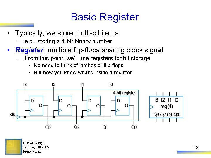
Basic Register • Typically, we store multi-bit items – e. g. , storing a 4 -bit binary number • Register: multiple flip-flops sharing clock signal – From this point, we’ll use registers for bit storage • No need to think of latches or flip-flops • But now you know what’s inside a register Digital Design Copyright © 2006 Frank Vahid 19

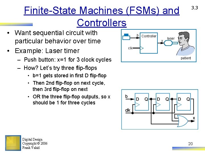
Finite-State Machines (FSMs) and Controllers • Want sequential circuit with particular behavior over time • Example: Laser timer – Push button: x=1 for 3 clock cycles – How? Let’s try three flip-flops b Controller x 3. 3 laser clk patient • b=1 gets stored in first D flip-flop • Then 2 nd flip-flop on next cycle, then 3 rd flip-flop on next • OR the three flip-flop outputs, so x should be 1 for three cycles Digital Design Copyright © 2006 Frank Vahid 20

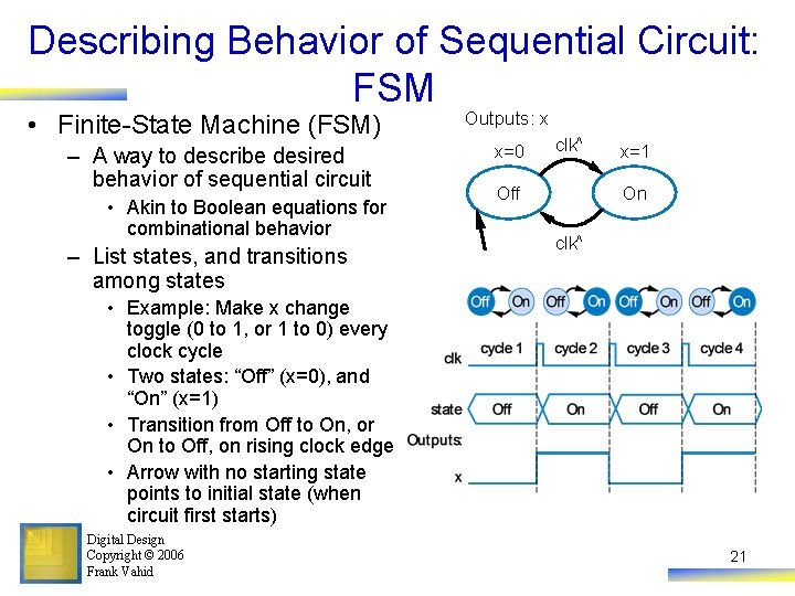
Describing Behavior of Sequential Circuit: FSM • Finite-State Machine (FSM) – A way to describe desired behavior of sequential circuit • Akin to Boolean equations for combinational behavior – List states, and transitions among states Outputs: x x=0 clk^ Off x=1 On clk^ • Example: Make x change toggle (0 to 1, or 1 to 0) every clock cycle • Two states: “Off” (x=0), and “On” (x=1) • Transition from Off to On, or On to Off, on rising clock edge • Arrow with no starting state points to initial state (when circuit first starts) Digital Design Copyright © 2006 Frank Vahid 21

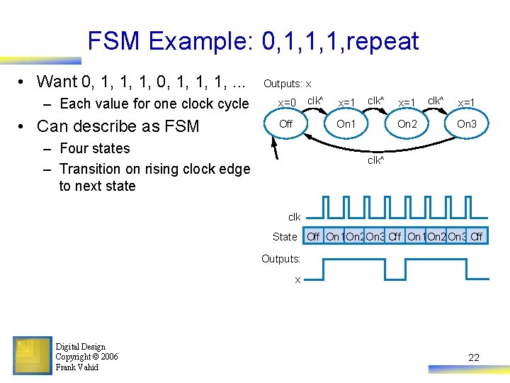
FSM Example: 0, 1, 1, 1, repeat • Want 0, 1, 1, 1, . . . – Each value for one clock cycle • Can describe as FSM Outputs: x x=0 Off clk^ x=1 clk^ On 1 – Four states – Transition on rising clock edge to next state x=1 On 2 clk^ x=1 On 3 clk^ clk State Off On 1 On 2 On 3 Off On 1 On 2 On 3 Off Outputs: x Digital Design Copyright © 2006 Frank Vahid 22

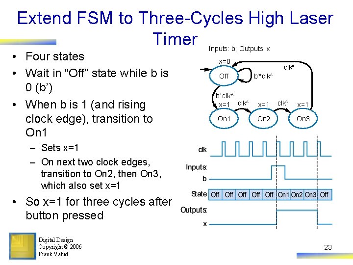
Extend FSM to Three-Cycles High Laser Timer • Four states • Wait in “Off” state while b is 0 (b’) • When b is 1 (and rising clock edge), transition to On 1 Inputs: b; Outputs: x x=0 Off clk^ b’*clk^ b*clk^ x=1 On 2 clk^ x=1 On 3 – Sets x=1 – On next two clock edges, transition to On 2, then On 3, which also set x=1 • So x=1 for three cycles after button pressed Digital Design Copyright © 2006 Frank Vahid 23

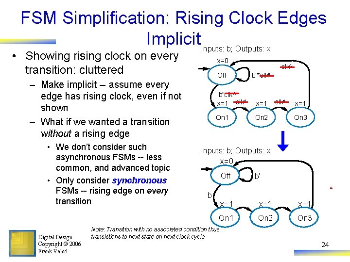
FSM Simplification: Rising Clock Edges Implicit. Inputs: b; Outputs: x • Showing rising clock on every transition: cluttered x=0 Off – Make implicit -- assume every edge has rising clock, even if not shown – What if we wanted a transition without a rising edge • We don’t consider such asynchronous FSMs -- less common, and advanced topic • Only consider synchronous FSMs -- rising edge on every transition Digital Design Copyright © 2006 Frank Vahid clk^ b’ *clk^ b*clk ^ x=1 clk^ x=1 On 2 clk^ x=1 On 3 Inputs: b; Outputs: x x=0 Off b’ a b x=1 x=1 On 2 On 3 Note: Transition with no associated condition thus transistions to next state on next clock cycle 24

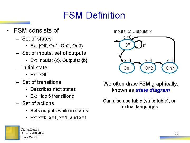
FSM Definition • FSM consists of – Set of states Inputs: b; Outputs: x x=0 Off • Ex: {Off, On 1, On 2, On 3} – Set of inputs, set of outputs • Ex: Inputs: {x}, Outputs: {b} – Initial state b’ b x=1 x=1 On 2 On 3 • Ex: “Off” – Set of transitions • Describes next states • Ex: Has 5 transitions – Set of actions • Sets outputs while in states • Ex: x=0, x=1, and x=1 Digital Design Copyright © 2006 Frank Vahid We often draw FSM graphically, known as state diagram Can also use table (state table), or textual languages 25

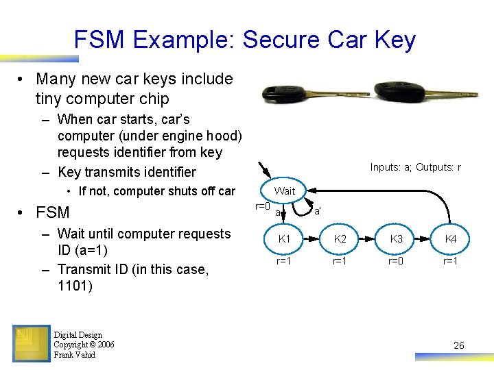
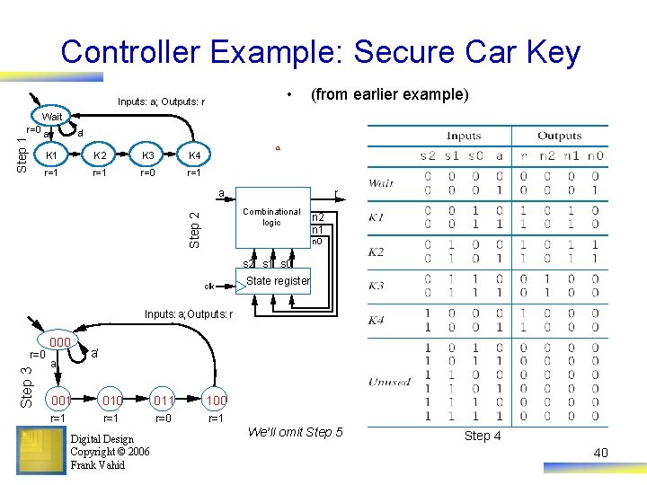
FSM Example: Secure Car Key • Many new car keys include tiny computer chip – When car starts, car’s computer (under engine hood) requests identifier from key – Key transmits identifier Inputs: a; Outputs: r • If not, computer shuts off car • FSM – Wait until computer requests ID (a=1) – Transmit ID (in this case, 1101) Digital Design Copyright © 2006 Frank Vahid Wait r=0 a a’ K 1 K 2 K 3 K 4 r=1 r=0 r=1 26

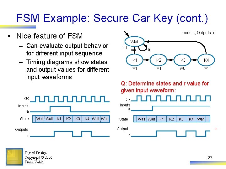
FSM Example: Secure Car Key (cont. ) Inputs: a; Outputs: r • Nice feature of FSM – Can evaluate output behavior for different input sequence – Timing diagrams show states and output values for different input waveforms clk r=0 a a’ K 1 K 2 K 3 K 4 r=1 r=0 r=1 Q: Determine states and r value for given input waveform: clk Inputs a State Wait Outputs r Digital Design Copyright © 2006 Frank Vahid K 1 K 2 K 3 K 4 Wait State Wait K 1 K 2 K 3 K 4 Wait K 1 Output a r 27

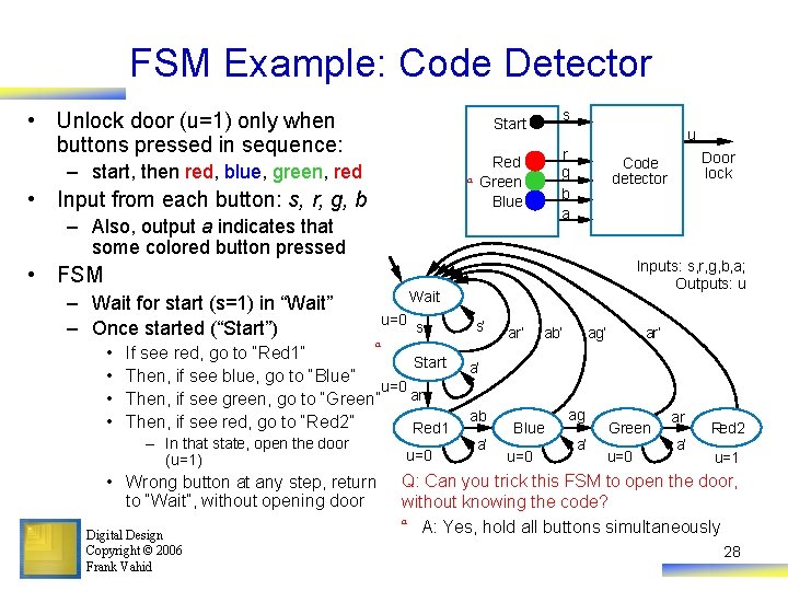
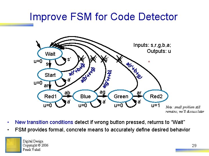
FSM Example: Code Detector • Unlock door (u=1) only when buttons pressed in sequence: s Start – start, then red, blue, green, red u r g b a Red Green Blue a • Input from each button: s, r, g, b – Also, output a indicates that some colored button pressed Inputs: s, r, g, b, a; Outputs: u • FSM – Wait for start (s=1) in “Wait” – Once started (“Start”) • • Wait u=0 s – In that state, open the door (u=1) • Wrong button at any step, return to “Wait”, without opening door Digital Design Copyright © 2006 Frank Vahid s’ a If see red, go to “Red 1” Start Then, if see blue, go to “Blue” u=0 ar Then, if see green, go to “Green” Then, if see red, go to “Red 2” Red 1 u=0 Door lock Code detector ar’ ab’ ag’ ar’ a’ ab a’ Blue u=0 ag a’ Green u=0 ar a’ Red 2 u=1 Q: Can you trick this FSM to open the door, without knowing the code? a A: Yes, hold all buttons simultaneously 28

Improve FSM for Code Detector Wait u=0 s Start u=0 ar Red 1 u=0 • • Inputs: s, r, g, b, a; Outputs: u s’ ar’ ab’ ag’ ar’ a a’ ab a’ Blue u=0 ag a’ Green u=0 ar a’ Red 2 u=1 Note: small problem still remains; we’ll discuss later New transition conditions detect if wrong button pressed, returns to “Wait” FSM provides formal, concrete means to accurately define desired behavior Digital Design Copyright © 2006 Frank Vahid 29

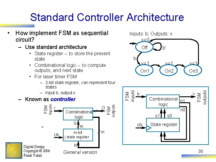
Standard Controller Architecture Inputs: b; Outputs: x x=0 – Use standard architecture Off – 2 -bit state register, can represent four states – Input b, output x I S a clk Digital Design Copyright © 2006 Frank Vahid Combinational logic O x=1 On 2 On 3 x b Combinational n 1 logic n 0 s 1 s 0 clk m m-bit state register x=1 FSM outputs FSM inputs – Known as controller b FSM inputs • State register -- to store the present state • Combinational logic -- to compute outputs, and next state • For laser timer FSM b’ FSM outputs • How implement FSM as sequential circuit? State register m N General version 30

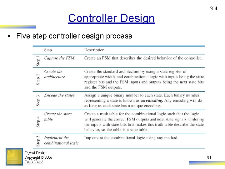
3. 4 Controller Design • Five step controller design process Digital Design Copyright © 2006 Frank Vahid 31

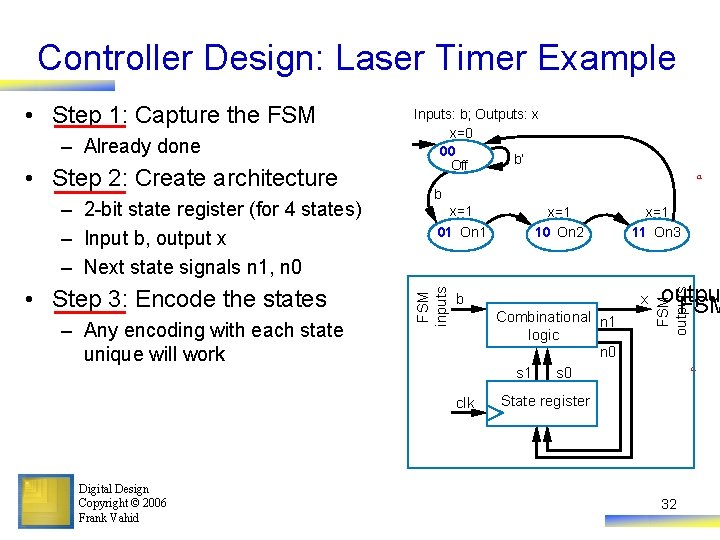
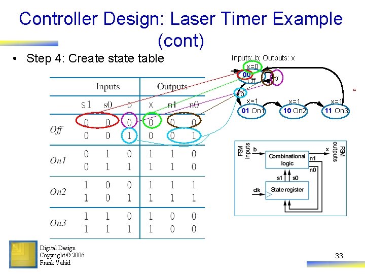
Controller Design: Laser Timer Example • Step 2: Create architecture – 2 -bit state register (for 4 states) – Input b, output x – Next state signals n 1, n 0 • Step 3: Encode the states – Any encoding with each state unique will work b x=1 01 On 1 x=1 10 On 2 x=1 11 On 3 x b Combinational n 1 logic n 0 s 1 s 0 clk Digital Design Copyright © 2006 Frank Vahid a outpu FSM outputs – Already done Inputs: b; Outputs: x x=0 00 b’ Off FSM inputs • Step 1: Capture the FSM a State register 32

Controller Design: Laser Timer Example (cont) • Step 4: Create state table Inputs: b; Outputs: x x=0 00 b’ Off b x=1 01 On 1 Digital Design Copyright © 2006 Frank Vahid a x=1 10 On 2 x=1 11 On 3 33

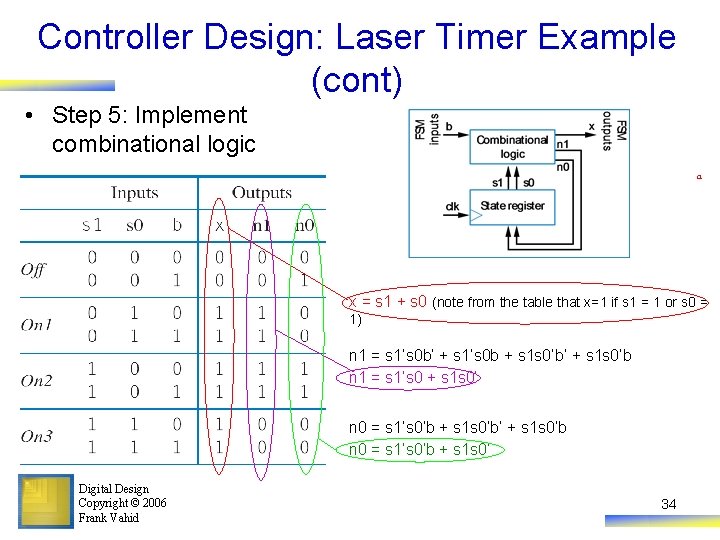
Controller Design: Laser Timer Example (cont) • Step 5: Implement combinational logic a x = s 1 + s 0 (note from the table that x=1 if s 1 = 1 or s 0 = 1) n 1 = s 1’s 0 b’ + s 1’s 0 b + s 1 s 0’b’ + s 1 s 0’b n 1 = s 1’s 0 + s 1 s 0’ n 0 = s 1’s 0’b + s 1 s 0’b’ + s 1 s 0’b n 0 = s 1’s 0’b + s 1 s 0’ Digital Design Copyright © 2006 Frank Vahid 34

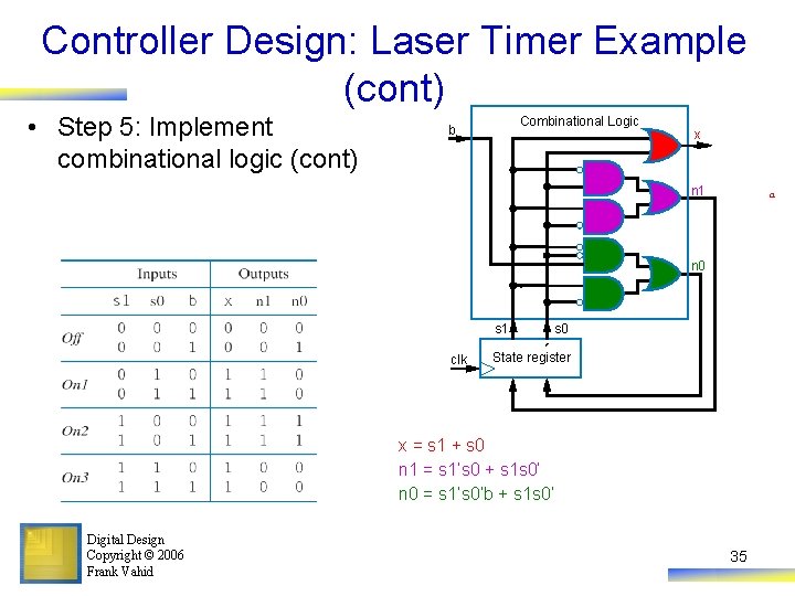
Controller Design: Laser Timer Example (cont) • Step 5: Implement combinational logic (cont) Combinational Logic b x n 1 a n 0 s 1 clk s 0 State register x = s 1 + s 0 n 1 = s 1’s 0 + s 1 s 0’ n 0 = s 1’s 0’b + s 1 s 0’ Digital Design Copyright © 2006 Frank Vahid 35

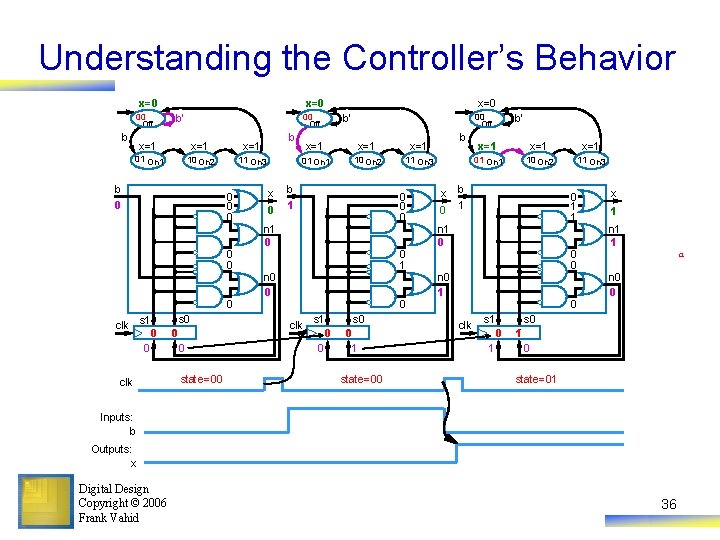
Understanding the Controller’s Behavior x=0 00 Off b b’ b x=1 x=1 01 On 1 10 On 2 11 On 3 b 0 0 0 0 clk s 1 0 0 clk x=0 00 Off s 0 0 0 state=00 x 0 00 Off b’ x=1 x=1 01 On 1 10 On 2 11 On 3 b 1 0 0 0 n 1 0 0 1 n 0 0 0 clk s 1 0 0 s 0 0 1 state=00 b x 0 b’ x=1 x=1 01 On 1 10 On 2 11 On 3 b 1 0 1 1 n 1 0 0 0 n 0 1 0 clk s 1 1 n 1 1 a n 0 0 s 0 0 1 x 1 0 state=01 Inputs: b Outputs: x Digital Design Copyright © 2006 Frank Vahid 36

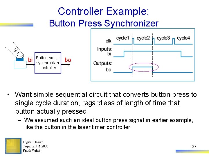
Controller Example: Button Press Synchronizer bi Button press synchronizer controller bo • Want simple sequential circuit that converts button press to single cycle duration, regardless of length of time that button actually pressed – We assumed such an ideal button press signal in earlier example, like the button in the laser timer controller Digital Design Copyright © 2006 Frank Vahid 37

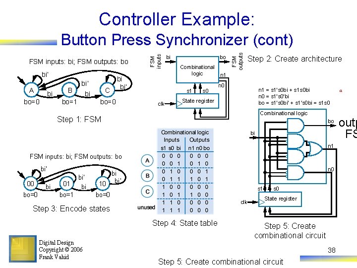
Controller Example: bi’ A bi bo=0 B bi C bi’ bi bo=1 bo=0 bi bo Combinational logic s 1 clk s 0 FSM outputs FSM inputs: bi; FSM outputs: bo FSM inputs Button Press Synchronizer (cont) Step 2: Create architecture n 1 n 0 n 1 = s 1’s 0 bi + s 1 s 0 bi n 0 = s 1’s 0’bi bo = s 1’s 0 bi’ + s 1’s 0 bi = s 1 s 0 State register Combinational logic Step 1: FSM bo bi n 1 FSM inputs: bi; FSM outputs: bo bi’ 00 bo=0 bi 01 bi’ bi bo=1 n 0 bi 10 bi’ s 1 bo=0 clk Step 3: Encode states Step 4: State table Digital Design Copyright © 2006 Frank Vahid s 0 State register Step 5: Create combinational circuit 38 Step 5: Create combinational circuit a outp FS

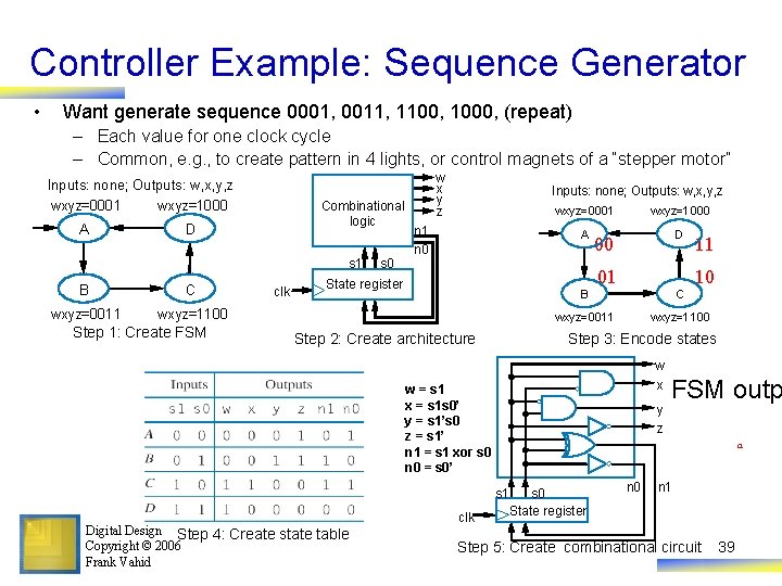
Controller Example: Sequence Generator • Want generate sequence 0001, 0011, 1100, 1000, (repeat) – Each value for one clock cycle – Common, e. g. , to create pattern in 4 lights, or control magnets of a “stepper motor” w x y z Inputs: none; Outputs: w, x, y, z wxyz=0001 wxyz=1000 A D Combinational logic s 1 B C wxyz=0011 wxyz=1100 Step 1: Create FSM clk s 0 Inputs: none; Outputs: w, x, y, z n 1 n 0 State register wxyz=0001 wxyz=1000 A D B 00 01 C wxyz=0011 Step 2: Create architecture Step 3: Encode states w x y z FSM outp a s 1 clk 10 wxyz=1100 w = s 1 x = s 1 s 0’ y = s 1’s 0 z = s 1’ n 1 = s 1 xor s 0 n 0 = s 0’ Digital Design Step 4: Create state table Copyright © 2006 Frank Vahid 11 s 0 State register n 0 n 1 Step 5: Create combinational circuit 39

Controller Example: Secure Car Key • Inputs: a; Outputs: r Step 1 Wait r=0 a (from earlier example) a’ K 1 K 2 K 3 K 4 r=1 r=0 r=1 a a r Step 2 Combinational logic n 2 n 1 n 0 s 2 s 1 s 0 clk State register Inputs: a; Outputs: r Step 3 r=0 000 a’ a 001 010 011 100 r=1 r=0 r=1 Digital Design Copyright © 2006 Frank Vahid We’ll omit Step 5 Step 4 40

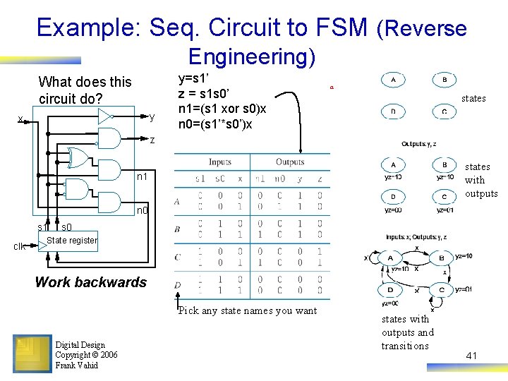
Example: Seq. Circuit to FSM (Reverse Engineering) What does this circuit do? y x y=s 1’ z = s 1 s 0’ n 1=(s 1 xor s 0)x n 0=(s 1’*s 0’)x a states z states with outputs n 1 n 0 s 1 clk s 0 State register Work backwards Pick any state names you want Digital Design Copyright © 2006 Frank Vahid states with outputs and transitions 41

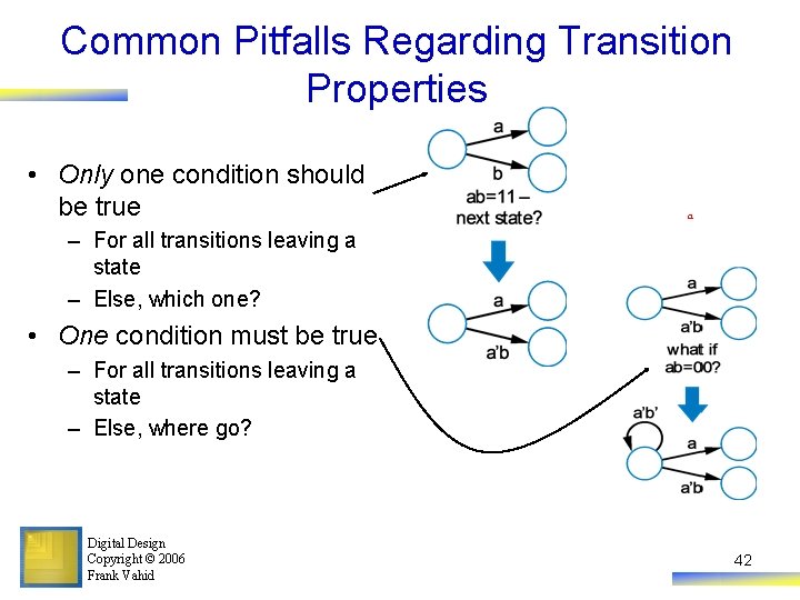
Common Pitfalls Regarding Transition Properties • Only one condition should be true a – For all transitions leaving a state – Else, which one? • One condition must be true – For all transitions leaving a state – Else, where go? Digital Design Copyright © 2006 Frank Vahid 42

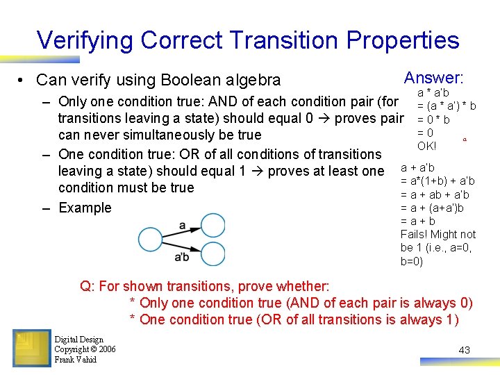
Verifying Correct Transition Properties • Can verify using Boolean algebra Answer: a * a’b = (a * a’) * b =0*b =0 a OK! – Only one condition true: AND of each condition pair (for transitions leaving a state) should equal 0 proves pair can never simultaneously be true – One condition true: OR of all conditions of transitions leaving a state) should equal 1 proves at least one a + a’b = a*(1+b) + a’b condition must be true = a + ab + a’b = a + (a+a’)b – Example =a+b Fails! Might not be 1 (i. e. , a=0, b=0) Q: For shown transitions, prove whether: * Only one condition true (AND of each pair is always 0) * One condition true (OR of all transitions is always 1) Digital Design Copyright © 2006 Frank Vahid 43

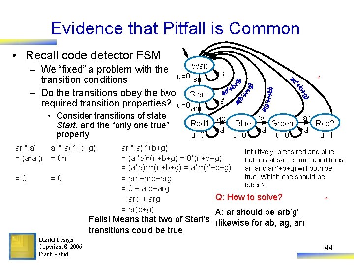
Evidence that Pitfall is Common • Recall code detector FSM Wait – We “fixed” a problem with the u=0 s transition conditions – Do the transitions obey the two Start required transition properties? u=0 ar • Consider transitions of state Start, and the “only one true” property ar * a’ a’ * a(r’+b+g) = (a*a’)r = 0*r =0 =0 Red 1 u=0 s’ a a’ ab a’ Blue u=0 ag a’ Green u=0 ar a’ Red 2 u=1 ar * a(r’+b+g) Intuitively: press red and blue = (a’*a)*(r’+b+g) = 0*(r’+b+g) buttons at same time: conditions = (a*a)*r*(r’+b+g) = a*r*(r’+b+g) ar, and a(r’+b+g) will both be true. Which one should be = arr’+arb+arg taken? = 0 + arb+arg a Q: How to solve? = arb + arg = ar(b+g) A: ar should be arb’g’ Fails! Means that two of Start’s (likewise for ab, ag, ar) transitions could be true Digital Design Copyright © 2006 Frank Vahid 44

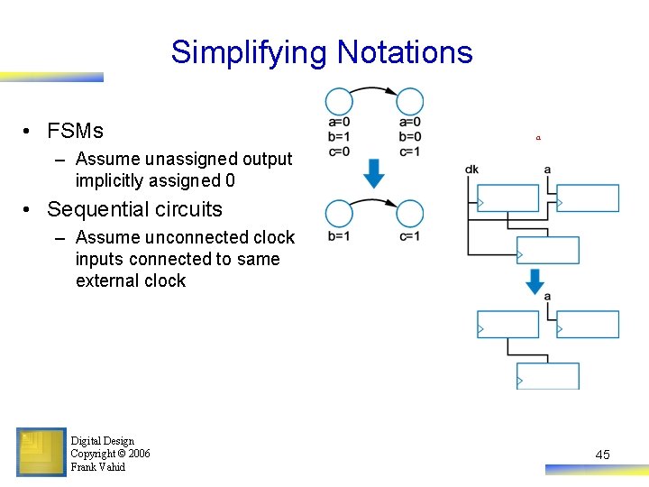
Simplifying Notations • FSMs a – Assume unassigned output implicitly assigned 0 • Sequential circuits – Assume unconnected clock inputs connected to same external clock Digital Design Copyright © 2006 Frank Vahid 45

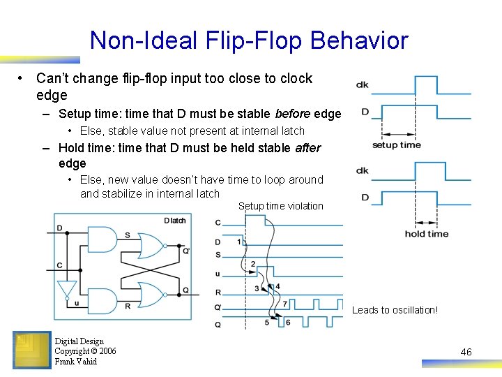
Non-Ideal Flip-Flop Behavior • Can’t change flip-flop input too close to clock edge – Setup time: time that D must be stable before edge • Else, stable value not present at internal latch – Hold time: time that D must be held stable after edge • Else, new value doesn’t have time to loop around and stabilize in internal latch Setup time violation Leads to oscillation! Digital Design Copyright © 2006 Frank Vahid 46

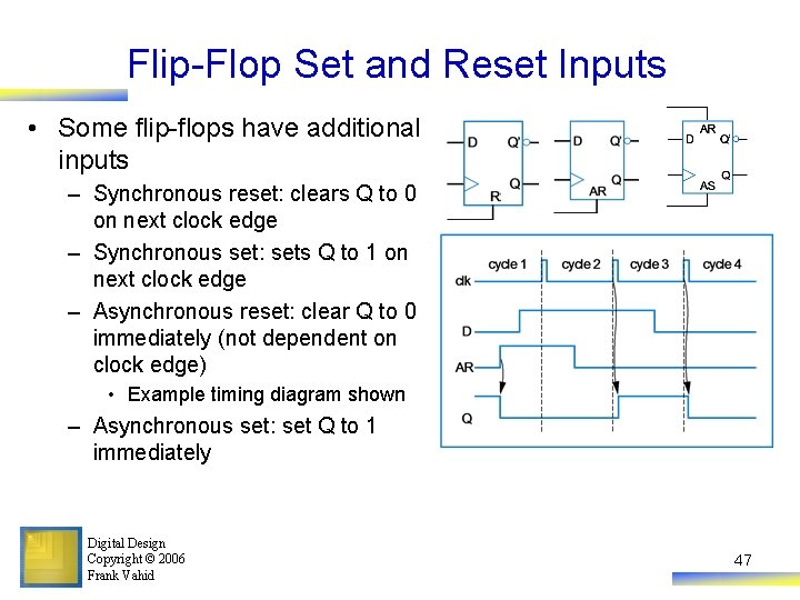
Flip-Flop Set and Reset Inputs • Some flip-flops have additional inputs – Synchronous reset: clears Q to 0 on next clock edge – Synchronous set: sets Q to 1 on next clock edge – Asynchronous reset: clear Q to 0 immediately (not dependent on clock edge) • Example timing diagram shown – Asynchronous set: set Q to 1 immediately Digital Design Copyright © 2006 Frank Vahid 47

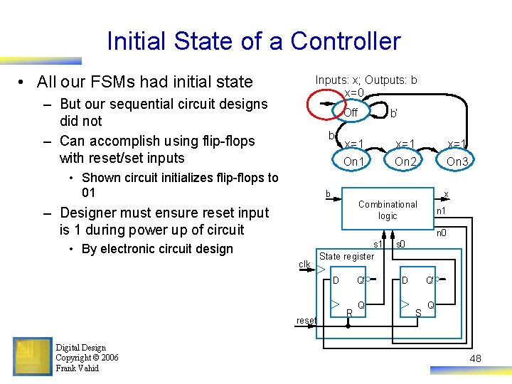
Initial State of a Controller • All our FSMs had initial state Inputs: x; Outputs: b x=0 – But our sequential circuit designs did not – Can accomplish using flip-flops with reset/set inputs Off b • Shown circuit initializes flip-flops to 01 x=1 x=1 On 2 On 3 b x Combinational logic – Designer must ensure reset input is 1 during power up of circuit n 1 n 0 • By electronic circuit design clk s 1 State register D reset Digital Design Copyright © 2006 Frank Vahid b’ Q’ R Q s 0 D Q’ S Q 48

Chapter Summary • Sequential circuits – Have state • Created robust bit-storage device: D flip-flop – Put several together to build register, which we used to hold state • Defined FSM formal model to describe sequential behavior – Using solid mathematical models -- Boolean equations for combinational circuit, and FSMs for sequential circuits -- is very important. • Defined 5 -step process to convert FSM to sequential circuit – Controller • So now we know how to build the class of sequential circuits known as controllers Digital Design Copyright © 2006 Frank Vahid 49