Digital Design and System Implementation z Overview of

- Slides: 32
Digital Design and System Implementation z Overview of Physical Implementations z CMOS devices z CMOS transistor circuit functional behavior y Basic logic gates y Transmission gates y Tri-state buffers y Flip-flops vs. latches revisited CS 150 – Spring 2007 - Lec #26 – Digital Design – 1
Overview of Physical Implementations The stuff out of which we make systems z Integrated Circuits (ICs) y Combinational logic circuits, memory elements, analog interfaces z Printed Circuits (PC) boards y substrate for ICs and interconnection, distribution of CLK, Vdd, and GND signals, heat dissipation z Power Supplies y Converts line AC voltage to regulated DC low voltage levels z Chassis (rack, card case, . . . ) z 1 -25 conductive layers y holds boards, power supply, fans, provides physical interface to user or other systems z Connectors and Cables CS 150 – Spring 2007 - Lec #26 – Digital Design – 2
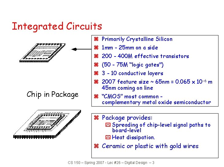
Integrated Circuits z Primarily Crystalline Silicon z 1 mm - 25 mm on a side z 200 - 400 M effective transistors z (50 - 75 M “logic gates") z 3 - 10 conductive layers Chip in Package z 2007 feature size ~ 65 nm = 0. 065 x 10 -6 m 45 nm coming on line z “CMOS” most common complementary metal oxide semiconductor z Package provides: y Spreading of chip-level signal paths to board-level y Heat dissipation. z Ceramic or plastic with gold wires CS 150 – Spring 2007 - Lec #26 – Digital Design – 3
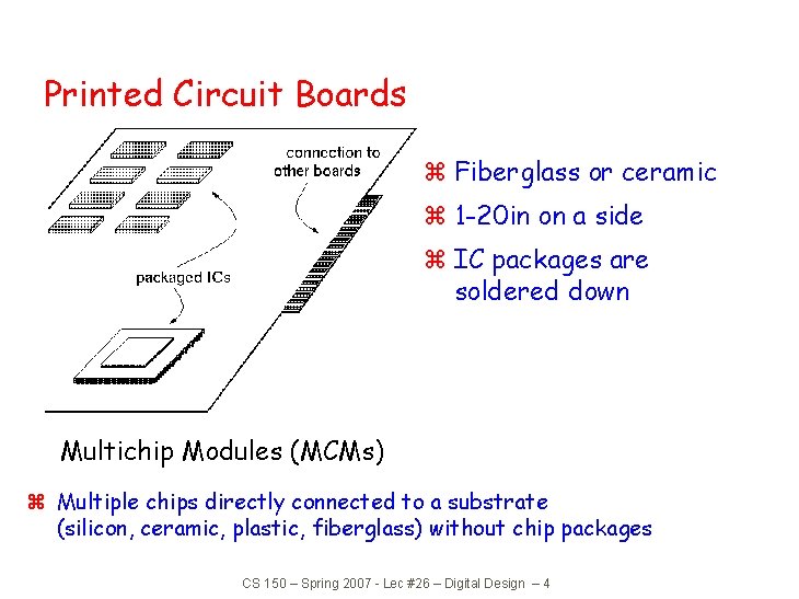
Printed Circuit Boards z Fiberglass or ceramic z 1 -20 in on a side z IC packages are soldered down Multichip Modules (MCMs) z Multiple chips directly connected to a substrate (silicon, ceramic, plastic, fiberglass) without chip packages CS 150 – Spring 2007 - Lec #26 – Digital Design – 4
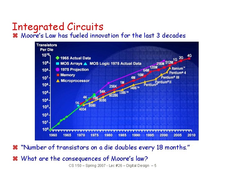
Integrated Circuits z Moore’s Law has fueled innovation for the last 3 decades z “Number of transistors on a die doubles every 18 months. ” z What are the consequences of Moore’s law? CS 150 – Spring 2007 - Lec #26 – Digital Design – 5
Integrated Circuits z Uses for Digital IC technology today: y Standard microprocessors x Used in desktop PCs, and embedded applications (ex: automotive) x Simple system design (mostly software development) y Memory chips (DRAM, SRAM) y Application specific ICs (ASICs) x custom designed to match particular application x can be optimized for low-power, low-cost, high-performance x high-design cost / relatively low manufacturing cost y Field programmable logic devices (FPGAs, CPLDs) x customized to particular application after fabrication x short time to market x relatively high part cost y Standardized low-density components x still manufactured for compatibility with older system designs CS 150 – Spring 2007 - Lec #26 – Digital Design – 6
CMOS Devices z MOSFET (Metal Oxide Semiconductor Field Effect Transistor) Top View Cross Section n. FET The gate acts like a capacitor. A high voltage on the gate attracts charge into the channel. If a voltage exists between the source and drain a current will flow. In its simplest approximation, the device acts like a switch. CS 150 – Spring 2007 - Lec #26 – Digital Design – 7 p. FET
Logic and Layout: NAND Gate CS 150 – Spring 2007 - Lec #26 – Digital Design – 11
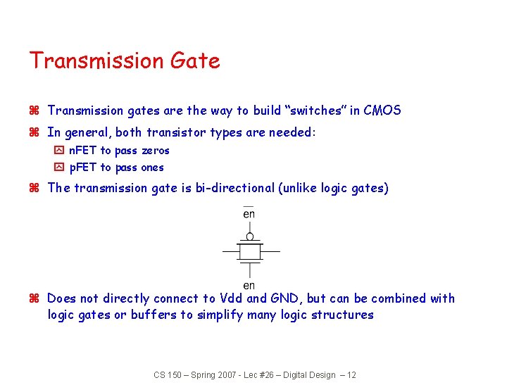
Transmission Gate z Transmission gates are the way to build “switches” in CMOS z In general, both transistor types are needed: y n. FET to pass zeros y p. FET to pass ones z The transmission gate is bi-directional (unlike logic gates) z Does not directly connect to Vdd and GND, but can be combined with logic gates or buffers to simplify many logic structures CS 150 – Spring 2007 - Lec #26 – Digital Design – 12
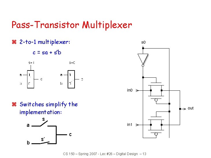
Pass-Transistor Multiplexer z 2 -to-1 multiplexer: c = sa + s’b z Switches simplify the implementation: s a b s’ c CS 150 – Spring 2007 - Lec #26 – Digital Design – 13
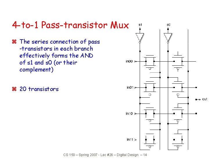
4 -to-1 Pass-transistor Mux z The series connection of pass -transistors in each branch effectively forms the AND of s 1 and s 0 (or their complement) z 20 transistors CS 150 – Spring 2007 - Lec #26 – Digital Design – 14
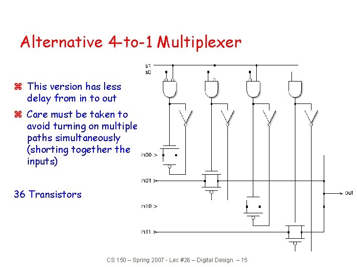
Alternative 4 -to-1 Multiplexer z This version has less delay from in to out z Care must be taken to avoid turning on multiple paths simultaneously (shorting together the inputs) 36 Transistors CS 150 – Spring 2007 - Lec #26 – Digital Design – 15
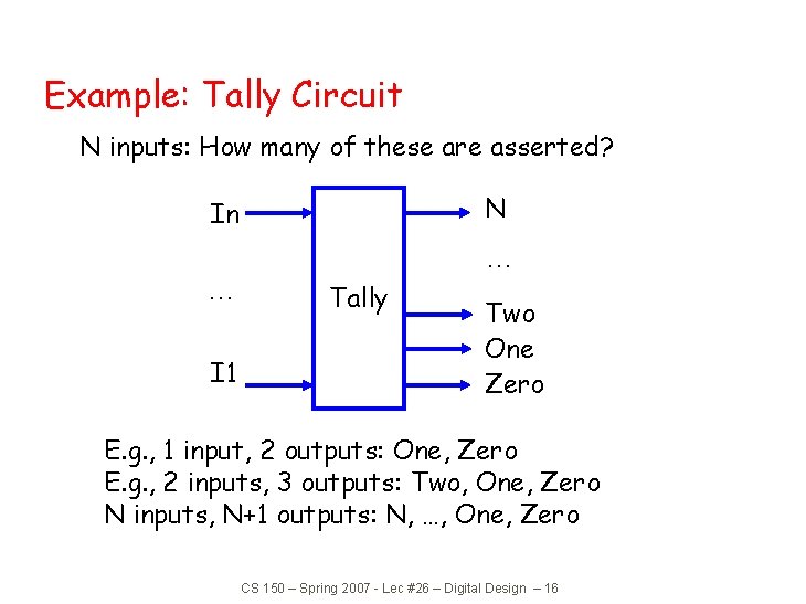
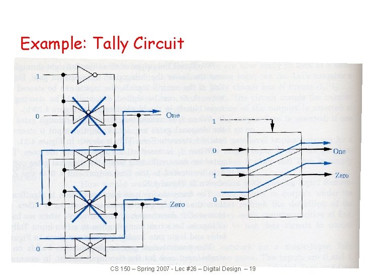
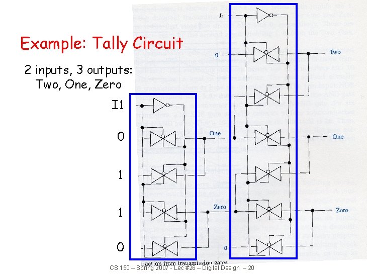
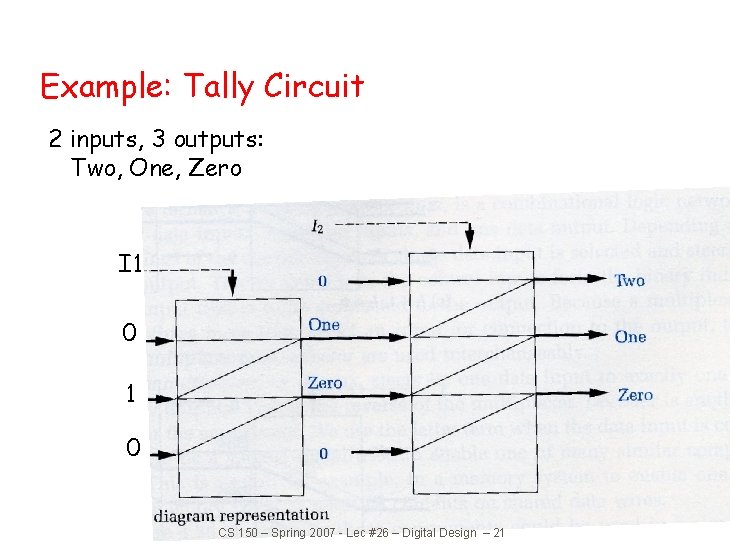
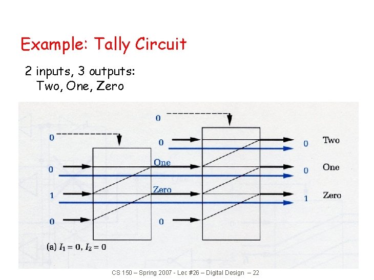
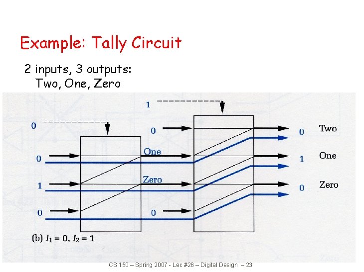
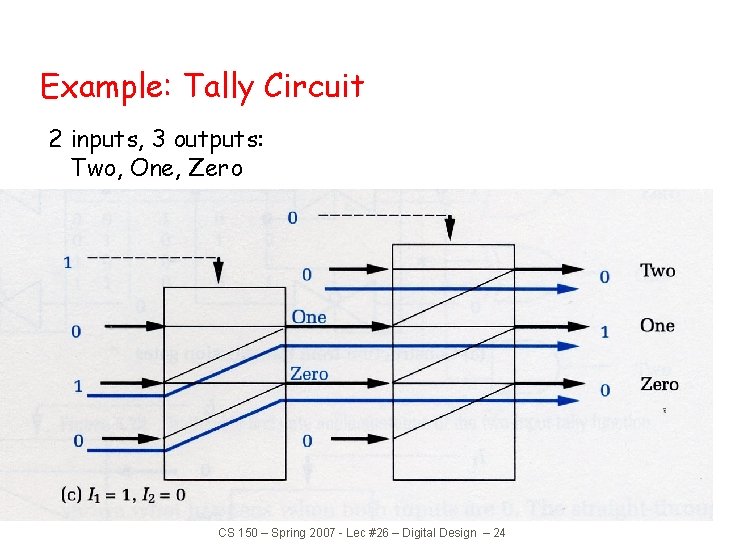
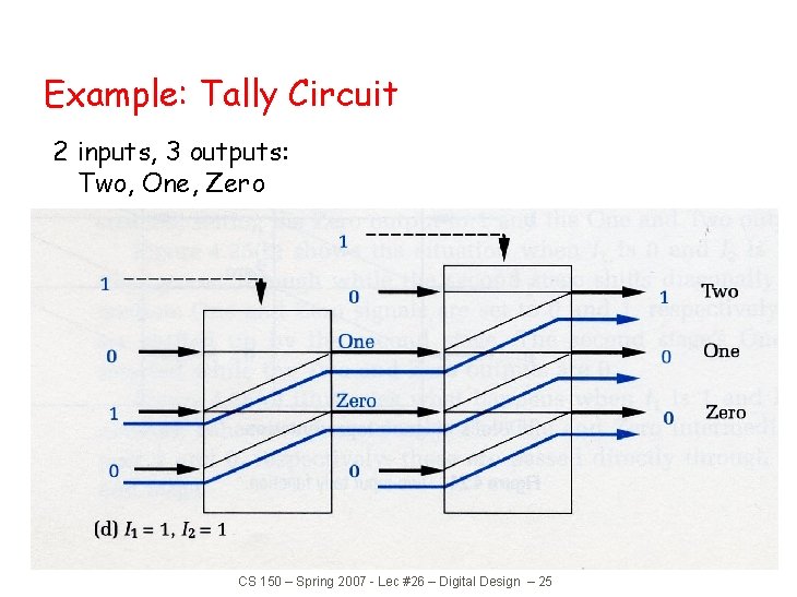
Example: Tally Circuit N inputs: How many of these are asserted? N In … … I 1 Tally Two One Zero E. g. , 1 input, 2 outputs: One, Zero E. g. , 2 inputs, 3 outputs: Two, One, Zero N inputs, N+1 outputs: N, …, One, Zero CS 150 – Spring 2007 - Lec #26 – Digital Design – 16
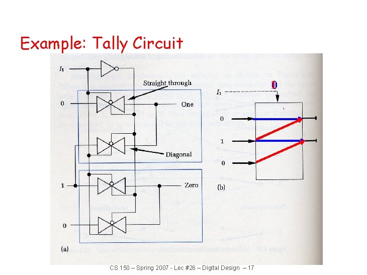
Example: Tally Circuit 10 CS 150 – Spring 2007 - Lec #26 – Digital Design – 17
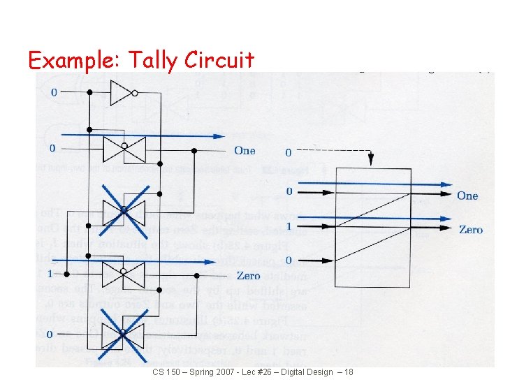
Example: Tally Circuit CS 150 – Spring 2007 - Lec #26 – Digital Design – 18
Example: Tally Circuit CS 150 – Spring 2007 - Lec #26 – Digital Design – 19
Example: Tally Circuit 2 inputs, 3 outputs: Two, One, Zero I 1 0 1 1 0 CS 150 – Spring 2007 - Lec #26 – Digital Design – 20
Example: Tally Circuit 2 inputs, 3 outputs: Two, One, Zero I 1 0 CS 150 – Spring 2007 - Lec #26 – Digital Design – 21
Example: Tally Circuit 2 inputs, 3 outputs: Two, One, Zero CS 150 – Spring 2007 - Lec #26 – Digital Design – 22
Example: Tally Circuit 2 inputs, 3 outputs: Two, One, Zero CS 150 – Spring 2007 - Lec #26 – Digital Design – 23
Example: Tally Circuit 2 inputs, 3 outputs: Two, One, Zero CS 150 – Spring 2007 - Lec #26 – Digital Design – 24
Example: Tally Circuit 2 inputs, 3 outputs: Two, One, Zero CS 150 – Spring 2007 - Lec #26 – Digital Design – 25
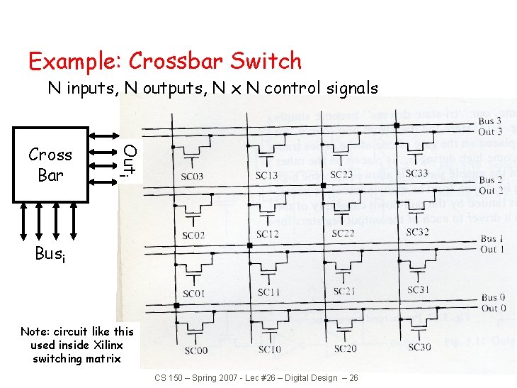
Example: Crossbar Switch N inputs, N outputs, N x N control signals Outi Cross Bar Busi Note: circuit like this used inside Xilinx switching matrix CS 150 – Spring 2007 - Lec #26 – Digital Design – 26
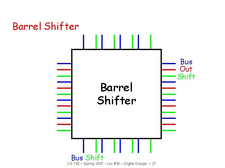
Barrel Shifter Bus Shift CS 150 – Spring 2007 - Lec #26 – Digital Design – 27 Bus Out Shift
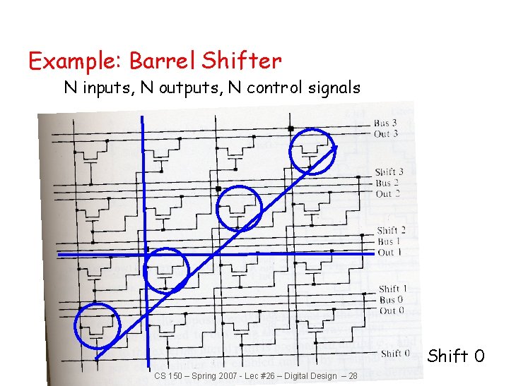
Example: Barrel Shifter N inputs, N outputs, N control signals Shift 0 CS 150 – Spring 2007 - Lec #26 – Digital Design – 28
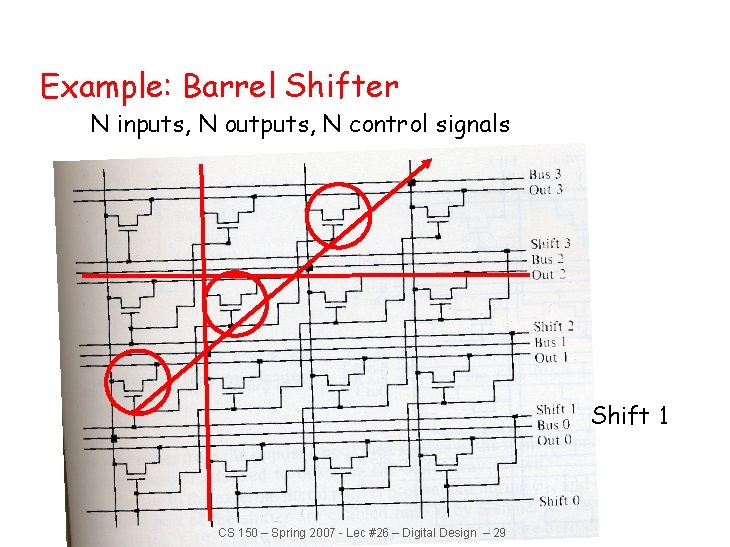
Example: Barrel Shifter N inputs, N outputs, N control signals Shift 1 CS 150 – Spring 2007 - Lec #26 – Digital Design – 29
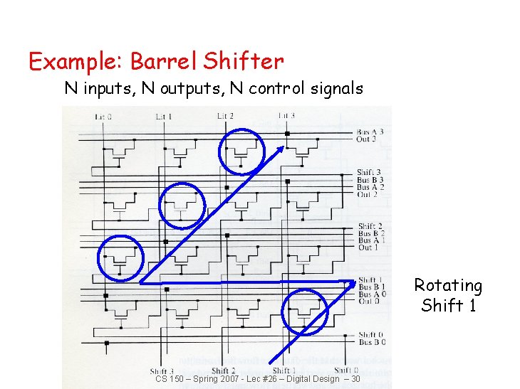
Example: Barrel Shifter N inputs, N outputs, N control signals Rotating Shift 1 CS 150 – Spring 2007 - Lec #26 – Digital Design – 30
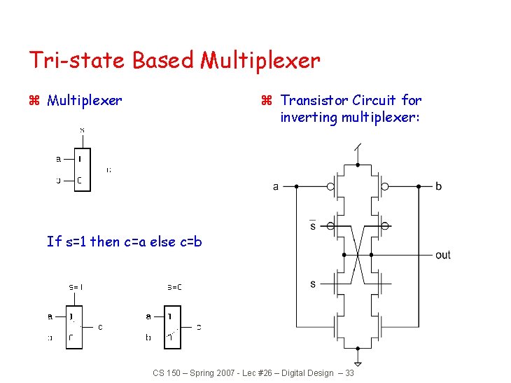
Tri-state Based Multiplexer z Transistor Circuit for inverting multiplexer: If s=1 then c=a else c=b CS 150 – Spring 2007 - Lec #26 – Digital Design – 33
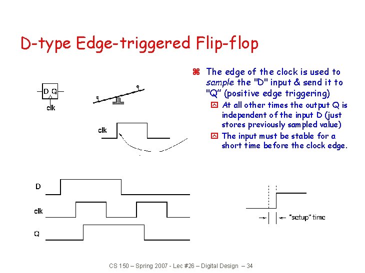
D-type Edge-triggered Flip-flop z The edge of the clock is used to sample the "D" input & send it to "Q” (positive edge triggering) y At all other times the output Q is independent of the input D (just stores previously sampled value) y The input must be stable for a short time before the clock edge. CS 150 – Spring 2007 - Lec #26 – Digital Design – 34
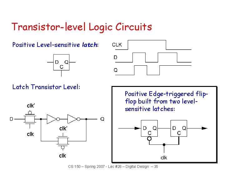
Transistor-level Logic Circuits Positive Level-sensitive latch: Latch Transistor Level: clk’ clk Positive Edge-triggered flipflop built from two levelsensitive latches: clk’ clk CS 150 – Spring 2007 - Lec #26 – Digital Design – 35
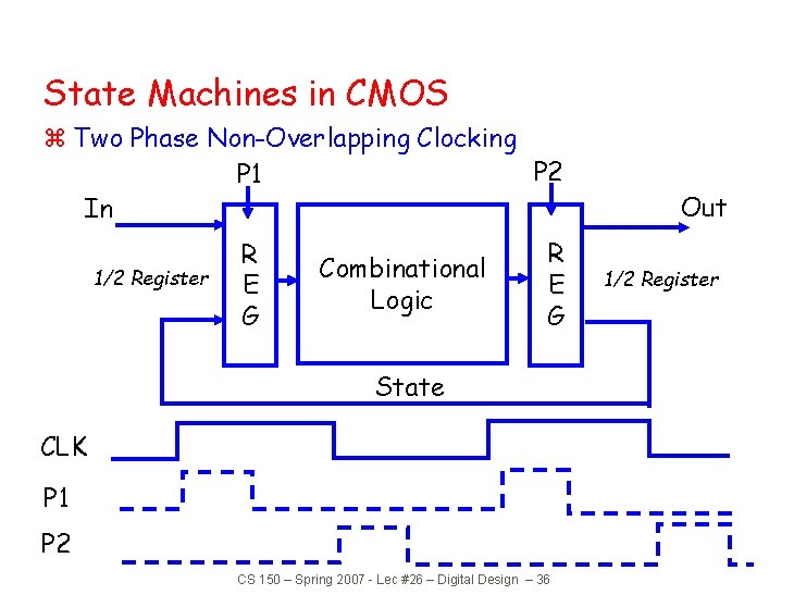
State Machines in CMOS z Two Phase Non-Overlapping Clocking P 2 P 1 In 1/2 Register R E G Combinational Logic R E G State CLK P 1 P 2 CS 150 – Spring 2007 - Lec #26 – Digital Design – 36 Out 1/2 Register
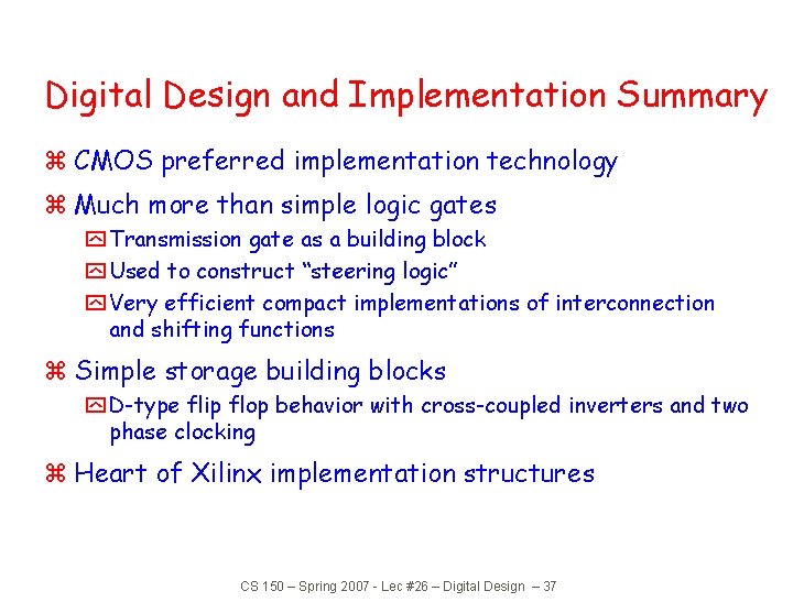
Digital Design and Implementation Summary z CMOS preferred implementation technology z Much more than simple logic gates y Transmission gate as a building block y Used to construct “steering logic” y Very efficient compact implementations of interconnection and shifting functions z Simple storage building blocks y D-type flip flop behavior with cross-coupled inverters and two phase clocking z Heart of Xilinx implementation structures CS 150 – Spring 2007 - Lec #26 – Digital Design – 37