Digital Systems Design 2 Digital Design Ref Digital
- Slides: 30

Digital Systems Design 2 Digital Design Ref. “Digital Design Principles and Practices”, John F. Wakerly, Prentice Hall, 2001, Third Edition Veton Këpuska

Software Aspects of Digital Design u Software Tools are an essential Part of Digital Design n n Hardware Description Languages (HDLs) and accompanying circuit simulation and synthesis tools have changed the landscape of digital design. Computer-Aided Design (CAD) various software tools improve: u u 9/15/2020 Designer’s productivity Correctness and quality of design Veton Këpuska 2

Software Aspects of Digital Design u Classes of Software Tools: n n 9/15/2020 Schematic entry: u It allows schematic diagrams to be drawn online. They check for common errors such as shorted outputs, signals do not go anywhere, etc. HDLs: u Hardware Description Languages, originally were developed for circuit modeling. Now are being used for hardware design. They can be used to design anything from individual function modules to large multi-chip digital systems. Veton Këpuska 3

Software Aspects of Digital Design u HDL compilers, simulators and synthesis tools: A typical HDL software package contains several components: 1. 2. 3. 4. 9/15/2020 In a typical environment the designer writes a text-based “program”, and the HDL compiler analyzes the program for syntax errors. If it compiles correctly the designer has the option of handing it over to a synthesis tool or simulator. Synthesis tool creates a corresponding circuit design targeted to a particular hardware technology. Most often before synthesis designer will use the compiler’s results as input to a simulator to verify the behavior of the design. Veton Këpuska 4

Software Aspects of Digital Design n 9/15/2020 Simulator. u Help designers to predict the electrical and functional behavior of a chip without actually building it, allowing most if not all bugs to be found before the chip is fabricated. u Simulators are also used in the design of “programmable logic devices, ” and in the overall design of systems that incorporate many individual components. They are somewhat less critical in this case because it’s easier for the designer to make changes in components and interconnections on a printed-circuit board. Veton Këpuska 5

Software Aspects of Digital Design n 9/15/2020 Test benches. Software environments that are used by designers to formalize circuit simulation and testing. u The idea is to build a a set of programs around a design to automatically exercise its functions and check both its functional and its timing behavior. u This is especially useful when small design changes are made- the test bench can be run to ensure that bug fixes or “improvements” in one area do not break something else. u Test-bench programs may be written in the same HDL as the design itself, in C or C++, or in combination of languages including scripting languages like Perl. Veton Këpuska 6

Software Aspects of Digital Design n Timing analyzers and verifiers. u u 9/15/2020 The time dimension is very important in digital design. All digital circuits take time to produce a new output value in response to an input change. Much of a designer’s effort is spent ensuring that such output changes occur quickly enough (or in some cases not to quickly). Specialized programs can automate the tedious task of drawing timing diagrams and specifying and verifying the timing relationships between different signals in a complex system. Veton Këpuska 7

Software Aspects of Digital Design n Specialized programs. u u They can be written in a high-level programming language like C or C++, or scripts in languages like Perl to solve particular design problems. Although CAD tools are important they “don’t make or break a digital designer” (similarly as a fast typists not necessarily makes a great writer). 9/15/2020 Veton Këpuska 8

Integrated Circuits (IC) u A collection of one or more gates fabricated on a single silicon chip is called an integrated circuit. n n 9/15/2020 IC initially is part of a much larger circular plate called wafer. A number of IC’s a fabricated at the same time in one wafer. One IC in a wafer is called a die. Each die is mounted in a package. The pads of a die are connected to the package pins which makes the IC. IC are used to refer to silicon die or chip to refer to the same think. Veton Këpuska 9

Integrated Circuits (IC) u Small-Scale Integration (SSI): n n n u Typically they contain a handful of gates or flipflops, the basic building blocks of digital design. They usually come in dual in-line-pin (DIP) package. Example: 7400 -series of SSI ICs Medium-Scale Integration (MSI): n n n 9/15/2020 Contains the equivalent of about 20 -200 gates. Typically it contains a functional building block, such as a decoder, register, or counter. Equivalent building blocks are used extensively in the design of large ICs. Veton Këpuska 10

Integrated Circuits (IC) u u Large-Scale Integration (LSI): n Contain equivalent of 200 – 200, 000 gates or more. LSI parts include small memories, microprocessors, programmable logic devices, and customized devices. n Dividing line between LSI and very large-scale integration (VLSI) is fuzzy and tends to be stated in terms of transistor count rather than gate count. Very Large-Scale Integration (VLSI): n Any IC with over 1, 000 transistors is definitely VLSI. n Now days it includes most microprocessors and memories as well as larger programmable logic devices and customized devices. n In 1999 VLSI ICs with as many as 50 million transistors were being designed. 9/15/2020 Veton Këpuska 11

Programmable Logic Devices u u There a wide variety of ICs that can have their logic function “programmed” into them after they are manufactured. Most of these devices use technology that also allows the function to be reprogrammed. Reprogrammability allows bug fixes to be made to the original design. This may mean that the fix can be done without physically replacing or rewiring the device. 9/15/2020 Veton Këpuska 12

Programmable Logic Devices u Programmable Logic Arrays (PLAs) n n n 9/15/2020 Historically they are the first programmable logic devices. PLSs contained two-level structure of AND and OR gates with user-programmable connections. Using this structure a designer could accommodate any logic function up to a certain level of complexity using the wellknown theory of logic synthesis and minimization. PLA structure was enhanced and PLA costs were reduced with the introduction of programmable array logic (PAL) devices. Today such devices are generically called programmable logic devices (PLDs) and are the “MSI” of the programmable logic industry. The ever-increasing capacity of integrated circuits created an opportunity of IC manufactures to design larger PLDs for larger digital-design applications. For technical reasons the basic twolevel AND-OR structure of PLDs could not be scaled to larger sizes. Instead, IC manufacturers devised complex PLD (CPLD) architectures to achieve the required scale. Veton Këpuska 13

Programmable Logic Devices u Complex Programmable Logic Devices (CPLD). n n n 9/15/2020 A typical CPLD is merely a collection of multiple PLDs and an interconnection structure, all on the same chip. In addition to the individual PLDs, the on-chip interconnection structure is also programmable providing a rich variety of design possibilities. CPLDs can be scaled to larger sizes by increasing the number of individual PLDS and the richness of the interconnection structure of the CPLD chip. Veton Këpuska 14

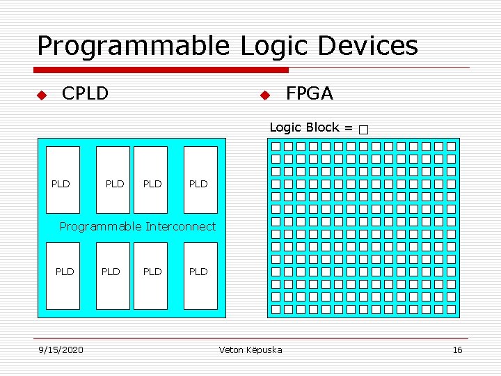
Programmable Logic Devices u Field-Programmable Gate Arrays (FPGA) n 9/15/2020 At about the same time that CPLDs were being invented, other IC manufacturers took a different approach to scaling the size of programmable logic chips. FPGA as compared to CPLDs contain a much larger number of smaller individual logic blocks and provides a large, distributed interconnection structure that dominates the entire chip. The Figure 1. illustrated the difference between the two chipdesign approaches. Veton Këpuska 15

Programmable Logic Devices u CPLD u FPGA Logic Block = PLD PLD Programmable Interconnect PLD 9/15/2020 PLD PLD Veton Këpuska 16

Programmable Logic Devices u u Xilinx Inc. (largest manufacturer of large programmable logic devices) acknowledges that there is a place for both approaches and it manufactures both type of devices. What is more important than chip architecture is that both approaches support a style of design in which products can be moved from design concept to prototype and production in a very short time. Also important in achieving short “time-to-market” for all kinds of PLD based products is the use of HDLs in their design. Languages like VHDL, Verilog, ABEL and their accompanying software tools, allow a design to be compiled, synthesized, and downloaded into a PLD, CPLD, or FPGA literally in minutes. The power of highly structured, hierarchical languages like VHDL is especially important in helping designers to utilize the hundreds of thousands or millions of gates that provided in the largest CPLDs and FPGAs. 9/15/2020 Veton Këpuska 17

Application Specific ICs (ASICs) u u Perhaps the most interesting developments in IC technology for the average digital designer are not the ever-increasing chip sizes, but the ever-increasing opportunities to “design your own chip”. Chips designed for a particular, limited product or application are called semi-custom ICs or application-specific ICs (ASICs). ASICs generally reduce the total component and manufacturing cost of a product by reducing chip count, physical size, and power consumption, and they often provide higher performance. 9/15/2020 Veton Këpuska 18

Application Specific ICs (ASICs) u u u The nonrecurring engineering (NRE) cost for designing an ASIC can exceed the cost of a discrete design by $5, 000 to $250, 000 or more. NRE charges are paid to the IC manufacturer and others who are responsible for designing the internal structure of the chip, creating tooling such as the metal masks for manufacturing the chips, developing tests for the manufactured chips, and actually making the first few sample chips. The NRE cost for a typical, medium-complexity ASIC with about 100, 000 gates is $30, 000 -$50, 000. An ASIC design normally makes sense only when the NRE cost can be offset by the per-unit savings over the expected sales volume of the product. The NRE cost to design a custom LSI chip – a chip whose functions, internal architecture, and detailed transistor-level design is tailored for a specific customer – is very high $250, 000 or more. Thus full custom LSI design is done only for chips that have general commercial application or that will enjoy very high sales volume in a specific application (e. g. , a digital watch chip, a network interface, or a bus-interface circuit for a PC). 9/15/2020 Veton Këpuska 19

Application Specific ICs (ASICs) u Reduction of NRE cost: n IC manufacturers have developed libraries of standard cells including commonly used MSI functions such as: u u u Decoders, Registers, and Counters and commonly used LSI functions such as: u u u 9/15/2020 Memories, Programmable Logic Arrays, and Microprocessors. Veton Këpuska 20

Application Specific ICs (ASICs) u Standard-Cell Design n n 9/15/2020 Logic designer interconnects functions in much the same way as in a multi-chip MSI/LSI design. Custom cells are created only if absolutely necessary. All of the cells are then laid out on the chip, optimizing the layout to reduce propagation delays and minimize the size of the chip. Minimizing the chip size reduces the per-unit cost of the chip, since it increases the number of chips that can be fabricated on a single wafer. The NRE cost for a standard-cell design is typically on the order of $150, 000. Veton Këpuska 21

Application Specific ICs (ASICs) u u IC manufacturers have gone step further to bring ASIC design capability to the masses since $150, 000 is still a lot of money for most people/companies. Gate-Array is an IC whose internal structure is an array of gates whose interconnections are initially unspecified. n n u The logic designer specifies the gate types and interconnections. Even though the chip design is ultimately specified at this very low level, the designer typically works with “macro-cells”, the same highlevel functions used in multi-chip MSI/LSI and standard-cell designs; software expands the high-level design into a low-level one. Main difference between standard-cell and gate-array design is that: n n n 9/15/2020 Macro-cells and the chip layout of a gate array are not as highly optimized as those in standard-cell design, so the chip may be 25% or more larger and therefore may cost more. There is no opportunity to create custom cells in the gate-array approach. On the other hand gate-array design can be finished faster and at a lower NRE cost, ranging from about $5000 (what you are told initially) to $75, 000 (what you find out you have spend when you are all done). Veton Këpuska 22

Application Specific ICs (ASICs) u Basic Digital Design Methods covered in the class apply very well to the functional design of ASICs as well. However, there additional: n n n u Opportunities, Constraints, and Steps in ASIC design. It depends usually on the particular ASIC vendor and design environment used. 9/15/2020 Veton Këpuska 23

Printed-Circuit Boards u u An IC is normally mounted on a printed-circuit board (PCB) that connects it to other ICs in a system. Multilayer PCBs used in typical digital systems have copper wiring etched on multiple, thin layers of fiberglass that are laminated into a single board about 1/16 inch think PCB traces – individual wire connections are usually quite narrow, 10 -25 mils typically (1 mil = 1/1000 inch). In Fine-line PCB technology the traces are extremely narrow, as little as 4 mils wide with 4 mils spacing between adjacent traces. Thus, up to 125 connections may be routed in a one-inch-wide band on a single layer of the PCB. If higher connection density is needed them more layers are required. 9/15/2020 Veton Këpuska 24

Printed-Circuit Boards u Surface-Mount Technology (SMT) is the most common technology used in modern PCBs: n Instead of having long pins of DIP packages that poke through the board and are soldered to the underside: u u 9/15/2020 The leads of SMT IC packages are bent to make flat contact with the top surface of the PCB. Before components are mounted on the PCB, a special “solder paste” is applied to contact pads on the PCB using a stencil whose hole pattern matches the contact pads to be soldered. The SMT components are placed on the pads, where they are held in place by the solder paste (or by glue in some cases) Finally the entire assembly is passed through an oven to melt the solder paste which then solidifies when cooled. Veton Këpuska 25

Printed-Circuit Boards u u Surface-mount component technology, coupled with fine-line PCB technology, allows extremely dense packing of integrated circuits and other components on PCB. For very high-speed circuits, dense packing goes a long way toward minimizing adverse analog phenomena, including transmissionline effects and speed-of-light limitations. 9/15/2020 Veton Këpuska 26

Printed-Circuit Boards u To satisfy most stringent requirements for speed and density, multi-chip modules (MCMs) have been developed. n n n 9/15/2020 In this technology, IC dice (plural for die), are not mounted in individual plastic or ceramic packages, instead The IC dice for a high-speed subsystem (e. g. , a processor and high-speed memory), are bonded directly to a substrate that contains the required interconnections on the multiple layers. The MCM is hermetically sealed and has its own external pins for power, ground, and just those signals that are required by the system that contains it. Veton Këpuska 27

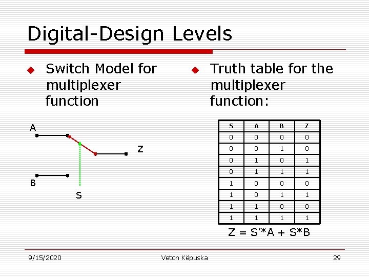
Digital-Design Levels u u u Digital Design can be carried out at several different levels of representation and abstraction. Although, one may learn and practice design at a particular level, from time to time it is needed to go up or down a level or two to get the job done. In industry the most designers have been steadily moving to higher levels of abstraction as circuit density and functionality have increased. The lowest level of digital design is device physics and IC manufacturing processes. This is the level that is primarily responsible for the breathtaking advances in IC speed and density that have occurred over the past decades. The effects of these advances are summarized in Moore’s Law, first stated by Intel founder Gordon Moore in 1965: n n u The number of transistors per square inch in an IC doubles every year. In recent years the rate of advance has slowed down to doubling about every 18 months, but it is important to note that with each doubling of density has come the doubling of speed. To get the importance of the need to design a module at a different level consider the example of multiplexer: n 9/15/2020 Assume a multiplexer with two data input bits A and B, a control input bit S, and an output bit Z as depicted in Figure 2. Veton Këpuska 28

Digital-Design Levels u Switch Model for multiplexer function u A Z B S Truth table for the multiplexer function: S A B Z 0 0 0 1 0 1 1 0 0 0 1 1 1 1 0 0 1 1 Z = S’*A + S*B 9/15/2020 Veton Këpuska 29

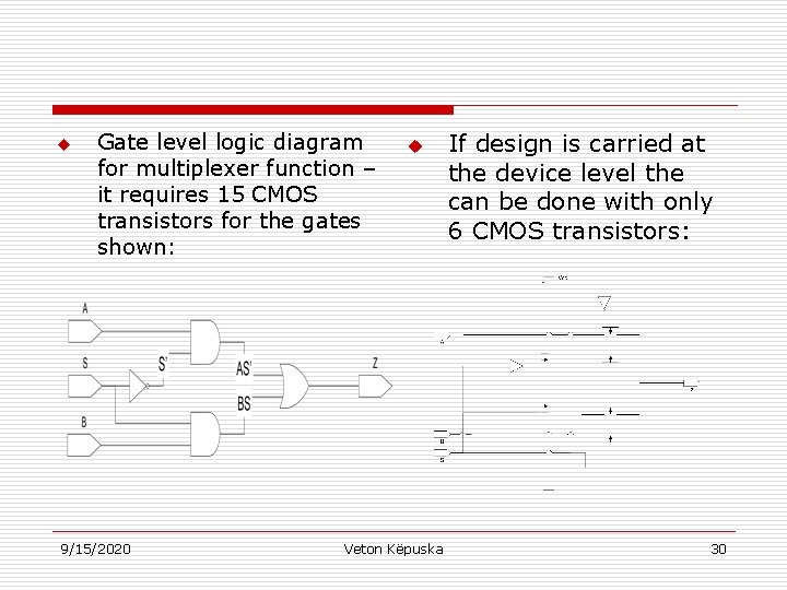
u Gate level logic diagram for multiplexer function – it requires 15 CMOS transistors for the gates shown: 9/15/2020 u Veton Këpuska If design is carried at the device level the can be done with only 6 CMOS transistors: 30