CSE 477 VLSI Digital Circuits Fall 2003 Lecture

- Slides: 33

CSE 477 VLSI Digital Circuits Fall 2003 Lecture 03: MOS Transistor Mary Jane Irwin ( www. cse. psu. edu/~mji ) www. cse. psu. edu/~cg 477 [Adapted from Rabaey’s Digital Integrated Circuits, Second Edition, © 2003 Rabaey, A. Chandrakasan, B. Nikolic] CSE 477 L 03 MOS Transistor. 1 J. Irwin&Vijay, PSU, 2003

Course Administration q Instructor: Mary Jane Irwin mji@cse. psu. edu www. cse. psu. edu/~mji 227 Pond Lab Office Hrs: T 16: 00 -17: 00 & W 9: 30 -10: 45 q TA: q Labs: Accounts on 101 Pond Lab machines q URL: www. cse. psu. edu/~cg 477 q Text: Digital Integrated Circuits, 2 nd Edition Rabaey et. al. , © 2003 q Slides: pdf on the course web page after lecture Feihui Li feli@cse. psu. edu 128 Hammond Office Hrs: TBD CSE 477 L 03 MOS Transistor. 2 Greg Link link@cse. psu. edu 226 Pond Lab TBD Irwin&Vijay, PSU, 2003

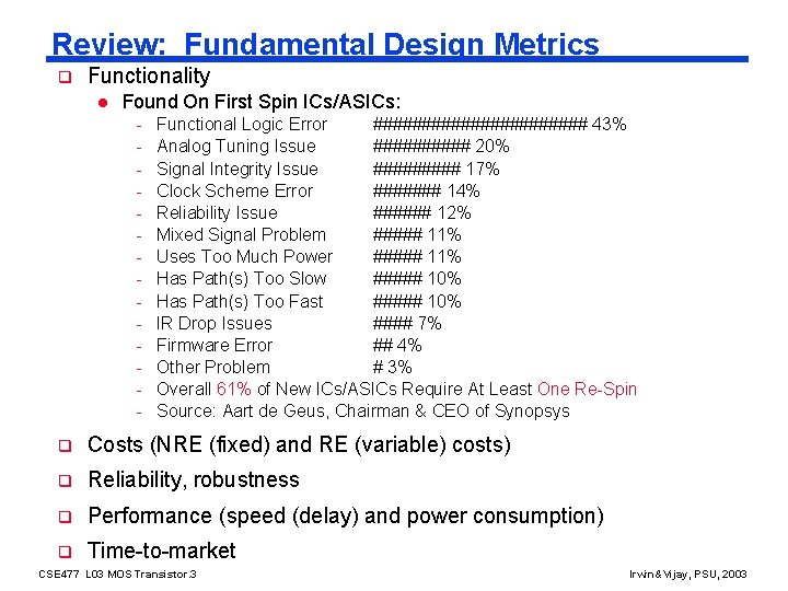
Review: Fundamental Design Metrics q Functionality l Found On First Spin ICs/ASICs: - Functional Logic Error ########### 43% Analog Tuning Issue ##### 20% Signal Integrity Issue ##### 17% Clock Scheme Error ####### 14% Reliability Issue ###### 12% Mixed Signal Problem ##### 11% Uses Too Much Power ##### 11% Has Path(s) Too Slow ##### 10% Has Path(s) Too Fast ##### 10% IR Drop Issues #### 7% Firmware Error ## 4% Other Problem # 3% Overall 61% of New ICs/ASICs Require At Least One Re-Spin Source: Aart de Geus, Chairman & CEO of Synopsys q Costs (NRE (fixed) and RE (variable) costs) q Reliability, robustness q Performance (speed (delay) and power consumption) q Time-to-market CSE 477 L 03 MOS Transistor. 3 Irwin&Vijay, PSU, 2003

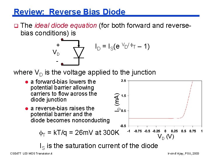
Review: Reverse Bias Diode q The ideal diode equation (for both forward and reversebias conditions) is + VD - ID = IS(e VD/ T – 1) l l a forward-bias lowers the potential barrier allowing carriers to flow across the diode junction a reverse-bias raises the potential barrier and the diode becomes nonconducting ID (m. A) where VD is the voltage applied to the junction T = k. T/q = 26 m. V at 300 K VD (V) IS is the saturation current of the diode CSE 477 L 03 MOS Transistor. 4 Irwin&Vijay, PSU, 2003

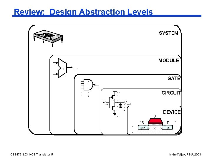
Review: Design Abstraction Levels SYSTEM MODULE + GATE CIRCUIT Vin Vout G S n+ CSE 477 L 03 MOS Transistor. 5 DEVICE D n+ Irwin&Vijay, PSU, 2003

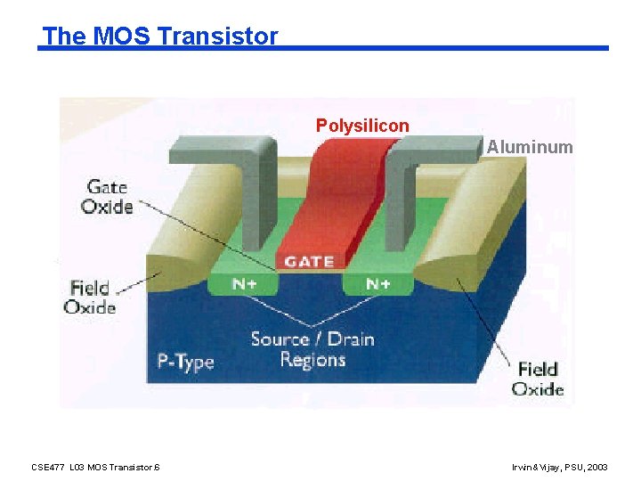
The MOS Transistor Polysilicon Aluminum CSE 477 L 03 MOS Transistor. 6 Irwin&Vijay, PSU, 2003

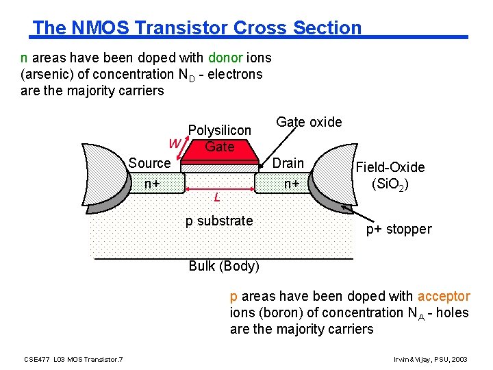
The NMOS Transistor Cross Section n areas have been doped with donor ions (arsenic) of concentration ND - electrons are the majority carriers Polysilicon W Gate Source n+ L p substrate Gate oxide Drain n+ Field-Oxide (Si. O 2) p+ stopper Bulk (Body) p areas have been doped with acceptor ions (boron) of concentration NA - holes are the majority carriers CSE 477 L 03 MOS Transistor. 7 Irwin&Vijay, PSU, 2003

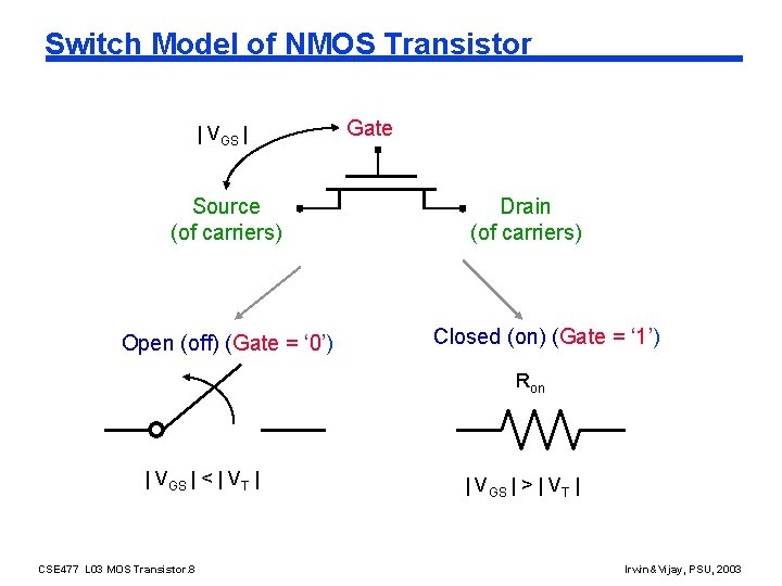
Switch Model of NMOS Transistor | VGS | Source (of carriers) Open (off) (Gate = ‘ 0’) Gate Drain (of carriers) Closed (on) (Gate = ‘ 1’) Ron | VGS | < | VT | CSE 477 L 03 MOS Transistor. 8 | VGS | > | VT | Irwin&Vijay, PSU, 2003

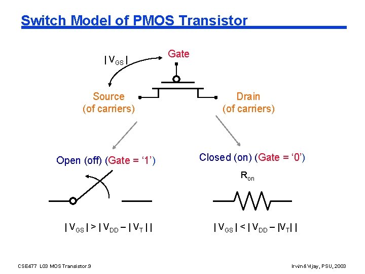
Switch Model of PMOS Transistor | VGS | Source (of carriers) Open (off) (Gate = ‘ 1’) Gate Drain (of carriers) Closed (on) (Gate = ‘ 0’) Ron | VGS | > | VDD – | VT | | CSE 477 L 03 MOS Transistor. 9 | VGS | < | VDD – |VT| | Irwin&Vijay, PSU, 2003

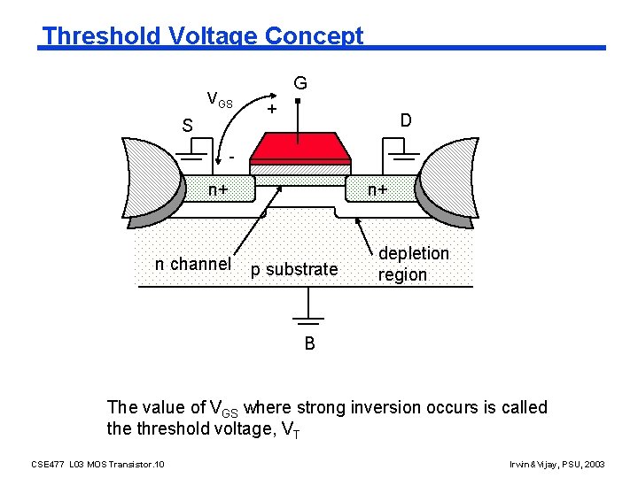
Threshold Voltage Concept VGS S G + D - n+ n+ n channel p substrate depletion region B The value of VGS where strong inversion occurs is called the threshold voltage, VT CSE 477 L 03 MOS Transistor. 10 Irwin&Vijay, PSU, 2003

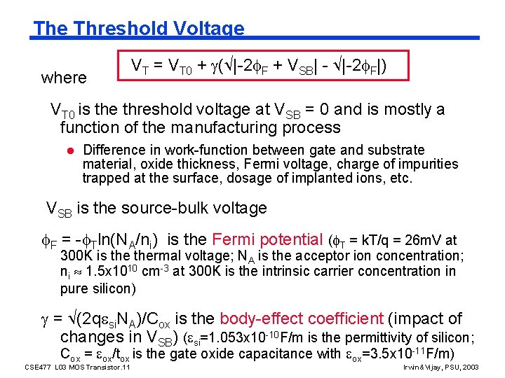
The Threshold Voltage where VT = VT 0 + ( |-2 F + VSB| - |-2 F|) VT 0 is the threshold voltage at VSB = 0 and is mostly a function of the manufacturing process l Difference in work-function between gate and substrate material, oxide thickness, Fermi voltage, charge of impurities trapped at the surface, dosage of implanted ions, etc. VSB is the source-bulk voltage F = - Tln(NA/ni) is the Fermi potential ( T = k. T/q = 26 m. V at 300 K is thermal voltage; NA is the acceptor ion concentration; ni 1. 5 x 1010 cm-3 at 300 K is the intrinsic carrier concentration in pure silicon) = (2 q si. NA)/Cox is the body-effect coefficient (impact of changes in VSB) ( si=1. 053 x 10 -10 F/m is the permittivity of silicon; Cox = ox/tox is the gate oxide capacitance with ox=3. 5 x 10 -11 F/m) CSE 477 L 03 MOS Transistor. 11 Irwin&Vijay, PSU, 2003

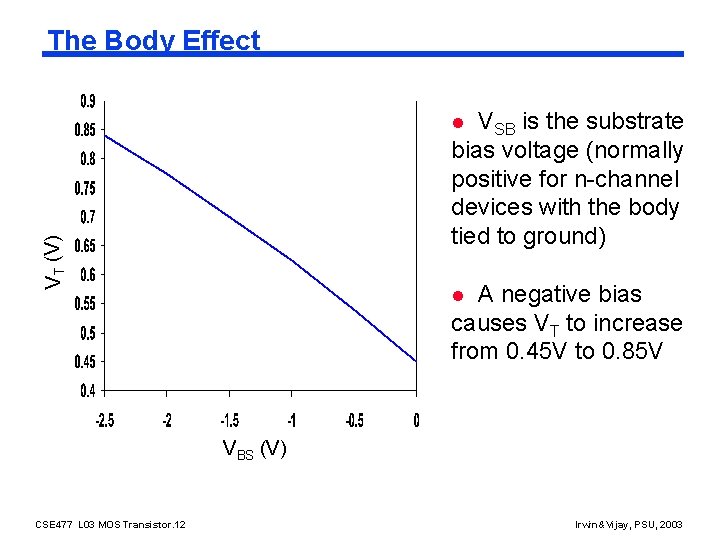
The Body Effect VSB is the substrate bias voltage (normally positive for n-channel devices with the body tied to ground) VT (V) l A negative bias causes VT to increase from 0. 45 V to 0. 85 V l VBS (V) CSE 477 L 03 MOS Transistor. 12 Irwin&Vijay, PSU, 2003

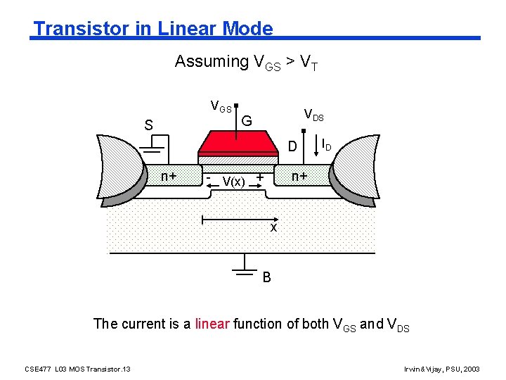
Transistor in Linear Mode Assuming VGS > VT VGS S VDS G D n+ ID n+ - V(x) + x B The current is a linear function of both VGS and VDS CSE 477 L 03 MOS Transistor. 13 Irwin&Vijay, PSU, 2003

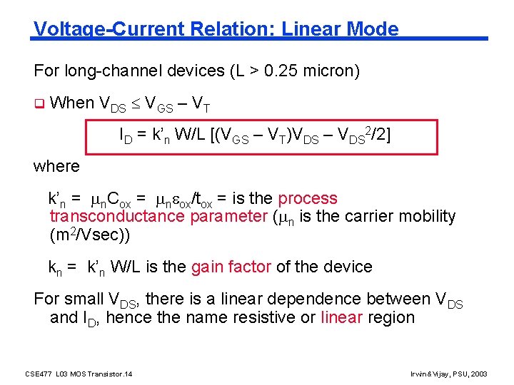
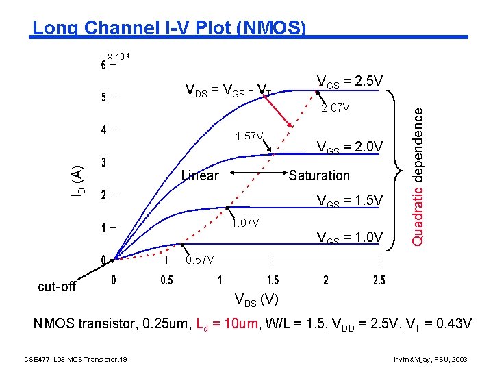
Voltage-Current Relation: Linear Mode For long-channel devices (L > 0. 25 micron) q When VDS VGS – VT ID = k’n W/L [(VGS – VT)VDS – VDS 2/2] where k’n = n. Cox = n ox/tox = is the process transconductance parameter ( n is the carrier mobility (m 2/Vsec)) kn = k’n W/L is the gain factor of the device For small VDS, there is a linear dependence between VDS and ID, hence the name resistive or linear region CSE 477 L 03 MOS Transistor. 14 Irwin&Vijay, PSU, 2003

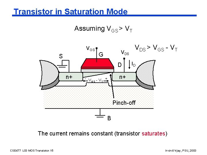
Transistor in Saturation Mode Assuming VGS > VT VGS S VDS G D n+ VDS > VGS - VT ID n+ - V -V + GS T Pinch-off B The current remains constant (transistor saturates) CSE 477 L 03 MOS Transistor. 15 Irwin&Vijay, PSU, 2003

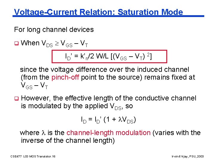
Voltage-Current Relation: Saturation Mode For long channel devices q When VDS VGS – VT ID’ = k’n/2 W/L [(VGS – VT) 2] since the voltage difference over the induced channel (from the pinch-off point to the source) remains fixed at VGS – VT q However, the effective length of the conductive channel is modulated by the applied VDS, so ID = ID’ (1 + VDS) where is the channel-length modulation (varies with the inverse of the channel length) CSE 477 L 03 MOS Transistor. 16 Irwin&Vijay, PSU, 2003

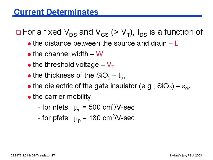
Current Determinates q For l a fixed VDS and VGS (> VT), IDS is a function of the distance between the source and drain – L the channel width – W l the threshold voltage – VT l the thickness of the Si. O 2 – tox l the dielectric of the gate insulator (e. g. , Si. O 2) – ox l the carrier mobility - for nfets: n = 500 cm 2/V-sec - for pfets: p = 180 cm 2/V-sec l CSE 477 L 03 MOS Transistor. 17 Irwin&Vijay, PSU, 2003

Long Channel I-V Plot (NMOS) X 10 -4 VGS = 2. 5 V 2. 07 V ID (A) 1. 57 V Linear VGS = 2. 0 V Saturation VGS = 1. 5 V 1. 07 V VGS = 1. 0 V Quadratic dependence VDS = VGS - VT 0. 57 V cut-off VDS (V) NMOS transistor, 0. 25 um, Ld = 10 um, W/L = 1. 5, VDD = 2. 5 V, VT = 0. 43 V CSE 477 L 03 MOS Transistor. 19 Irwin&Vijay, PSU, 2003

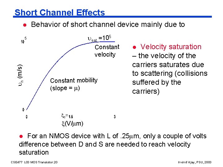
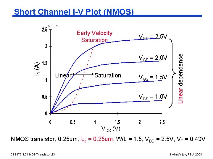
Short Channel Effects l Behavior of short channel device mainly due to sat =105 Constant velocity n (m/s) 5 Constant mobility (slope = ) Velocity saturation – the velocity of the carriers saturates due to scattering (collisions suffered by the carriers) l c= (V/ m) l For an NMOS device with L of. 25 m, only a couple of volts difference between D and S are needed to reach velocity saturation CSE 477 L 03 MOS Transistor. 20 Irwin&Vijay, PSU, 2003

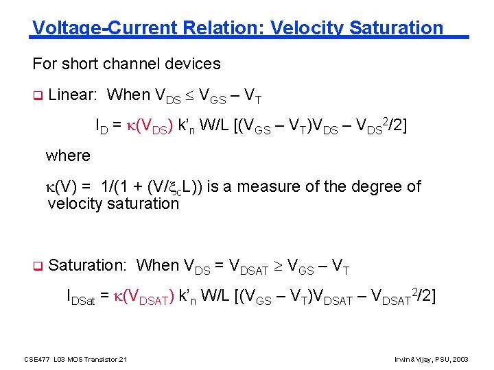
Voltage-Current Relation: Velocity Saturation For short channel devices q Linear: When VDS VGS – VT ID = (VDS) k’n W/L [(VGS – VT)VDS – VDS 2/2] where (V) = 1/(1 + (V/ c. L)) is a measure of the degree of velocity saturation q Saturation: When VDS = VDSAT VGS – VT IDSat = (VDSAT) k’n W/L [(VGS – VT)VDSAT – VDSAT 2/2] CSE 477 L 03 MOS Transistor. 21 Irwin&Vijay, PSU, 2003

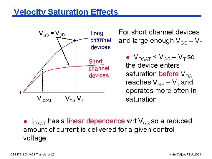
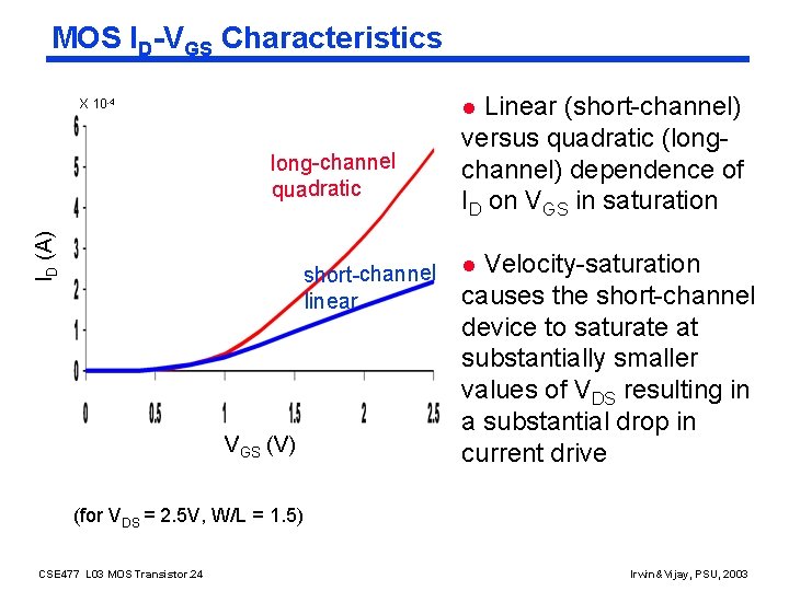
Velocity Saturation Effects VGS = VDD Long channel devices Short channel devices VDSAT VGS-VT For short channel devices and large enough VGS – VT VDSAT < VGS – VT so the device enters saturation before VDS reaches VGS – VT and operates more often in saturation l IDSAT has a linear dependence wrt VGS so a reduced amount of current is delivered for a given control voltage l CSE 477 L 03 MOS Transistor. 22 Irwin&Vijay, PSU, 2003

Short Channel I-V Plot (NMOS) X 10 -4 VGS = 2. 5 V ID (A) VGS = 2. 0 V Linear Saturation VGS = 1. 5 V VGS = 1. 0 V Linear dependence Early Velocity Saturation VDS (V) NMOS transistor, 0. 25 um, Ld = 0. 25 um, W/L = 1. 5, VDD = 2. 5 V, VT = 0. 43 V CSE 477 L 03 MOS Transistor. 23 Irwin&Vijay, PSU, 2003

MOS ID-VGS Characteristics Linear (short-channel) versus quadratic (longchannel) dependence of ID on VGS in saturation l X 10 -4 ID (A) long-channel quadratic short-channel linear VGS (V) Velocity-saturation causes the short-channel device to saturate at substantially smaller values of VDS resulting in a substantial drop in current drive l (for VDS = 2. 5 V, W/L = 1. 5) CSE 477 L 03 MOS Transistor. 24 Irwin&Vijay, PSU, 2003

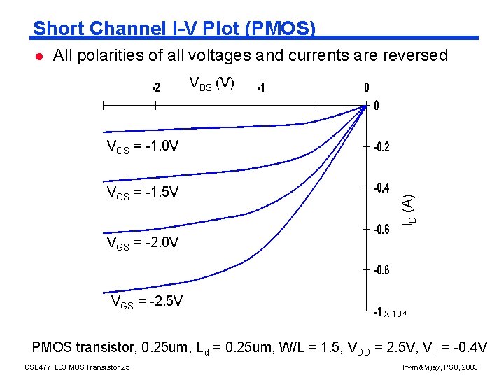
Short Channel I-V Plot (PMOS) l All polarities of all voltages and currents are reversed VDS (V) VGS = -1. 5 V ID (A) VGS = -1. 0 V VGS = -2. 5 V X 10 -4 PMOS transistor, 0. 25 um, Ld = 0. 25 um, W/L = 1. 5, VDD = 2. 5 V, VT = -0. 4 V CSE 477 L 03 MOS Transistor. 25 Irwin&Vijay, PSU, 2003

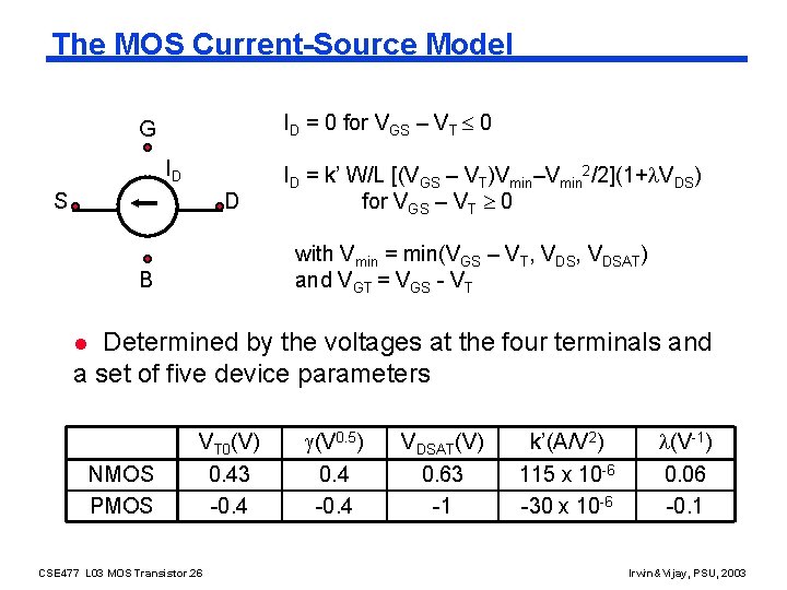
The MOS Current-Source Model ID = 0 for VGS – VT 0 G ID S D ID = k’ W/L [(VGS – VT)Vmin–Vmin 2/2](1+ VDS) for VGS – VT 0 with Vmin = min(VGS – VT, VDSAT) and VGT = VGS - VT B Determined by the voltages at the four terminals and a set of five device parameters l NMOS PMOS VT 0(V) 0. 43 -0. 4 CSE 477 L 03 MOS Transistor. 26 (V 0. 5) 0. 4 -0. 4 VDSAT(V) 0. 63 -1 k’(A/V 2) 115 x 10 -6 -30 x 10 -6 (V-1) 0. 06 -0. 1 Irwin&Vijay, PSU, 2003

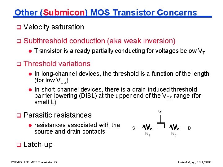
Other (Submicon) MOS Transistor Concerns q Velocity saturation q Subthreshold conduction (aka weak inversion) l q q Threshold variations l In long-channel devices, the threshold is a function of the length (for low VDS) l In short-channel devices, there is a drain-induced threshold barrier lowering (DIBL) at the upper end of the VDS range (for small L) G Parasitic resistances l q Transistor is already partially conducting for voltages below VT resistances associated with the source and drain contacts S D RS RD Latch-up CSE 477 L 03 MOS Transistor. 27 Irwin&Vijay, PSU, 2003

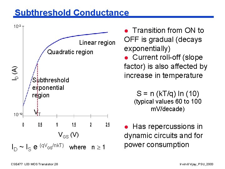
Subthreshold Conductance 10 -2 Linear region ID (A) Quadratic region 10 -12 Transition from ON to OFF is gradual (decays exponentially) l Current roll-off (slope factor) is also affected by increase in temperature l Subthreshold exponential region S = n (k. T/q) ln (10) (typical values 60 to 100 m. V/decade) VT Has repercussions in dynamic circuits and for power consumption l VGS (V) ID ~ IS e (q. VGS/nk. T) where n 1 CSE 477 L 03 MOS Transistor. 28 Irwin&Vijay, PSU, 2003

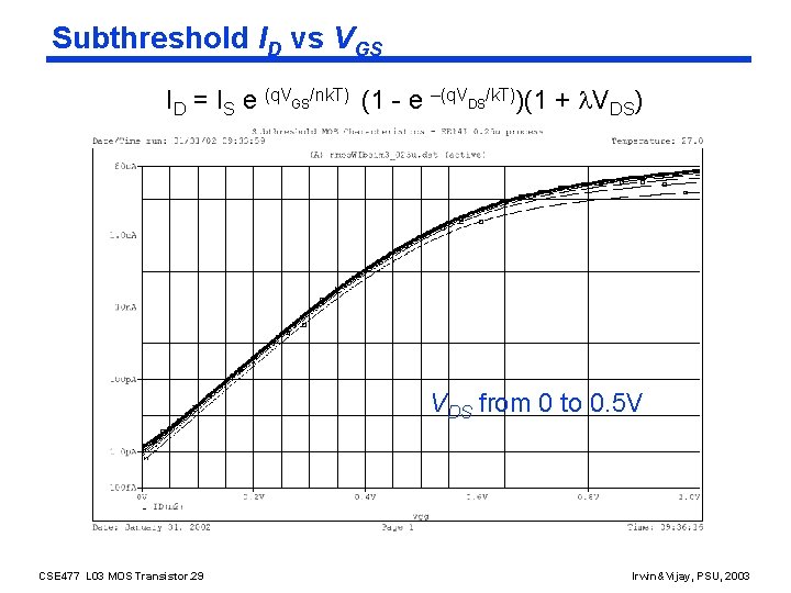
Subthreshold ID vs VGS ID = IS e (q. VGS/nk. T) (1 - e –(q. VDS/k. T))(1 + VDS) VDS from 0 to 0. 5 V CSE 477 L 03 MOS Transistor. 29 Irwin&Vijay, PSU, 2003

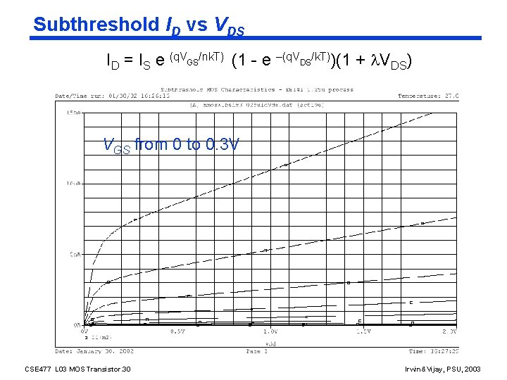
Subthreshold ID vs VDS ID = IS e (q. VGS/nk. T) (1 - e –(q. VDS/k. T))(1 + VDS) VGS from 0 to 0. 3 V CSE 477 L 03 MOS Transistor. 30 Irwin&Vijay, PSU, 2003

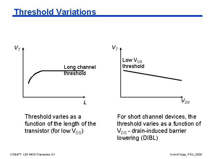
Threshold Variations VT VT Long channel threshold L Threshold varies as a function of the length of the transistor (for low VDS) CSE 477 L 03 MOS Transistor. 31 Low VDS threshold VDS For short channel devices, the threshold varies as a function of VDS - drain-induced barrier lowering (DIBL) Irwin&Vijay, PSU, 2003

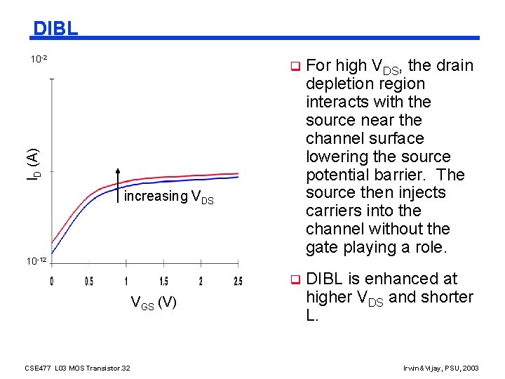
DIBL q For high VDS, the drain depletion region interacts with the source near the channel surface lowering the source potential barrier. The source then injects carriers into the channel without the gate playing a role. q DIBL is enhanced at higher VDS and shorter L. ID (A) 10 -2 increasing VDS 10 -12 VGS (V) CSE 477 L 03 MOS Transistor. 32 Irwin&Vijay, PSU, 2003

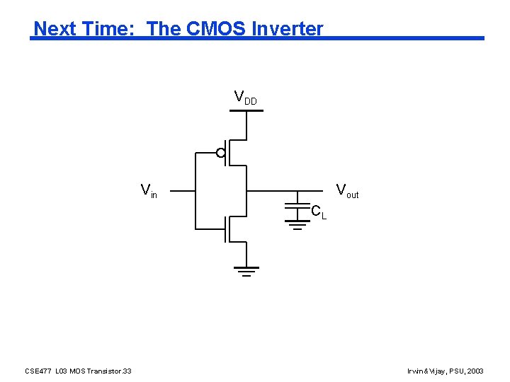
Next Time: The CMOS Inverter VDD Vin Vout CL CSE 477 L 03 MOS Transistor. 33 Irwin&Vijay, PSU, 2003

Next Lecture and Reminders q Next lecture l CMOS inverter – a static view - Reading assignment – Rabaey, et al, 5. 1 -5. 3 q Reminders l HW 1 due September 16 th (next class!) l Project team and title due September 18 th l Evening midterm exam scheduled - Monday, October 20 th , 20: 15 to 22: 15, Location TBD - Please let me know ASAP (via email) if you have a conflict CSE 477 L 03 MOS Transistor. 34 Irwin&Vijay, PSU, 2003