CSE 477 VLSI Digital Circuits Fall 2003 Lecture
- Slides: 20

CSE 477 VLSI Digital Circuits Fall 2003 Lecture 06: Static CMOS Logic Mary Jane Irwin ( www. cse. psu. edu/~mji ) www. cse. psu. edu/~cg 477 [Adapted from Rabaey’s Digital Integrated Circuits, Second Edition, © 2003 Rabaey, A. Chandrakasan, B. Nikolic] CSE 477 L 06 Static CMOS Logic. 1 J. Irwin&Vijay, PSU, 2003

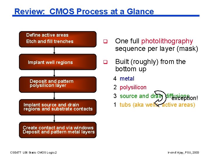
Review: CMOS Process at a Glance Define active areas Etch and fill trenches q One full photolithography sequence per layer (mask) Implant well regions q Built (roughly) from the bottom up Deposit and pattern polysilicon layer 4 metal 2 polysilicon 3 source and drain diffusions exception! Implant source and drain regions and substrate contacts 1 tubs (aka wells, active areas) Create contact and via windows Deposit and pattern metal layers CSE 477 L 06 Static CMOS Logic. 2 Irwin&Vijay, PSU, 2003

CMOS Circuit Styles q Static complementary CMOS - except during switching, output connected to either VDD or GND via a lowresistance path l high noise margins - full rail to rail swing - VOH and VOL are at VDD and GND, respectively l l q low output impedance, high input impedance no steady state path between VDD and GND (no static power consumption) delay a function of load capacitance and transistor resistance comparable rise and fall times (under the appropriate transistor sizing conditions) Dynamic CMOS - relies on temporary storage of signal values on the capacitance of high-impedance circuit nodes l l simpler, faster gates increased sensitivity to noise CSE 477 L 06 Static CMOS Logic. 3 Irwin&Vijay, PSU, 2003

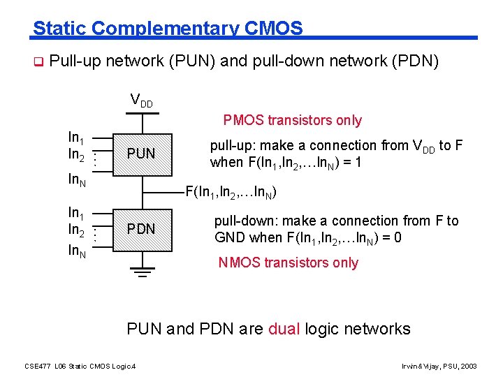
Static Complementary CMOS q Pull-up network (PUN) and pull-down network (PDN) VDD PMOS transistors only … In 1 In 2 PUN In. N F(In 1, In 2, …In. N) … In 1 In 2 In. N pull-up: make a connection from VDD to F when F(In 1, In 2, …In. N) = 1 PDN pull-down: make a connection from F to GND when F(In 1, In 2, …In. N) = 0 NMOS transistors only PUN and PDN are dual logic networks CSE 477 L 06 Static CMOS Logic. 4 Irwin&Vijay, PSU, 2003

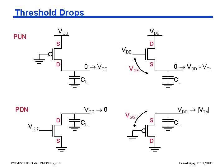
Threshold Drops VDD PUN VDD S D VDD 0 VDD VGS D S CL VDD 0 PDN VDD D S CSE 477 L 06 Static CMOS Logic. 6 CL 0 VDD - VTn CL VGS VDD |VTp| S CL D Irwin&Vijay, PSU, 2003

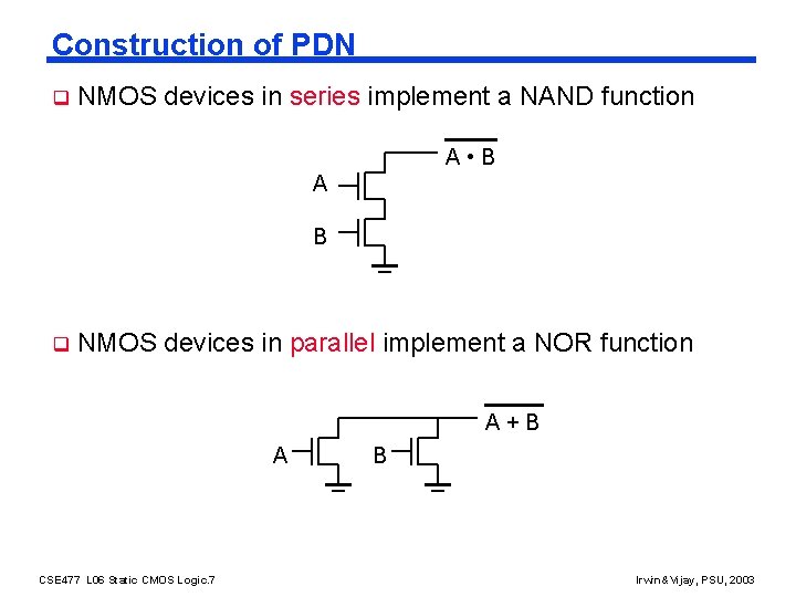
Construction of PDN q NMOS devices in series implement a NAND function A • B A B q NMOS devices in parallel implement a NOR function A+B A CSE 477 L 06 Static CMOS Logic. 7 B Irwin&Vijay, PSU, 2003

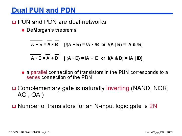
Dual PUN and PDN q PUN and PDN are dual networks l l De. Morgan’s theorems A+B=A • B [!(A + B) = !A • !B or !(A | B) = !A & !B] A • B=A+B [!(A • B) = !A + !B or !(A & B) = !A | !B] a parallel connection of transistors in the PUN corresponds to a series connection of the PDN q Complementary gate is naturally inverting (NAND, NOR, AOI, OAI) q Number of transistors for an N-input logic gate is 2 N CSE 477 L 06 Static CMOS Logic. 8 Irwin&Vijay, PSU, 2003

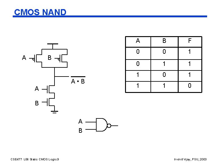
CMOS NAND A B A • B A A B F 0 0 1 1 1 0 B A B CSE 477 L 06 Static CMOS Logic. 9 Irwin&Vijay, PSU, 2003

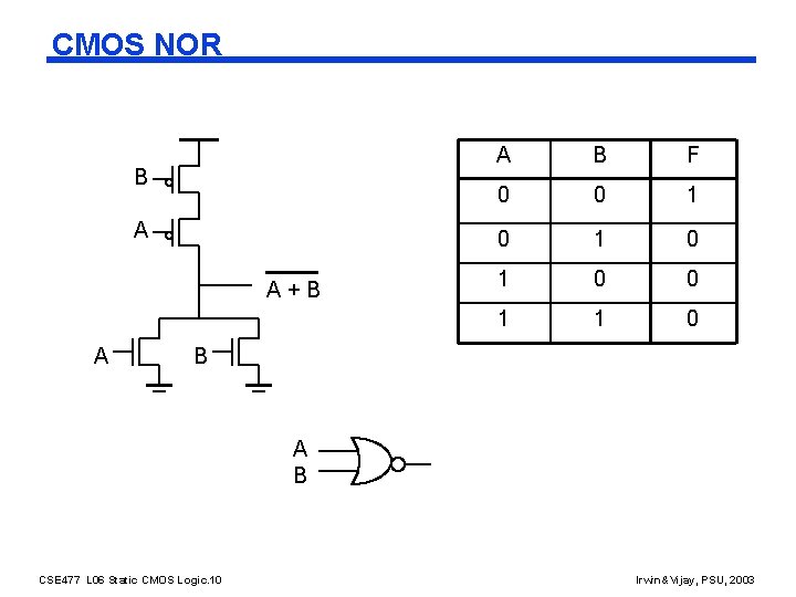
CMOS NOR B A A+B A A B F 0 0 1 0 1 0 0 1 1 0 B A B CSE 477 L 06 Static CMOS Logic. 10 Irwin&Vijay, PSU, 2003

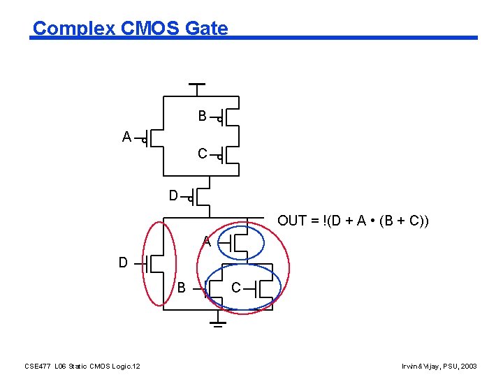
Complex CMOS Gate B A C D OUT = !(D + A • (B + C)) A D B CSE 477 L 06 Static CMOS Logic. 12 C Irwin&Vijay, PSU, 2003

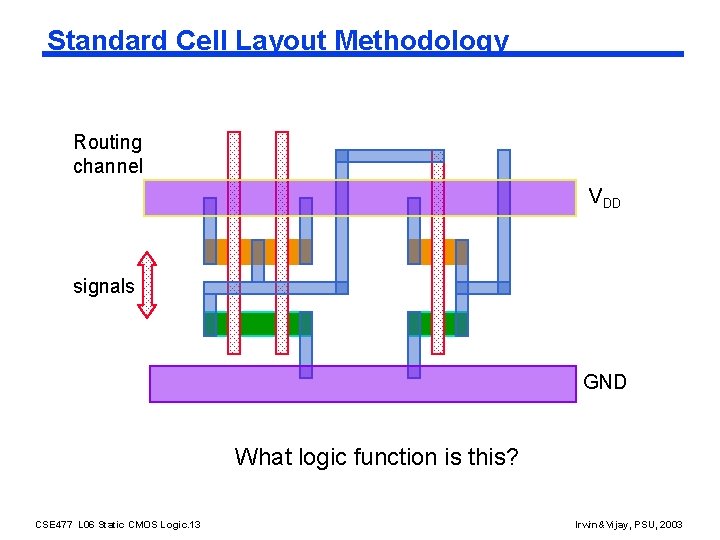
Standard Cell Layout Methodology Routing channel VDD signals GND What logic function is this? CSE 477 L 06 Static CMOS Logic. 13 Irwin&Vijay, PSU, 2003

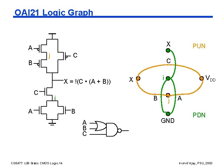
OAI 21 Logic Graph X A j C C B X = !(C • (A + B)) C i A i X B VDD j B A B C CSE 477 L 06 Static CMOS Logic. 14 PUN GND A PDN Irwin&Vijay, PSU, 2003

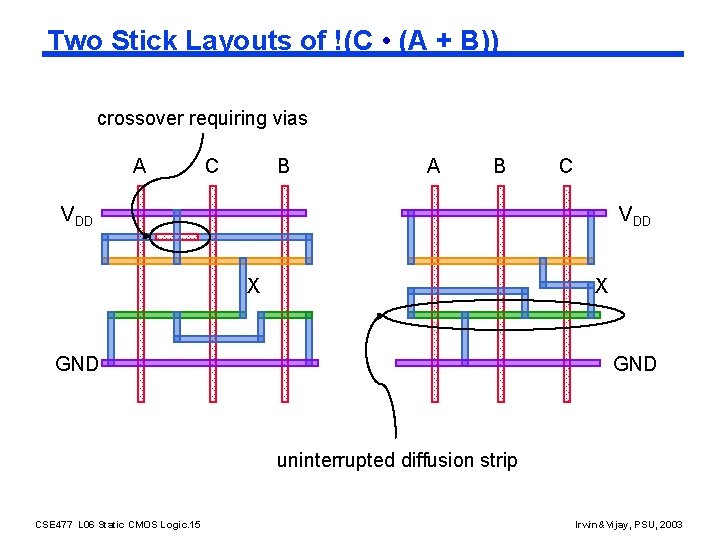
Two Stick Layouts of !(C • (A + B)) crossover requiring vias A C B A B C VDD X X GND uninterrupted diffusion strip CSE 477 L 06 Static CMOS Logic. 15 Irwin&Vijay, PSU, 2003

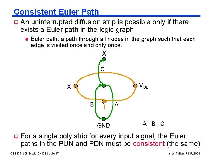
Consistent Euler Path q An uninterrupted diffusion strip is possible only if there exists a Euler path in the logic graph l Euler path: a path through all nodes in the graph such that each edge is visited once and only once. X C i X B VDD j GND q A A B C For a single poly strip for every input signal, the Euler paths in the PUN and PDN must be consistent (the same) CSE 477 L 06 Static CMOS Logic. 17 Irwin&Vijay, PSU, 2003

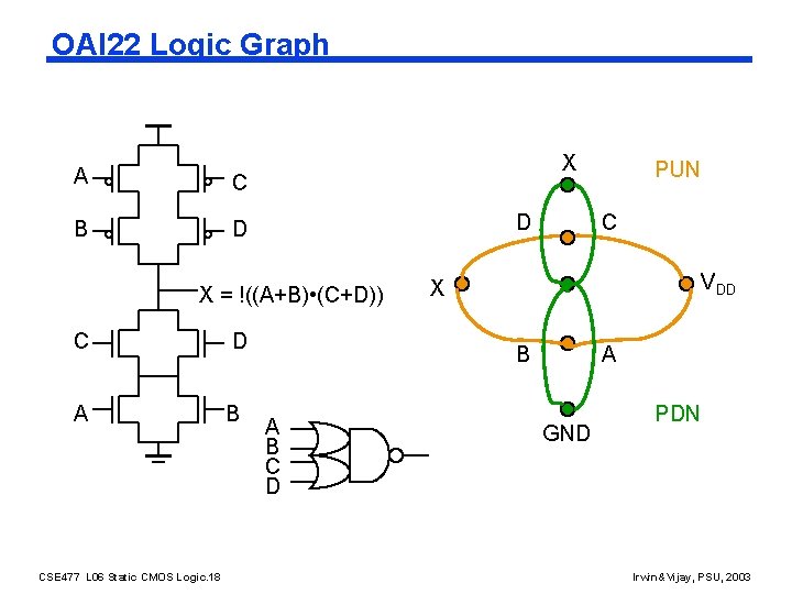
OAI 22 Logic Graph A C B D X = !((A+B) • (C+D)) C D A B CSE 477 L 06 Static CMOS Logic. 18 C VDD X B A B C D PUN A GND PDN Irwin&Vijay, PSU, 2003

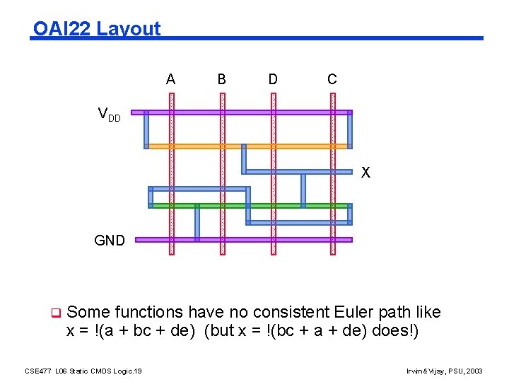
OAI 22 Layout A B D C VDD X GND q Some functions have no consistent Euler path like x = !(a + bc + de) (but x = !(bc + a + de) does!) CSE 477 L 06 Static CMOS Logic. 19 Irwin&Vijay, PSU, 2003

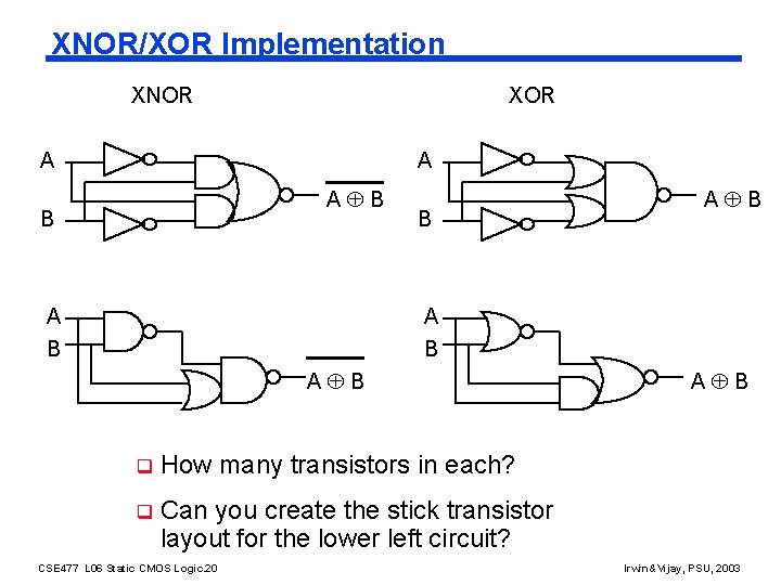
XNOR/XOR Implementation XNOR XOR A A A B B A B A B q How many transistors in each? q Can you create the stick transistor layout for the lower left circuit? CSE 477 L 06 Static CMOS Logic. 20 A B Irwin&Vijay, PSU, 2003

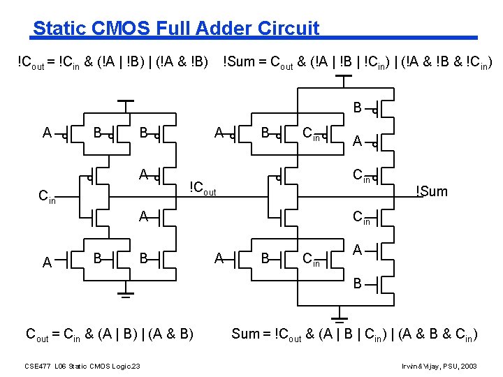
Static CMOS Full Adder Circuit !Cout = !Cin & (!A | !B) | (!A & !B) !Sum = Cout & (!A | !B | !Cin) | (!A & !B & !Cin) B A B B A Cin A B Cin !Cout A A B B A !Sum Cin A B Cout = Cin & (A | B) | (A & B) CSE 477 L 06 Static CMOS Logic. 23 Sum = !Cout & (A | B | Cin) | (A & B & Cin) Irwin&Vijay, PSU, 2003

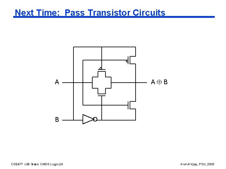
Next Time: Pass Transistor Circuits A A B B CSE 477 L 06 Static CMOS Logic. 24 Irwin&Vijay, PSU, 2003

Next Lecture and Reminders q Next lecture l Pass transistor logic - Reading assignment – Rabaey, et al, 6. 2. 3 presented by guest lecturer Greg Link q Reminders l l I will be out of town Wed through Friday (so no office hours Wednesday this week, sorry) HW#2 due September 30 th (next Tuesday) Project specs (on-line) due October 9 th Evening midterm exam scheduled - Monday, October 20 th , 20: 15 to 22: 15, Location TBD - Only one midterm conflict filed for so far CSE 477 L 06 Static CMOS Logic. 25 Irwin&Vijay, PSU, 2003