CSE 477 VLSI Digital Circuits Fall 2003 Lecture
- Slides: 28

CSE 477 VLSI Digital Circuits Fall 2003 Lecture 26: Low Power Techniques in Microarchitectures and Memories Mary Jane Irwin ( www. cse. psu. edu/~mji ) www. cse. psu. edu/~cg 477 [Adapted from Rabaey’s Digital Integrated Circuits, Second Edition, © 2003 Rabaey, A. Chandrakasan, B. Nikolic] CSE 477 L 26 System Power. 1 J. Irwin&Vijay, PSU, 2003

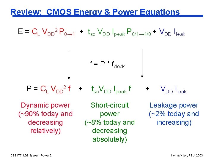
Review: CMOS Energy & Power Equations E = CL VDD 2 P 0 1 + tsc VDD Ipeak P 0/1 1/0 + VDD Ileak f = P * fclock P = CL VDD 2 f Dynamic power (~90% today and decreasing relatively) CSE 477 L 26 System Power. 2 + tsc. VDD Ipeak f Short-circuit power (~8% today and decreasing absolutely) + VDD Ileak Leakage power (~2% today and increasing) Irwin&Vijay, PSU, 2003

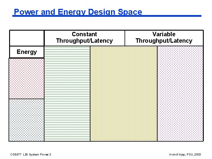
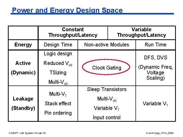
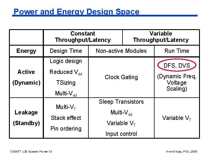
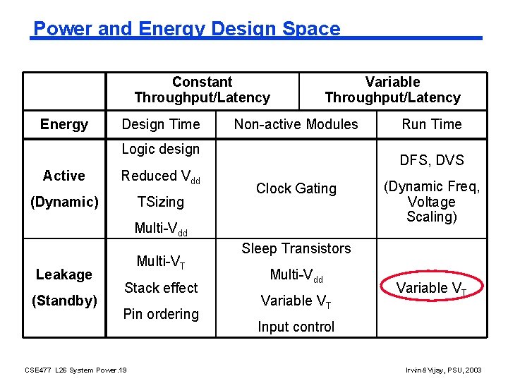
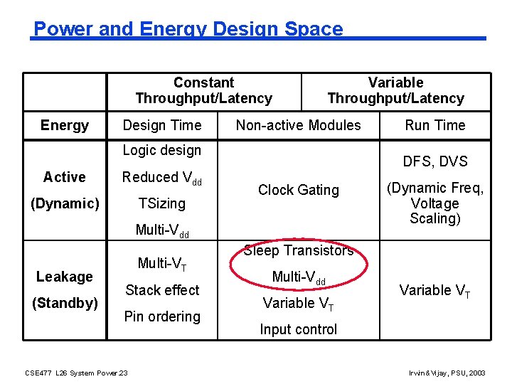
Power and Energy Design Space Constant Throughput/Latency Energy Design Time Variable Throughput/Latency Non-active Modules Logic design Active Reduced Vdd (Dynamic) TSizing DFS, DVS Clock Gating Multi-Vdd Leakage (Standby) CSE 477 L 26 System Power. 3 Multi-VT Stack effect Pin ordering Run Time (Dynamic Freq, Voltage Scaling) Sleep Transistors Multi-Vdd Variable VT Input control Irwin&Vijay, PSU, 2003

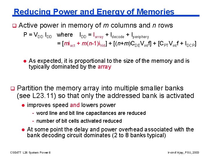
Reducing Power and Energy of Memories q Active power in memory of m columns and n rows P = VDD IDD where IDD = Iarray + Idecode + Iperiphery = [miact + m(n-1)ihld] + [(n+m)CDEVintf] + [CPTVintf + IDCP] l q As expected, it is proportional to the size of the memory and is typically dominated by the array Partition the memory array into multiple smaller banks (see L 23. 11) so that only the addressed bank is activated l improves speed and lowers power - word line and bit line capacitances are reduced - number of bit cells activated reduced l At some point the delay and power overhead associated with the bank decoding circuit dominates (2 to 8 banks typical) CSE 477 L 26 System Power. 6 Irwin&Vijay, PSU, 2003

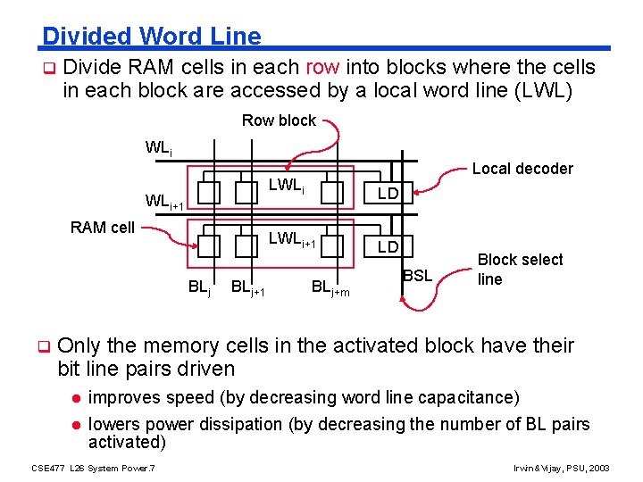
Divided Word Line q Divide RAM cells in each row into blocks where the cells in each block are accessed by a local word line (LWL) Row block WLi+1 RAM cell BLj q BLj+1 Local decoder LWLi LD LWLi+1 LD BLj+m BSL Block select line Only the memory cells in the activated block have their bit line pairs driven l l improves speed (by decreasing word line capacitance) lowers power dissipation (by decreasing the number of BL pairs activated) CSE 477 L 26 System Power. 7 Irwin&Vijay, PSU, 2003

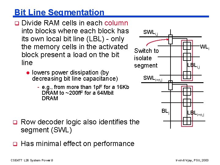
Bit Line Segmentation q Divide RAM cells in each column into blocks where each block has SWLi, j its own local bit line (LBL) - only the memory cells in the activated Switch to block present a load on the bit isolate line segment l lowers power dissipation (by decreasing bit line capacitance) WLi LBLi, j SWLi+n, j - e. g. , from more than 1 p. F for a 16 Kb DRAM to ~200 f. F for a 64 Mbit DRAM BLj q Row decoder logic also identifies the segment (SWL) q Has minimal effect on performance CSE 477 L 26 System Power. 8 LBLi+n, j Irwin&Vijay, PSU, 2003

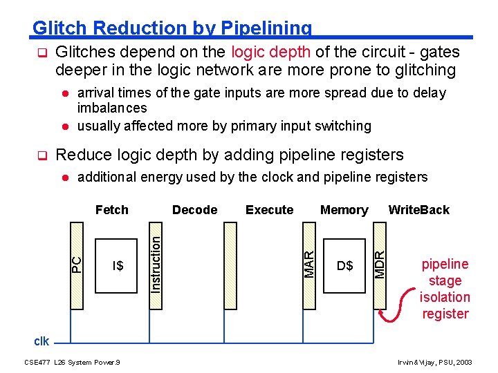
Glitch Reduction by Pipelining Glitches depend on the logic depth of the circuit - gates deeper in the logic network are more prone to glitching l l Reduce logic depth by adding pipeline registers l additional energy used by the clock and pipeline registers I$ Decode Instruction PC Fetch Execute Memory D$ Write. Back MDR q arrival times of the gate inputs are more spread due to delay imbalances usually affected more by primary input switching MAR q pipeline stage isolation register clk CSE 477 L 26 System Power. 9 Irwin&Vijay, PSU, 2003

Power and Energy Design Space Constant Throughput/Latency Energy Design Time Variable Throughput/Latency Non-active Modules Logic design Active Reduced Vdd (Dynamic) TSizing DFS, DVS Clock Gating Multi-Vdd Leakage (Standby) Multi-VT Stack effect Pin ordering CSE 477 L 26 System Power. 10 Run Time (Dynamic Freq, Voltage Scaling) Sleep Transistors Multi-Vdd Variable VT Input control Irwin&Vijay, PSU, 2003

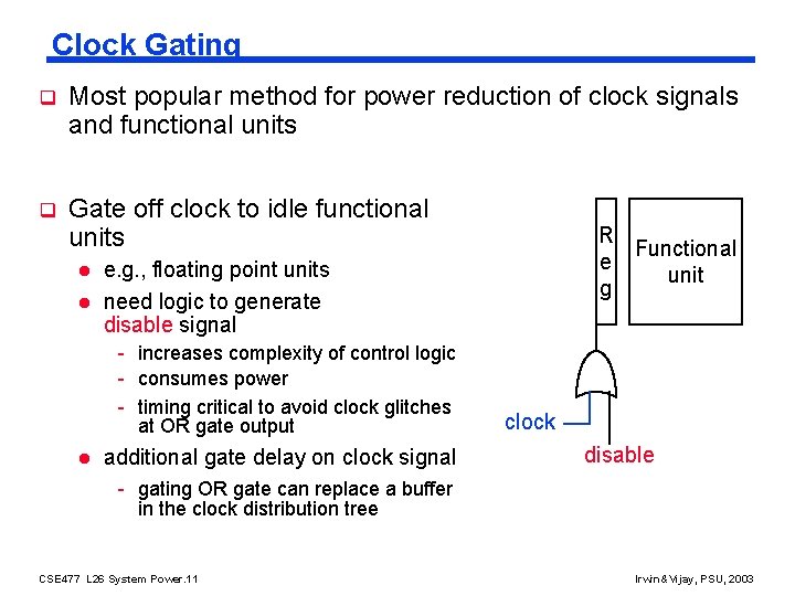
Clock Gating q Most popular method for power reduction of clock signals and functional units q Gate off clock to idle functional units l l e. g. , floating point units need logic to generate disable signal - increases complexity of control logic - consumes power - timing critical to avoid clock glitches at OR gate output l R Functional e unit g additional gate delay on clock signal clock disable - gating OR gate can replace a buffer in the clock distribution tree CSE 477 L 26 System Power. 11 Irwin&Vijay, PSU, 2003

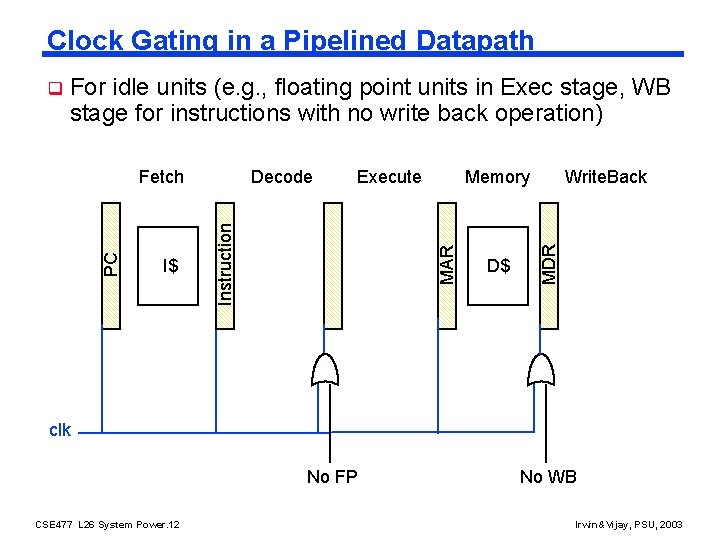
Clock Gating in a Pipelined Datapath For idle units (e. g. , floating point units in Exec stage, WB stage for instructions with no write back operation) Execute Memory D$ Write. Back MDR I$ Decode Instruction PC Fetch MAR q clk No FP CSE 477 L 26 System Power. 12 No WB Irwin&Vijay, PSU, 2003

Power and Energy Design Space Constant Throughput/Latency Energy Design Time Variable Throughput/Latency Non-active Modules Logic design Active Reduced Vdd (Dynamic) TSizing DFS, DVS Clock Gating Multi-Vdd Leakage (Standby) Multi-VT Stack effect Pin ordering CSE 477 L 26 System Power. 13 Run Time (Dynamic Freq, Voltage Scaling) Sleep Transistors Multi-Vdd Variable VT Input control Irwin&Vijay, PSU, 2003

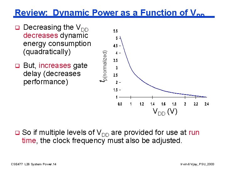
q Decreasing the VDD decreases dynamic energy consumption (quadratically) q But, increases gate delay (decreases performance) tp(normalized) Review: Dynamic Power as a Function of VDD (V) q So if multiple levels of VDD are provided for use at run time, the clock frequency must also be adjusted. CSE 477 L 26 System Power. 14 Irwin&Vijay, PSU, 2003

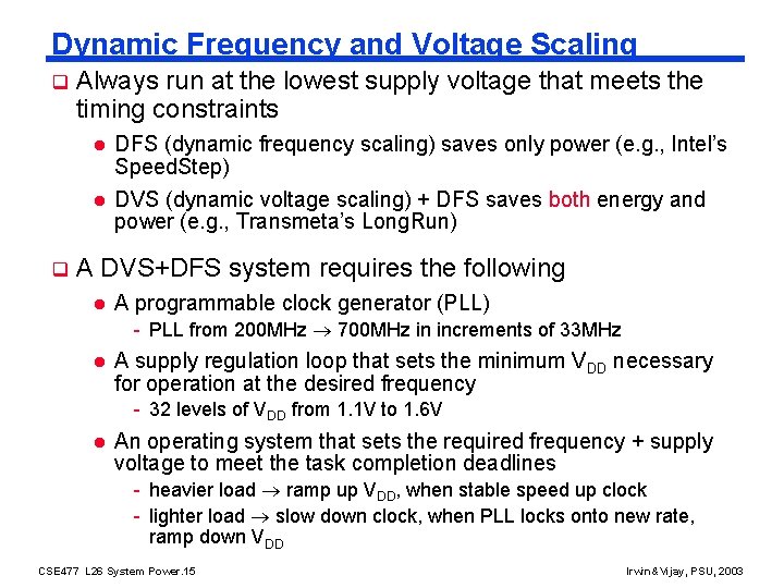
Dynamic Frequency and Voltage Scaling q q Always run at the lowest supply voltage that meets the timing constraints l DFS (dynamic frequency scaling) saves only power (e. g. , Intel’s Speed. Step) l DVS (dynamic voltage scaling) + DFS saves both energy and power (e. g. , Transmeta’s Long. Run) A DVS+DFS system requires the following l A programmable clock generator (PLL) - PLL from 200 MHz 700 MHz in increments of 33 MHz l A supply regulation loop that sets the minimum VDD necessary for operation at the desired frequency - 32 levels of VDD from 1. 1 V to 1. 6 V l An operating system that sets the required frequency + supply voltage to meet the task completion deadlines - heavier load ramp up VDD, when stable speed up clock - lighter load slow down clock, when PLL locks onto new rate, ramp down VDD CSE 477 L 26 System Power. 15 Irwin&Vijay, PSU, 2003

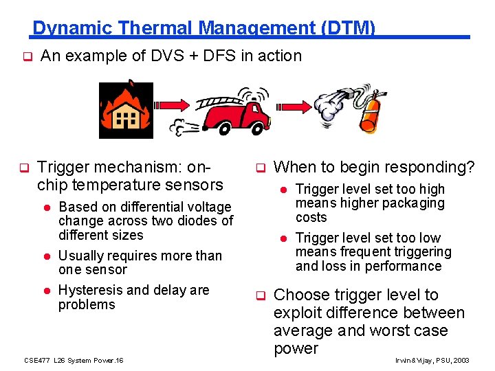
Dynamic Thermal Management (DTM) q An example of DVS + DFS in action q Trigger mechanism: onchip temperature sensors l q l Based on differential voltage change across two diodes of different sizes l Usually requires more than one sensor l Hysteresis and delay are problems CSE 477 L 26 System Power. 16 When to begin responding? l q Trigger level set too high means higher packaging costs Trigger level set too low means frequent triggering and loss in performance Choose trigger level to exploit difference between average and worst case power Irwin&Vijay, PSU, 2003

DTM Initiation and Response Mechanisms q Operating system or micro-architectural initiation mechanism? l q q Hardware support can reduce the performance penalty by 20 -30% Response mechanism – DVS+DFS l Incurs some delay since there is a OS context switch needed to set the new level of DVS + DFS l Increasing the trigger level reduces the frequency of context switching to set DVS + DFS The use of a thermal window (100 Kcycles+) can help to “smooth” short thermal spikes CSE 477 L 26 System Power. 17 Irwin&Vijay, PSU, 2003

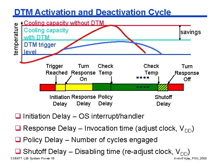
temperature DTM Activation and Deactivation Cycle Cooling capacity without DTM Cooling capacity with DTM trigger level Turn Check Trigger Reached Response Temp On savings Check Temp Initiation Response Policy Delay Turn Response Off Shutoff Delay q Initiation Delay – OS interrupt/handler q Response Delay – Invocation time (adjust clock, VDD) q Policy Delay – Number of cycles engaged q Shutoff Delay – Disabling time (re-adjust clock, VDD) CSE 477 L 26 System Power. 18 Irwin&Vijay, PSU, 2003

Power and Energy Design Space Constant Throughput/Latency Energy Design Time Variable Throughput/Latency Non-active Modules Logic design Active Reduced Vdd (Dynamic) TSizing DFS, DVS Clock Gating Multi-Vdd Leakage (Standby) Multi-VT Stack effect Pin ordering CSE 477 L 26 System Power. 19 Run Time (Dynamic Freq, Voltage Scaling) Sleep Transistors Multi-Vdd Variable VT Input control Irwin&Vijay, PSU, 2003

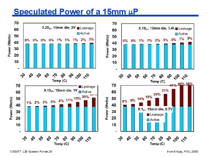
Speculated Power of a 15 mm m. P CSE 477 L 26 System Power. 20 Irwin&Vijay, PSU, 2003

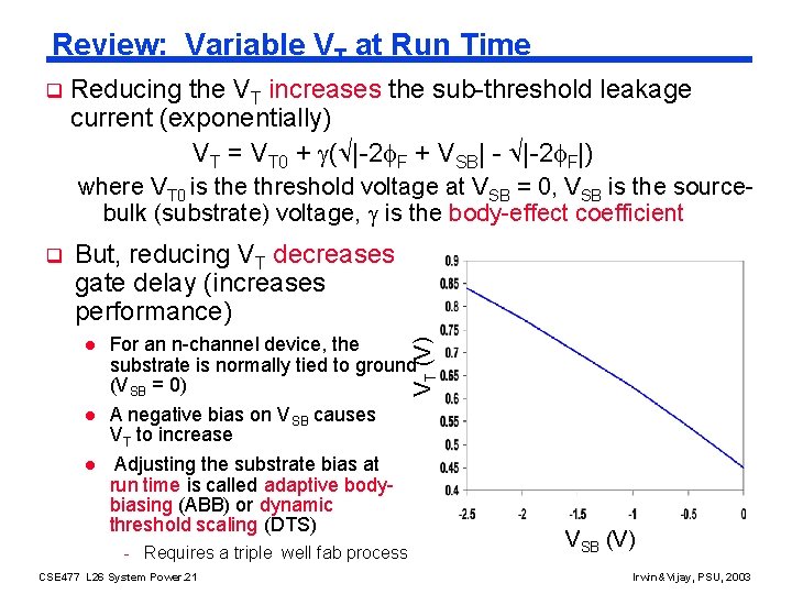
Review: Variable VT at Run Time q Reducing the VT increases the sub-threshold leakage current (exponentially) VT = VT 0 + ( |-2 F + VSB| - |-2 F|) where VT 0 is the threshold voltage at VSB = 0, VSB is the sourcebulk (substrate) voltage, is the body-effect coefficient But, reducing VT decreases gate delay (increases performance) l l l For an n-channel device, the substrate is normally tied to ground (VSB = 0) A negative bias on VSB causes VT to increase Adjusting the substrate bias at run time is called adaptive bodybiasing (ABB) or dynamic threshold scaling (DTS) VT (V) q - Requires a triple well fab process CSE 477 L 26 System Power. 21 VSB (V) Irwin&Vijay, PSU, 2003

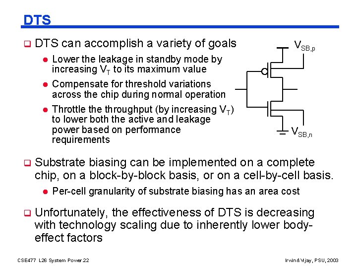
DTS q DTS can accomplish a variety of goals l l l q Lower the leakage in standby mode by increasing VT to its maximum value Compensate for threshold variations across the chip during normal operation Throttle throughput (by increasing VT) to lower both the active and leakage power based on performance requirements VSB, n Substrate biasing can be implemented on a complete chip, on a block-by-block basis, or on a cell-by-cell basis. l q VSB, p Per-cell granularity of substrate biasing has an area cost Unfortunately, the effectiveness of DTS is decreasing with technology scaling due to inherently lower bodyeffect factors CSE 477 L 26 System Power. 22 Irwin&Vijay, PSU, 2003

Power and Energy Design Space Constant Throughput/Latency Energy Design Time Variable Throughput/Latency Non-active Modules Logic design Active Reduced Vdd (Dynamic) TSizing DFS, DVS Clock Gating Multi-Vdd Leakage (Standby) Multi-VT Stack effect Pin ordering CSE 477 L 26 System Power. 23 Run Time (Dynamic Freq, Voltage Scaling) Sleep Transistors Multi-Vdd Variable VT Input control Irwin&Vijay, PSU, 2003

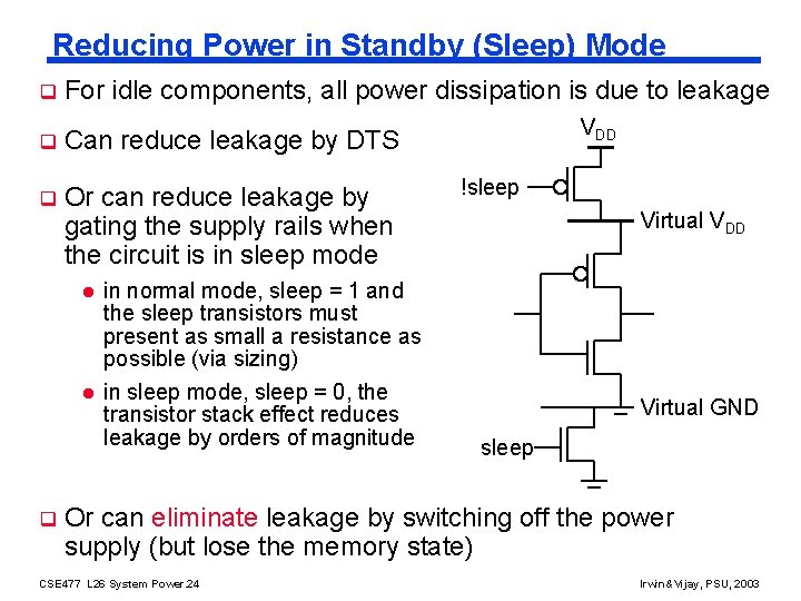
Reducing Power in Standby (Sleep) Mode q For idle components, all power dissipation is due to leakage q Can reduce leakage by DTS q Or can reduce leakage by gating the supply rails when the circuit is in sleep mode q l in normal mode, sleep = 1 and the sleep transistors must present as small a resistance as possible (via sizing) l in sleep mode, sleep = 0, the transistor stack effect reduces leakage by orders of magnitude VDD !sleep Virtual VDD Virtual GND sleep Or can eliminate leakage by switching off the power supply (but lose the memory state) CSE 477 L 26 System Power. 24 Irwin&Vijay, PSU, 2003

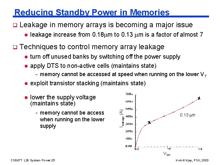
Reducing Standby Power in Memories q Leakage in memory arrays is becoming a major issue l q leakage increase from 0. 18 m to 0. 13 m is a factor of almost 7 Techniques to control memory array leakage l l turn off unused banks by switching off the power supply apply DTS to non-active cells (maintains state) - memory cannot be accessed at speed when running on the lower VT exploit transistor stacking (maintains state) l lower the supply voltage (maintains state) - memory cannot be access when running on the lower supply Ileakage (A) l 0. 13 m VDD CSE 477 L 26 System Power. 25 Irwin&Vijay, PSU, 2003

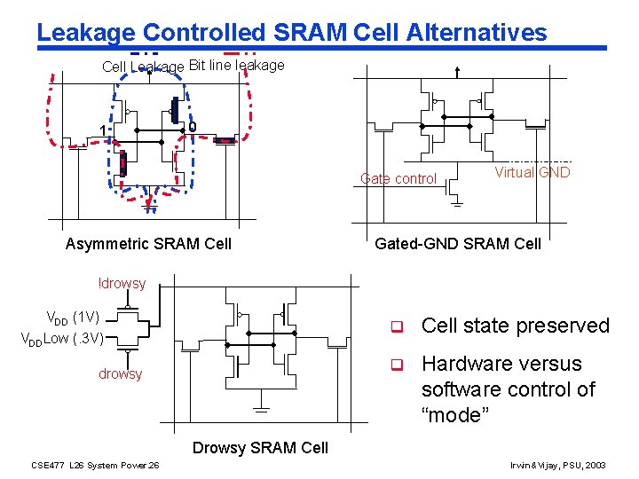
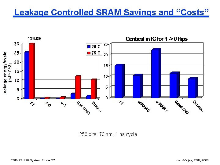
Leakage Controlled SRAM Cell Alternatives Cell Leakage Bit line leakage 1 0 Gate control Asymmetric SRAM Cell Virtual GND Gated-GND SRAM Cell !drowsy VDD (1 V) VDDLow (. 3 V) drowsy q Cell state preserved q Hardware versus software control of “mode” Drowsy SRAM Cell CSE 477 L 26 System Power. 26 Irwin&Vijay, PSU, 2003

Leakage Controlled SRAM Savings and “Costs” 134. 09 256 bits, 70 nm, 1 ns cycle CSE 477 L 26 System Power. 27 Irwin&Vijay, PSU, 2003

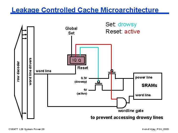
Leakage Controlled Cache Microarchitecture word line drivers row decoder Global Set: drowsy Reset: active !Q Q word line Reset 0. 3 V (drowsy) 1 V (active) power line SRAMs word line wordline gate to prevent accessing drowsy lines CSE 477 L 26 System Power. 28 Irwin&Vijay, PSU, 2003

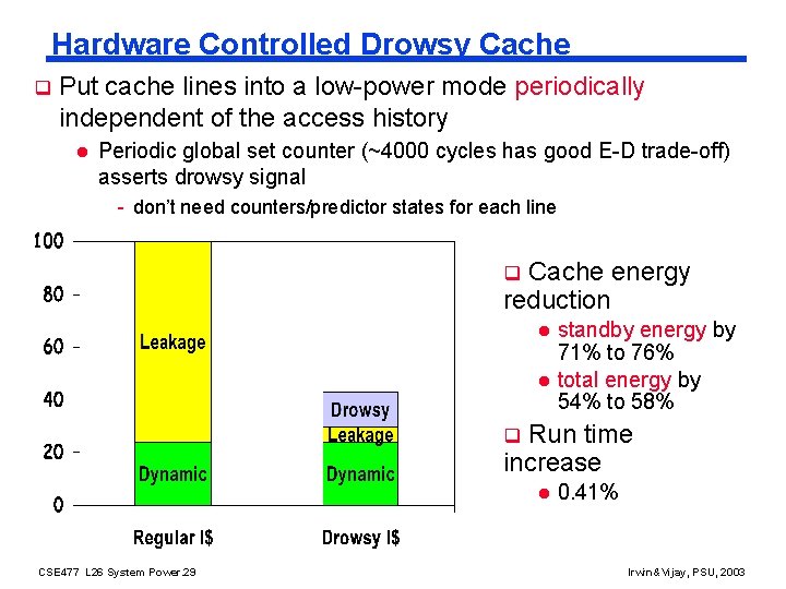
Hardware Controlled Drowsy Cache q Put cache lines into a low-power mode periodically independent of the access history l Periodic global set counter (~4000 cycles has good E-D trade-off) asserts drowsy signal - don’t need counters/predictor states for each line Cache energy reduction q l l standby energy by 71% to 76% total energy by 54% to 58% Run time increase q l CSE 477 L 26 System Power. 29 0. 41% Irwin&Vijay, PSU, 2003

Next Lecture and Reminders q Next lecture l System level interconnect - Reading assignment – Rabaey, et al, Chapter 9 q Reminders l Project final reports due on-line by 5: 00 pm on Friday, December 5 th l Final grading negotiations/correction (except for the final exam) must be concluded by December 10 th l Final exam scheduled - Tuesday, December 16 th from 10: 10 to noon in 118 and 113 Thomas CSE 477 L 26 System Power. 30 Irwin&Vijay, PSU, 2003