CSE 477 VLSI Digital Circuits Fall 2003 Lecture
- Slides: 16

CSE 477 VLSI Digital Circuits Fall 2003 Lecture 27: System Level Interconnect Mary Jane Irwin ( www. cse. psu. edu/~mji ) www. cse. psu. edu/~cg 477 [Adapted from Rabaey’s Digital Integrated Circuits, Second Edition, © 2003 Rabaey, A. Chandrakasan, B. Nikolic] CSE 477 L 27 System Interconnect. 1 J. Irwin&Vijay, PSU, 2003

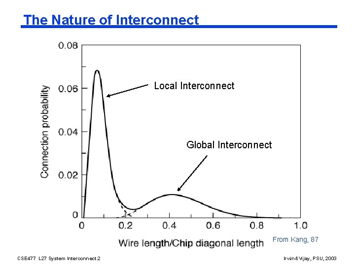
The Nature of Interconnect Local Interconnect Global Interconnect From Kang, 87 CSE 477 L 27 System Interconnect. 2 Irwin&Vijay, PSU, 2003

Global Interconnect q Classes of global interconnects l System level signal interconnect - buses Global set and reset lines System clock(s) l VDD and GND planes l l q q Classes of parasitics l capacitive l resistive l inductive Impacts of parasitics l l Reduced reliability (crosstalk) Reduced performance CSE 477 L 27 System Interconnect. 3 Irwin&Vijay, PSU, 2003

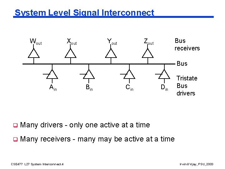
System Level Signal Interconnect Wout Xout Yout Bus receivers Zout Bus Ain Bin Cin Din q Many drivers - only one active at a time q Many receivers - many may be active at a time CSE 477 L 27 System Interconnect. 4 Tristate Bus drivers Irwin&Vijay, PSU, 2003

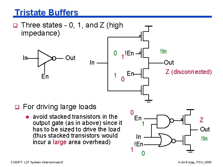
Tristate Buffers q Three states - 0, 1, and Z (high impedance) In Out 0 In En q 1 1 0 For driving large loads l avoid stacked transistors in the output gate (as in above) since it has to be sized to drive the load (thus stacked transistors would incur a large area overhead) Out Z (disconnected) En 0 1 CSE 477 L 27 System Interconnect. 6 !In !En En 1 In !En Z Out !In 0 Irwin&Vijay, PSU, 2003

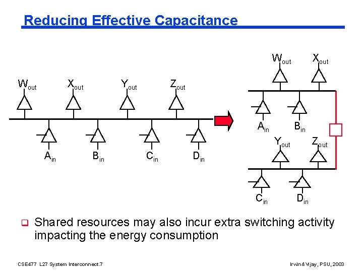
Reducing Effective Capacitance Wout Xout Yout Xout Zout Ain Bin Yout Ain Bin Cin Din Cin q Zout Din Shared resources may also incur extra switching activity impacting the energy consumption CSE 477 L 27 System Interconnect. 7 Irwin&Vijay, PSU, 2003

Driving Large Capacitive Loads q Large fan out on-chip loads can be in the multi-picofarad range; off-chip loads can be as large as 50 p. F q Design techniques for driving large loads l Appropriately sized transistors in the driving gate l Partitioning drivers into chains of gradually increasing (in size) buffers - when optimizing for performance, the delay of a multi-stage driver should be divided equally over all stages - a fan-out (sizing) factor of 4 (FA 4) per stage leads to the minimum delay for contemporary processes l l Use better interconnect materials (like copper and low-K dielectrics) Introduce buffers (buffer (or repeater) insertion) into long wires to reduce the propagation delay CSE 477 L 27 System Interconnect. 8 Irwin&Vijay, PSU, 2003

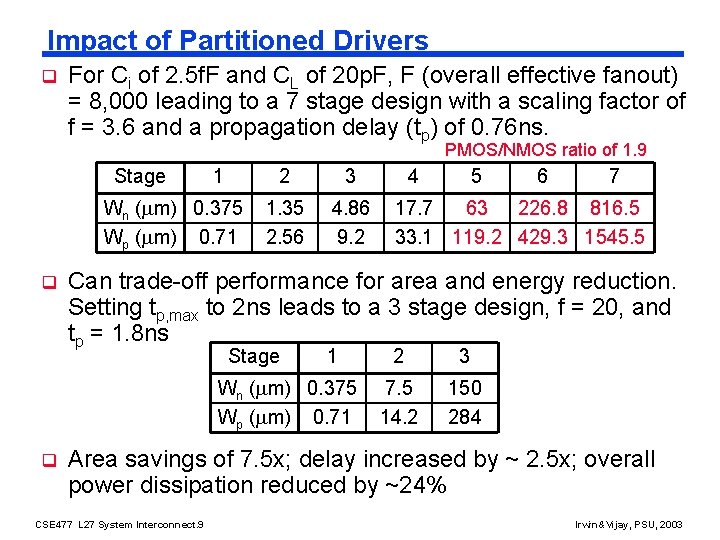
Impact of Partitioned Drivers q For Ci of 2. 5 f. F and CL of 20 p. F, F (overall effective fanout) = 8, 000 leading to a 7 stage design with a scaling factor of f = 3. 6 and a propagation delay (tp) of 0. 76 ns. PMOS/NMOS ratio of 1. 9 Stage 1 Wn ( m) 0. 375 Wp ( m) 0. 71 q 2 3 1. 35 2. 56 4. 86 9. 2 5 6 7 17. 7 63 226. 8 816. 5 33. 1 119. 2 429. 3 1545. 5 Can trade-off performance for area and energy reduction. Setting tp, max to 2 ns leads to a 3 stage design, f = 20, and tp = 1. 8 ns Stage 1 Wn ( m) 0. 375 Wp ( m) 0. 71 q 4 2 3 7. 5 14. 2 150 284 Area savings of 7. 5 x; delay increased by ~ 2. 5 x; overall power dissipation reduced by ~24% CSE 477 L 27 System Interconnect. 9 Irwin&Vijay, PSU, 2003

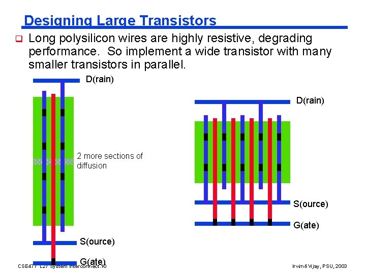
Designing Large Transistors q Long polysilicon wires are highly resistive, degrading performance. So implement a wide transistor with many smaller transistors in parallel. D(rain) 2 more sections of diffusion S(ource) G(ate) CSE 477 L 27 System Interconnect. 10 Irwin&Vijay, PSU, 2003

Impact of Better Interconnect Materials q Use better interconnect materials l As processes shrink, wires get shorter (reducing C) but they get closer together (increasing C) and narrower (increasing R). So RC wire delay increases and capacitive coupling gets worse. - Copper has about 40% lower resistivity than aluminum, so copper wires can be thinner (reducing C) without increasing R l Use silicides (WSi 2, Ti. Si 2, Pt. Si 2 and Ta. Si) - Conductivity is 8 -10 times better than poly alone l Low capacitance (low-k) dielectrics (insulators) such as polymide or even air instead of Si. O 2 - must also be suitable thermally and mechanically compatible with (copper) interconnect q Only buys one generation! q Drive long poly wires from both ends – or use extra metal bypass wires l providing a bypass line every 16 cells for a poly word line driving 1024 cells in a memory core reduces the WL delay by ~4, 000 CSE 477 L 27 System Interconnect. 11 Irwin&Vijay, PSU, 2003

Impact of Buffer Insertion q The most popular design approach to reducing the propagation delay of long wires is to introduce intermediate buffers (repeaters) in the interconnect line. l making a wire m times shorter reduces its propagation delay quadratically and is sufficient to offset the extra delay of the repeaters (tpbuf) when the wire is sufficiently long mopt = L ((0. 38 rc)/tpbuf) = (tpwireunbuffered/tpbuf) tp, opt = 2 (tpwireunbuffered tpbuf) q For example, for a 10 cm long, 1 m wide wire and a tpbuf of 0. 1 ns, partitioning a AL 1 wire into 18 sections would give an overall delay time of 3. 5 ns (compared to the unbuffered delay of 32. 4 ns). For poly the delay reduces to 212 ns (from 112 s) with 1, 058 sections and for AL 5 to 1. 3 ns (from 4. 2 ns) with 6 sections Repeater insertion is an essential tool in combating long wire delays CSE 477 L 27 System Interconnect. 12 Irwin&Vijay, PSU, 2003 q

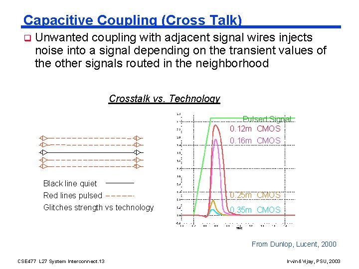
Capacitive Coupling (Cross Talk) q Unwanted coupling with adjacent signal wires injects noise into a signal depending on the transient values of the other signals routed in the neighborhood Crosstalk vs. Technology Pulsed Signal 0. 12 m CMOS 0. 16 m CMOS Black line quiet Red lines pulsed 0. 25 m CMOS Glitches strength vs technology 0. 35 m CMOS From Dunlop, Lucent, 2000 CSE 477 L 27 System Interconnect. 13 Irwin&Vijay, PSU, 2003

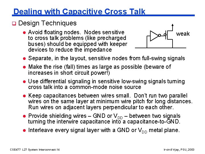
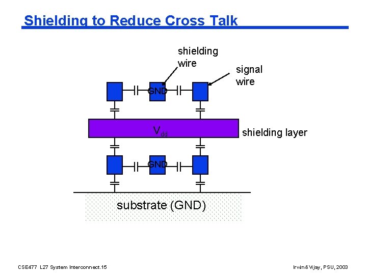
Dealing with Capacitive Cross Talk q Design Techniques l Avoid floating nodes. Nodes sensitive to cross talk problems (like precharged buses) should be equipped with keeper devices to reduce the impedance l Separate, in the layout, sensitive nodes from full-swing signals l Make the rise (fall) times as large as possible (beware of increases in short circuit power!) l Use differential signaling in sensitive low-swing signals turning cross talk into a common-mode noise source Keep capacitances between wires small. Don’t run two parallel wires on the same layer at minimum wire pitch for long distances. Run wires on adjacent layers perpendicular to each other. Provide shielding wires – GND or VDD – between two signals turning the interwire capacitance into a capacitance-to-GND. Interleave every signal layer with a GND or VDD metal plane. l l l CSE 477 L 27 System Interconnect. 14 weak Irwin&Vijay, PSU, 2003

Shielding to Reduce Cross Talk shielding wire GND Vdd signal wire shielding layer GND substrate (GND) CSE 477 L 27 System Interconnect. 15 Irwin&Vijay, PSU, 2003

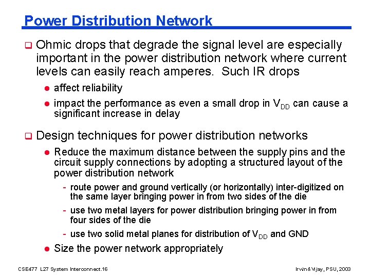
Power Distribution Network q q Ohmic drops that degrade the signal level are especially important in the power distribution network where current levels can easily reach amperes. Such IR drops l affect reliability l impact the performance as even a small drop in VDD can cause a significant increase in delay Design techniques for power distribution networks l Reduce the maximum distance between the supply pins and the circuit supply connections by adopting a structured layout of the power distribution network - route power and ground vertically (or horizontally) inter-digitized on the same layer bringing power in from two sides of the die - use two metal layers for power distribution bringing power in from four sides of the die - use two solid metal planes for distribution of VDD and GND l Size the power network appropriately CSE 477 L 27 System Interconnect. 16 Irwin&Vijay, PSU, 2003

Next Lecture and Reminders q Next (!last!) lecture l Design for test – for your reference only - Reading assignment – Rabaey, et al, Design Insert H. 1 -H. 4 l Technology trends and scaling – Greg will guest lecture - Reading assignment – Rabaey, et al, 2. 5; 3. 5; 4. 6; 5. 6 q Reminders l l Final grading negotiations/correction (except for the project prototype/final and the final exam) must be concluded by tomorrow, December 10 th Final exam scheduled - Tuesday, December 16 th from 10: 10 to noon in 118 and 113 Thomas CSE 477 L 27 System Interconnect. 17 Irwin&Vijay, PSU, 2003