CSE 477 VLSI Digital Circuits Fall 2003 Lecture

- Slides: 30

CSE 477 VLSI Digital Circuits Fall 2003 Lecture 11: Designing for Speed Mary Jane Irwin ( www. cse. psu. edu/~mji ) www. cse. psu. edu/~cg 477 [Adapted from Rabaey’s Digital Integrated Circuits, Second Edition, © 2003 Rabaey, A. Chandrakasan, B. Nikolic] CSE 477 L 11 Fast Logic. 1 J. Irwin&Vijay, PSU, 2003

Cray was a legend in computers … said that he liked to hire inexperienced engineers right out of school, because they do not usually know what’s supposed to be impossible. The Soul of a New Machine, Kidder, pg. 77 CSE 477 L 11 Fast Logic. 2 Irwin&Vijay, PSU, 2003

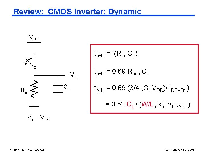
Review: CMOS Inverter: Dynamic VDD tp. HL = f(Rn, CL) Vout CL Rn tp. HL = 0. 69 Reqn CL tp. HL = 0. 69 (3/4 (CL VDD)/ IDSATn ) = 0. 52 CL / (W/Ln k’n VDSATn ) Vin = V DD CSE 477 L 11 Fast Logic. 3 Irwin&Vijay, PSU, 2003

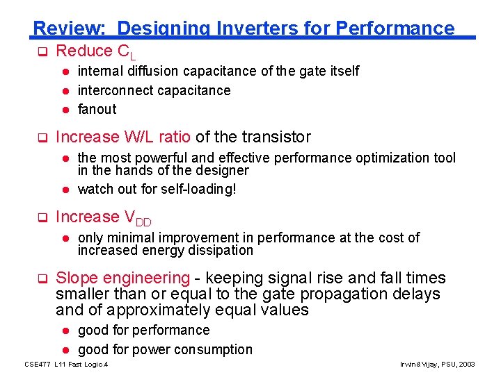
Review: Designing Inverters for Performance q Reduce CL l l l q Increase W/L ratio of the transistor l l q the most powerful and effective performance optimization tool in the hands of the designer watch out for self-loading! Increase VDD l q internal diffusion capacitance of the gate itself interconnect capacitance fanout only minimal improvement in performance at the cost of increased energy dissipation Slope engineering - keeping signal rise and fall times smaller than or equal to the gate propagation delays and of approximately equal values l l good for performance good for power consumption CSE 477 L 11 Fast Logic. 4 Irwin&Vijay, PSU, 2003

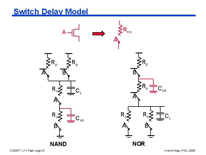
Switch Delay Model Req A A Rp Rp B B Rn Rp CL A A Rn B NAND CSE 477 L 11 Fast Logic. 5 Cint Rn Rn A B CL NOR Irwin&Vijay, PSU, 2003

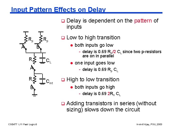
Input Pattern Effects on Delay Rp A Rp q Delay is dependent on the pattern of inputs q Low to high transition l B Rn - delay is 0. 69 Rp/2 CL since two p-resistors are on in parallel CL l A Rn B both inputs go low one input goes low - delay is 0. 69 Rp CL Cint q High to low transition l both inputs go high - delay is 0. 69 2 Rn CL q CSE 477 L 11 Fast Logic. 6 Adding transistors in series (without sizing) slows down the circuit Irwin&Vijay, PSU, 2003

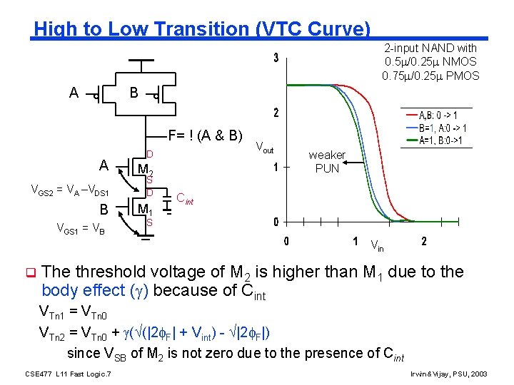
High to Low Transition (VTC Curve) 2 -input NAND with 0. 5 /0. 25 NMOS 0. 75 /0. 25 PMOS A B F= ! (A & B) A D M 2 VGS 2 = VA –VDS 1 S D B M 1 VGS 1 = VB Vout weaker PUN Cint S Vin q The threshold voltage of M 2 is higher than M 1 due to the body effect ( ) because of Cint VTn 1 = VTn 0 VTn 2 = VTn 0 + ( (|2 F| + Vint) - |2 F|) since VSB of M 2 is not zero due to the presence of Cint CSE 477 L 11 Fast Logic. 7 Irwin&Vijay, PSU, 2003

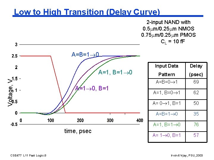
Low to High Transition (Delay Curve) 2 -input NAND with 0. 5 m/0. 25 m NMOS 0. 75 m/0. 25 m PMOS CL = 10 f. F A=B=1 0 Voltage, V A=1, B=1 0 A=1 0, B=1 time, psec CSE 477 L 11 Fast Logic. 8 Input Data Delay Pattern (psec) A=B=0 1 69 A=1, B=0 1 62 A= 0 1, B=1 50 A=B=1 0 35 A=1, B=1 0 76 A= 1 0, B=1 57 Irwin&Vijay, PSU, 2003

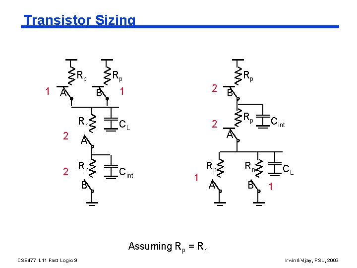
Transistor Sizing Rp 1 A Rp B Rn 2 A 2 Rn B Rp 2 B 1 CL Cint 2 1 Rp Cint A Rn Rn A B CL 1 Assuming Rp = Rn CSE 477 L 11 Fast Logic. 9 Irwin&Vijay, PSU, 2003

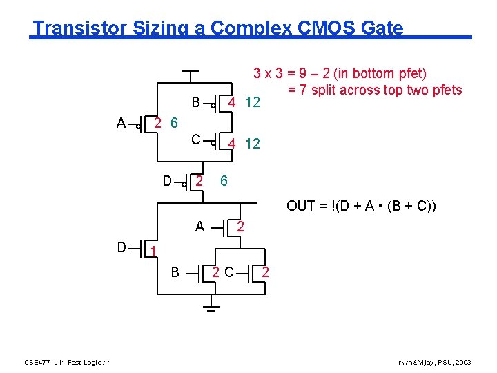
Transistor Sizing a Complex CMOS Gate A B 3 x 3 = 9 – 2 (in bottom pfet) = 7 split across top two pfets 4 12 C 4 12 2 6 D 2 6 OUT = !(D + A • (B + C)) A D 1 B CSE 477 L 11 Fast Logic. 11 2 2 C 2 Irwin&Vijay, PSU, 2003

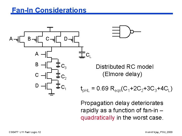
Fan-In Considerations A B C D A CL B C 3 C C 2 D C 1 Distributed RC model (Elmore delay) tp. HL = 0. 69 Reqn(C 1+2 C 2+3 C 3+4 CL) Propagation delay deteriorates rapidly as a function of fan-in – quadratically in the worst case. CSE 477 L 11 Fast Logic. 12 Irwin&Vijay, PSU, 2003

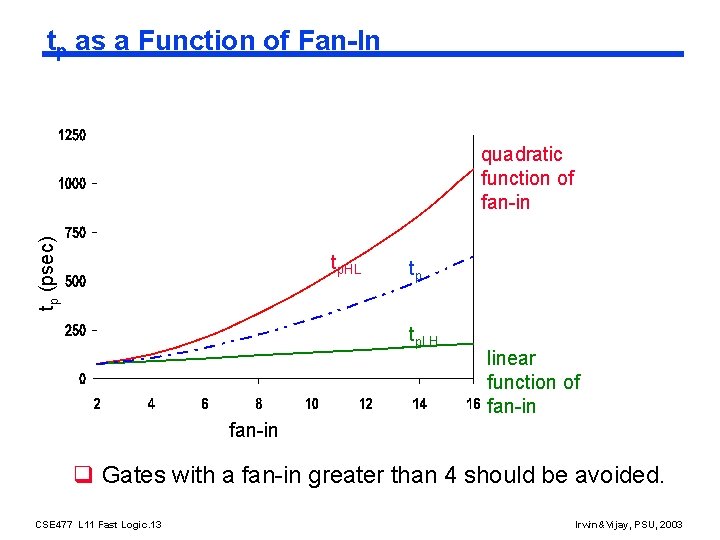
tp as a Function of Fan-In tp (psec) quadratic function of fan-in tp. HL tp tp. LH linear function of fan-in q Gates with a fan-in greater than 4 should be avoided. CSE 477 L 11 Fast Logic. 13 Irwin&Vijay, PSU, 2003

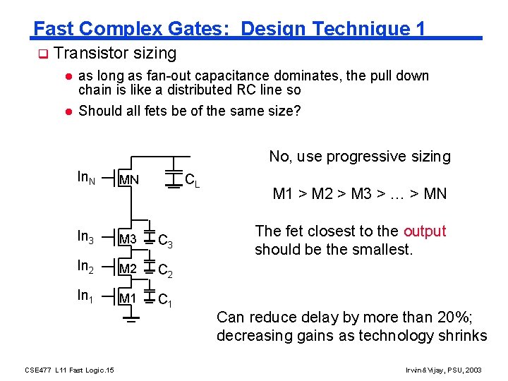
Fast Complex Gates: Design Technique 1 q Transistor sizing l l as long as fan-out capacitance dominates, the pull down chain is like a distributed RC line so Should all fets be of the same size? No, use progressive sizing In. N MN In 3 M 3 C 3 In 2 M 2 C 2 In 1 M 1 CSE 477 L 11 Fast Logic. 15 CL M 1 > M 2 > M 3 > … > MN The fet closest to the output should be the smallest. Can reduce delay by more than 20%; decreasing gains as technology shrinks Irwin&Vijay, PSU, 2003

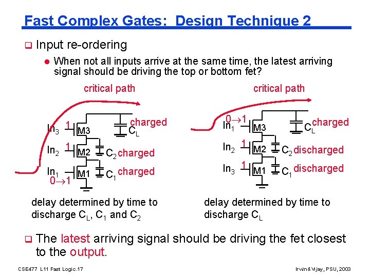
Fast Complex Gates: Design Technique 2 q Input re-ordering l When not all inputs arrive at the same time, the latest arriving signal should be driving the top or bottom fet? critical path In 3 1 M 3 charged CL In 2 1 M 2 C 2 charged In 1 M 1 0 1 C 1 charged delay determined by time to discharge CL, C 1 and C 2 q critical path 0 1 In 1 M 3 CLcharged In 2 1 M 2 C 2 discharged In 3 1 M 1 C 1 discharged delay determined by time to discharge CL The latest arriving signal should be driving the fet closest to the output. CSE 477 L 11 Fast Logic. 17 Irwin&Vijay, PSU, 2003

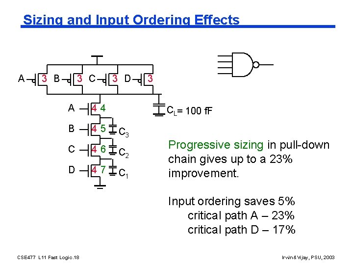
Sizing and Input Ordering Effects A 3 B 3 C 3 D A 44 B 45 C 46 C 2 D 47 C 1 3 CL= 100 f. F C 3 Progressive sizing in pull-down chain gives up to a 23% improvement. Input ordering saves 5% critical path A – 23% critical path D – 17% CSE 477 L 11 Fast Logic. 18 Irwin&Vijay, PSU, 2003

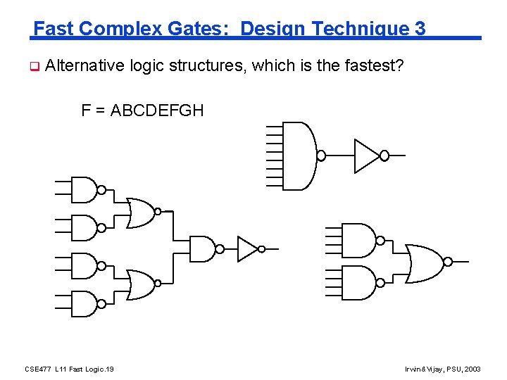
Fast Complex Gates: Design Technique 3 q Alternative logic structures, which is the fastest? F = ABCDEFGH CSE 477 L 11 Fast Logic. 19 Irwin&Vijay, PSU, 2003

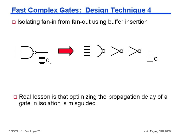
Fast Complex Gates: Design Technique 4 q Isolating fan-in from fan-out using buffer insertion CL q CL Real lesson is that optimizing the propagation delay of a gate in isolation is misguided. CSE 477 L 11 Fast Logic. 20 Irwin&Vijay, PSU, 2003

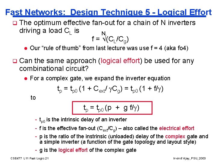
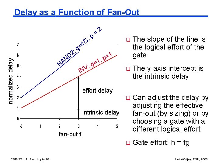
Fast Networks: Design Technique 5 - Logical Effort q The optimum effective fan-out for a chain of N inverters driving a load CL is N f = (CL/Cg) l q Our “rule of thumb” from last lecture was use f = 4 (aka fo 4) Can the same approach (logical effort) be used for any combinational circuit? l For a complex gate, we expand the inverter equation tp = tp 0 (1 + Cext/ Cg) = tp 0 (1 + f/ ) to tp = tp 0 (p + g f/ ) - tp 0 is the intrinsic delay of an inverter - f is the effective fan-out (Cext/Cg) – also called the electrical effort - p is the ratio of the instrinsic (unloaded) delay of the complex gate and a simple inverter (a function of the gate topology and layout style) - g is the logical effort of the complex gate CSE 477 L 11 Fast Logic. 21 Irwin&Vijay, PSU, 2003

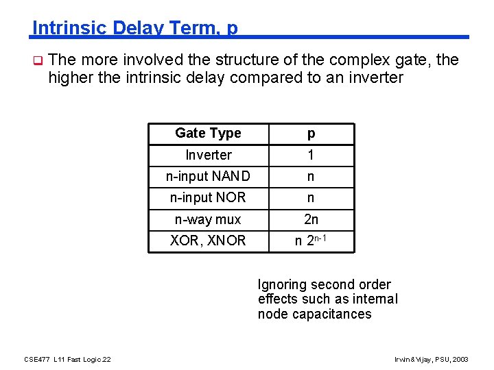
Intrinsic Delay Term, p q The more involved the structure of the complex gate, the higher the intrinsic delay compared to an inverter Gate Type p Inverter 1 n-input NAND n n-input NOR n n-way mux 2 n XOR, XNOR n 2 n-1 Ignoring second order effects such as internal node capacitances CSE 477 L 11 Fast Logic. 22 Irwin&Vijay, PSU, 2003

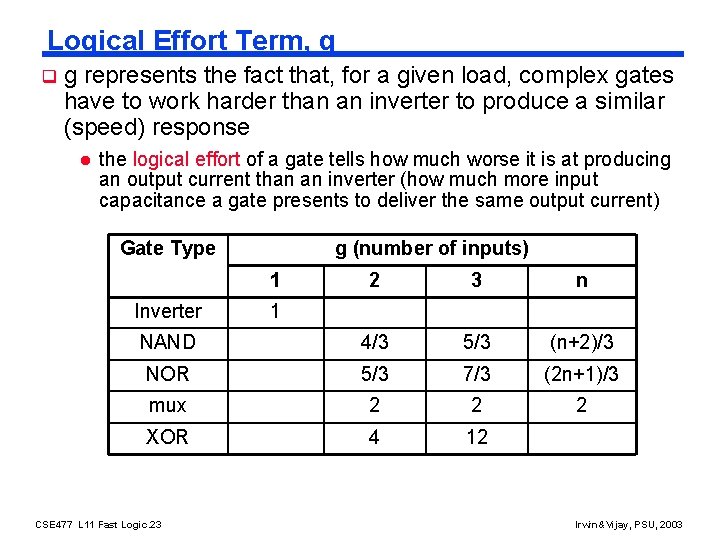
Logical Effort Term, g q g represents the fact that, for a given load, complex gates have to work harder than an inverter to produce a similar (speed) response l the logical effort of a gate tells how much worse it is at producing an output current than an inverter (how much more input capacitance a gate presents to deliver the same output current) Gate Type g (number of inputs) 1 2 3 n NAND 4/3 5/3 (n+2)/3 NOR 5/3 7/3 (2 n+1)/3 mux 2 2 2 XOR 4 12 Inverter CSE 477 L 11 Fast Logic. 23 1 Irwin&Vijay, PSU, 2003

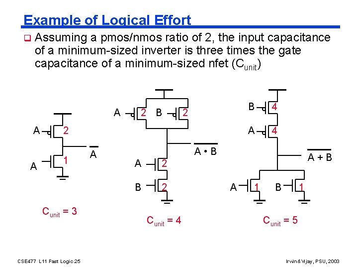
Example of Logical Effort q Assuming a pmos/nmos ratio of 2, the input capacitance of a minimum-sized inverter is three times the gate capacitance of a minimum-sized nfet (Cunit) A A A 2 B 2 2 1 Cunit = 3 CSE 477 L 11 Fast Logic. 25 A B 4 A • B A 2 B 2 Cunit = 4 A+B A 1 B 1 Cunit = 5 Irwin&Vijay, PSU, 2003

Delay as a Function of Fan-Out = normalized delay g : 2 p , 3 2 4/ D N A N = The slope of the line is the logical effort of the gate q The y-axis intercept is the intrinsic delay q Can adjust the delay by adjusting the effective fan-out (by sizing) or by choosing a gate with a different logical effort q Gate effort: h = fg =1 p 1, = g V: q IN effort delay intrinsic delay fan-out f CSE 477 L 11 Fast Logic. 26 Irwin&Vijay, PSU, 2003

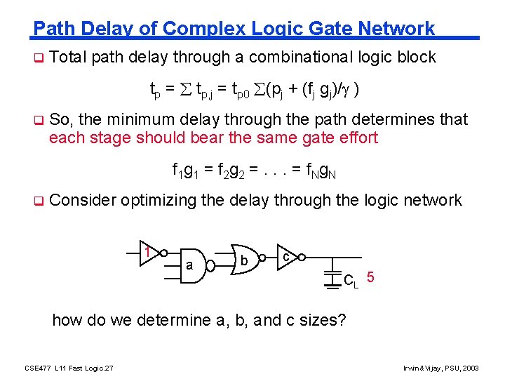
Path Delay of Complex Logic Gate Network q Total path delay through a combinational logic block tp = tp, j = tp 0 (pj + (fj gj)/ ) q So, the minimum delay through the path determines that each stage should bear the same gate effort f 1 g 1 = f 2 g 2 =. . . = f Ng N q Consider optimizing the delay through the logic network 1 a b c CL 5 how do we determine a, b, and c sizes? CSE 477 L 11 Fast Logic. 27 Irwin&Vijay, PSU, 2003

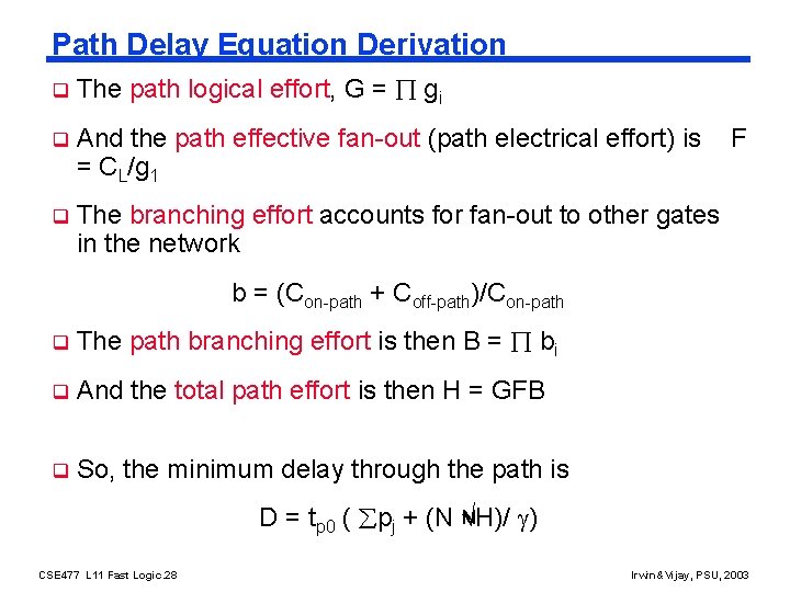
Path Delay Equation Derivation q The path logical effort, G = gi q And the path effective fan-out (path electrical effort) is = CL/g 1 q The branching effort accounts for fan-out to other gates in the network F b = (Con-path + Coff-path)/Con-path q The path branching effort is then B = bi q And the total path effort is then H = GFB q So, the minimum delay through the path is N D = tp 0 ( pj + (N H)/ ) CSE 477 L 11 Fast Logic. 28 Irwin&Vijay, PSU, 2003

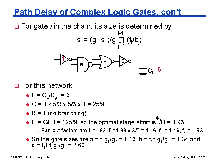
Path Delay of Complex Logic Gates, con’t q For gate i in the chain, its size is determined by i-1 si = (g 1 s 1)/gi (fj/bj) j=1 1 q a b c CL 5 For this network l F = CL/Cg 1 = 5 G = 1 x 5/3 x 1 = 25/9 B = 1 (no branching) l H = GFB = 125/9, so the optimal stage effort is H = 1. 93 l l 4 - Fan-out factors are f 1=1. 93, f 2=1. 93 x 3/5 = 1. 16, f 3 = 1. 16, f 4 = 1. 93 l So the gate sizes are a = f 1 g 1/g 2 = 1. 16, b = f 1 f 2 g 1/g 3 = 1. 34 and c = f 1 f 2 f 3 g 1/g 4 = 2. 60 CSE 477 L 11 Fast Logic. 29 Irwin&Vijay, PSU, 2003

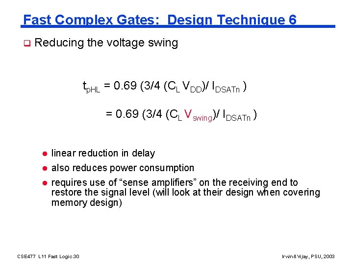
Fast Complex Gates: Design Technique 6 q Reducing the voltage swing tp. HL = 0. 69 (3/4 (CL VDD)/ IDSATn ) = 0. 69 (3/4 (CL Vswing)/ IDSATn ) l linear reduction in delay also reduces power consumption requires use of “sense amplifiers” on the receiving end to restore the signal level (will look at their design when covering memory design) CSE 477 L 11 Fast Logic. 30 Irwin&Vijay, PSU, 2003

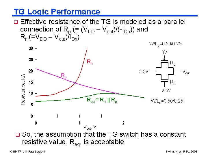
TG Logic Performance q Effective resistance of the TG is modeled as a parallel connection of Rp (= (VDD – Vout)/(-IDp)) and Rn (=VDD – Vout)/IDn) W/Lp=0. 50/0. 25 0 V Resistance, k Rn Rp 2. 5 V Rp Vout Rn 2. 5 V Req = Rn || Rp W/Ln=0. 50/0. 25 Vout, V q So, the assumption that the TG switch has a constant resistive value, Req, is acceptable CSE 477 L 11 Fast Logic. 31 Irwin&Vijay, PSU, 2003

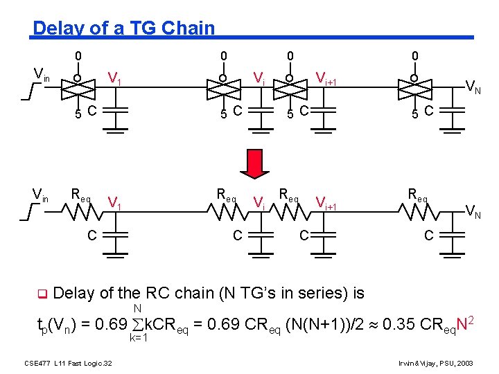
Delay of a TG Chain 0 0 Vin V 1 Req 5 C Req V 1 C q 0 Vi 5 C Vin 0 C Vi+1 5 C Vi Req VN 5 C Vi+1 C Req VN C Delay of the RC chain (N TG’s in series) is N tp(Vn) = 0. 69 k. CReq = 0. 69 CReq (N(N+1))/2 0. 35 CReq. N 2 k=1 CSE 477 L 11 Fast Logic. 32 Irwin&Vijay, PSU, 2003

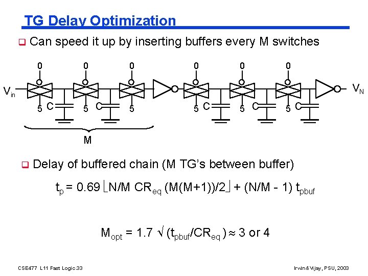
TG Delay Optimization q Can speed it up by inserting buffers every M switches 0 0 0 VN Vin 5 C 5 C 5 C M q Delay of buffered chain (M TG’s between buffer) tp = 0. 69 N/M CReq (M(M+1))/2 + (N/M - 1) tpbuf Mopt = 1. 7 (tpbuf/CReq ) 3 or 4 CSE 477 L 11 Fast Logic. 33 Irwin&Vijay, PSU, 2003

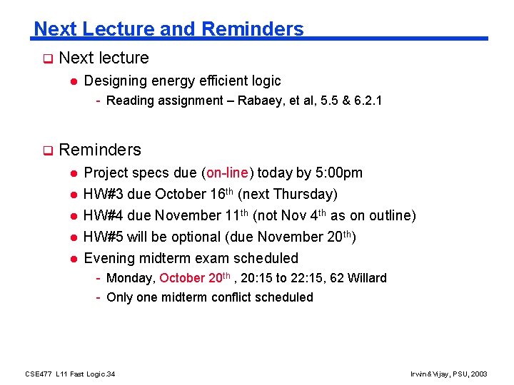
Next Lecture and Reminders q Next lecture l Designing energy efficient logic - Reading assignment – Rabaey, et al, 5. 5 & 6. 2. 1 q Reminders l Project specs due (on-line) today by 5: 00 pm l HW#3 due October 16 th (next Thursday) l HW#4 due November 11 th (not Nov 4 th as on outline) l HW#5 will be optional (due November 20 th) Evening midterm exam scheduled l - Monday, October 20 th , 20: 15 to 22: 15, 62 Willard - Only one midterm conflict scheduled CSE 477 L 11 Fast Logic. 34 Irwin&Vijay, PSU, 2003