CSE 477 VLSI Digital Circuits Fall 2003 Lecture
![4 x 4 CAM Design 0 1 Hit WL[0] WL[1] WL[2] WL[3] 1 1 4 x 4 CAM Design 0 1 Hit WL[0] WL[1] WL[2] WL[3] 1 1](https://slidetodoc.com/presentation_image_h2/f00d3eb12296bd3ec709324875e17833/image-20.jpg)
- Slides: 21

CSE 477 VLSI Digital Circuits Fall 2003 Lecture 24: Memory Cell Designs Mary Jane Irwin ( www. cse. psu. edu/~mji ) www. cse. psu. edu/~cg 477 [Adapted from Rabaey’s Digital Integrated Circuits, Second Edition, © 2003 Rabaey, A. Chandrakasan, B. Nikolic] CSE 477 L 24 RAM Cores. 1 J. Irwin&Vijay, PSU, 2003

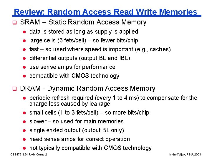
Review: Random Access Read Write Memories q SRAM – Static Random Access Memory l data is stored as long as supply is applied large cells (6 fets/cell) – so fewer bits/chip fast – so used where speed is important (e. g. , caches) l differential outputs (output BL and !BL) l use sense amps for performance l compatible with CMOS technology l l q DRAM - Dynamic Random Access Memory l l l periodic refresh required (every 1 to 4 ms) to compensate for the charge loss caused by leakage small cells (1 to 3 fets/cell) – so more bits/chip slower – so used for main memories single ended output (output BL only) need sense amps for correct operation not typically compatible with CMOS technology CSE 477 L 24 RAM Cores. 2 Irwin&Vijay, PSU, 2003

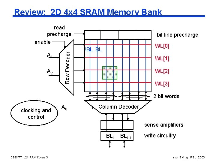
Review: 2 D 4 x 4 SRAM Memory Bank A 1 A 2 Row Decoder read precharge enable bit line precharge WL[0] !BL BL WL[1] WL[2] WL[3] 2 bit words clocking and control A 0 Column Decoder sense amplifiers BLi CSE 477 L 24 RAM Cores. 3 BLi+1 write circuitry Irwin&Vijay, PSU, 2003

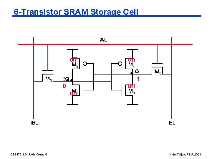
6 -Transistor SRAM Storage Cell WL off M 2 on M 4 Q M 5 !BL CSE 477 L 24 RAM Cores. 5 1 !Q 0 M 6 M 1 on off M 3 BL Irwin&Vijay, PSU, 2003

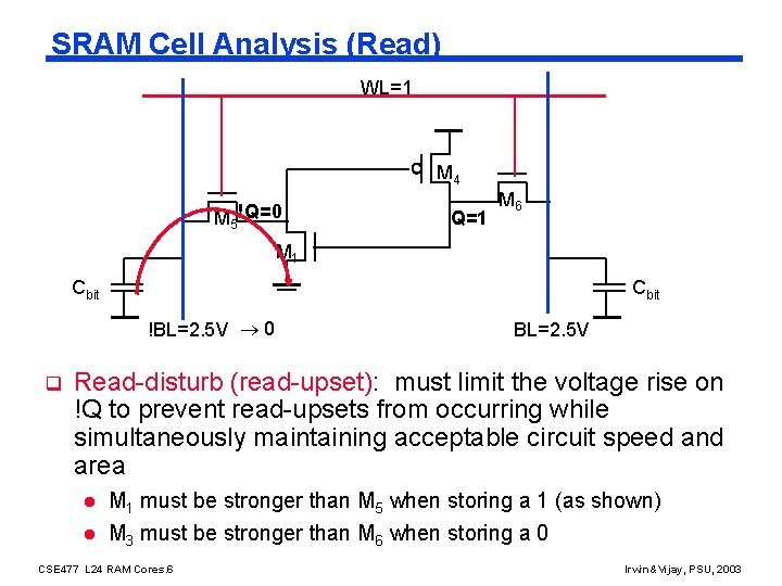
SRAM Cell Analysis (Read) WL=1 M 4 M 5 !Q=0 Q=1 M 6 M 1 Cbit !BL=2. 5 V 0 q BL=2. 5 V Read-disturb (read-upset): must limit the voltage rise on !Q to prevent read-upsets from occurring while simultaneously maintaining acceptable circuit speed and area l M 1 must be stronger than M 5 when storing a 1 (as shown) l M 3 must be stronger than M 6 when storing a 0 CSE 477 L 24 RAM Cores. 6 Irwin&Vijay, PSU, 2003

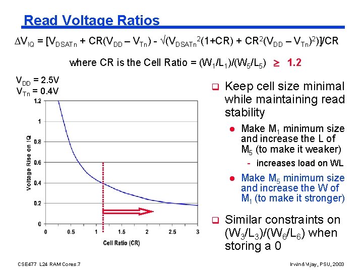
Read Voltage Ratios V!Q = [VDSATn + CR(VDD – VTn) - (VDSATn 2(1+CR) + CR 2(VDD – VTn)2)]/CR where CR is the Cell Ratio = (W 1/L 1)/(W 5/L 5) 1. 2 VDD = 2. 5 V VTn = 0. 4 V q Keep cell size minimal while maintaining read stability l Make M 1 minimum size and increase the L of M 5 (to make it weaker) - increases load on WL l q CSE 477 L 24 RAM Cores. 7 Make M 5 minimum size and increase the W of M 1 (to make it stronger) Similar constraints on (W 3/L 3)/(W 6/L 6) when storing a 0 Irwin&Vijay, PSU, 2003

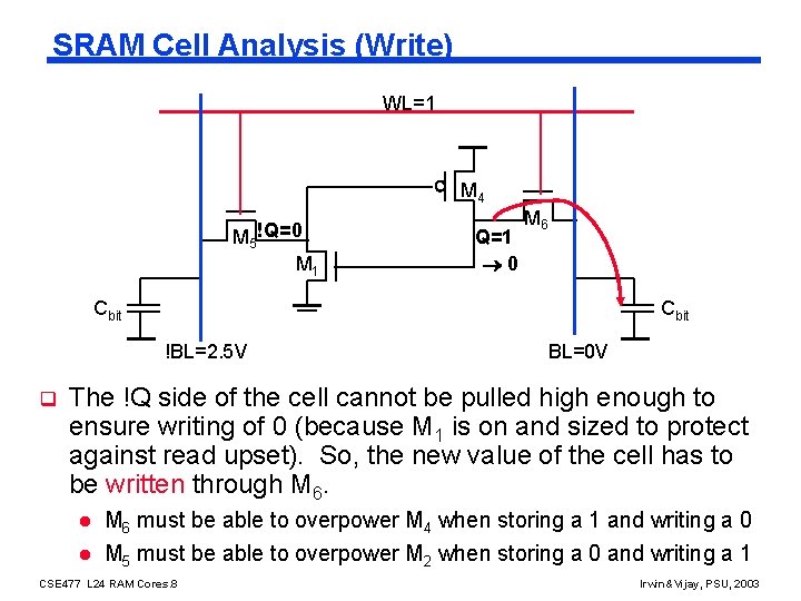
SRAM Cell Analysis (Write) WL=1 M 4 M 5 !Q=0 M 1 Q=1 0 M 6 Cbit !BL=2. 5 V q BL=0 V The !Q side of the cell cannot be pulled high enough to ensure writing of 0 (because M 1 is on and sized to protect against read upset). So, the new value of the cell has to be written through M 6. l M 6 must be able to overpower M 4 when storing a 1 and writing a 0 l M 5 must be able to overpower M 2 when storing a 0 and writing a 1 CSE 477 L 24 RAM Cores. 8 Irwin&Vijay, PSU, 2003

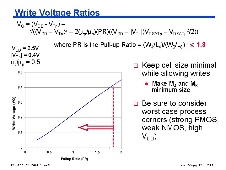
Write Voltage Ratios VQ = (VDD - VTn) – ((VDD – VTn)2 – 2( p/ n)(PR)((VDD – |VTp|)VDSATp – VDSATp 2/2)) VDD = 2. 5 V |VTp| = 0. 4 V p/ n = 0. 5 where PR is the Pull-up Ratio = (W 4/L 4)/(W 6/L 6) 1. 8 q Keep cell size minimal while allowing writes l q CSE 477 L 24 RAM Cores. 9 Make M 4 and M 6 minimum size Be sure to consider worst case process corners (strong PMOS, weak NMOS, high VDD) Irwin&Vijay, PSU, 2003

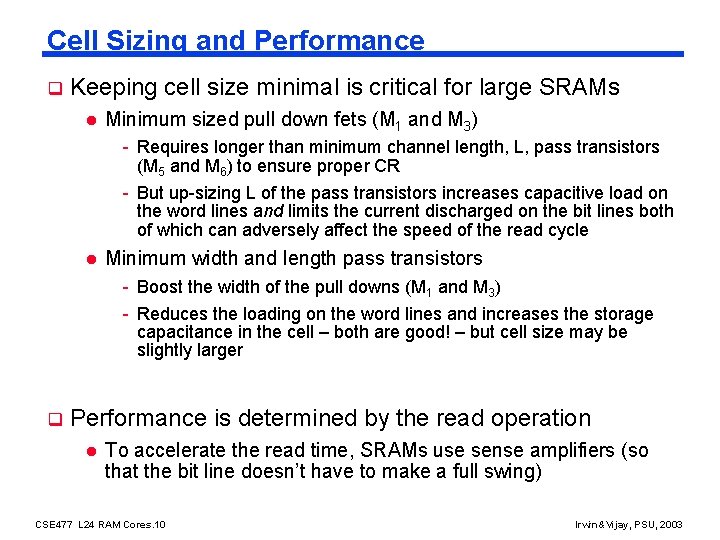
Cell Sizing and Performance q Keeping cell size minimal is critical for large SRAMs l Minimum sized pull down fets (M 1 and M 3) - Requires longer than minimum channel length, L, pass transistors (M 5 and M 6) to ensure proper CR - But up-sizing L of the pass transistors increases capacitive load on the word lines and limits the current discharged on the bit lines both of which can adversely affect the speed of the read cycle l Minimum width and length pass transistors - Boost the width of the pull downs (M 1 and M 3) - Reduces the loading on the word lines and increases the storage capacitance in the cell – both are good! – but cell size may be slightly larger q Performance is determined by the read operation l To accelerate the read time, SRAMs use sense amplifiers (so that the bit line doesn’t have to make a full swing) CSE 477 L 24 RAM Cores. 10 Irwin&Vijay, PSU, 2003

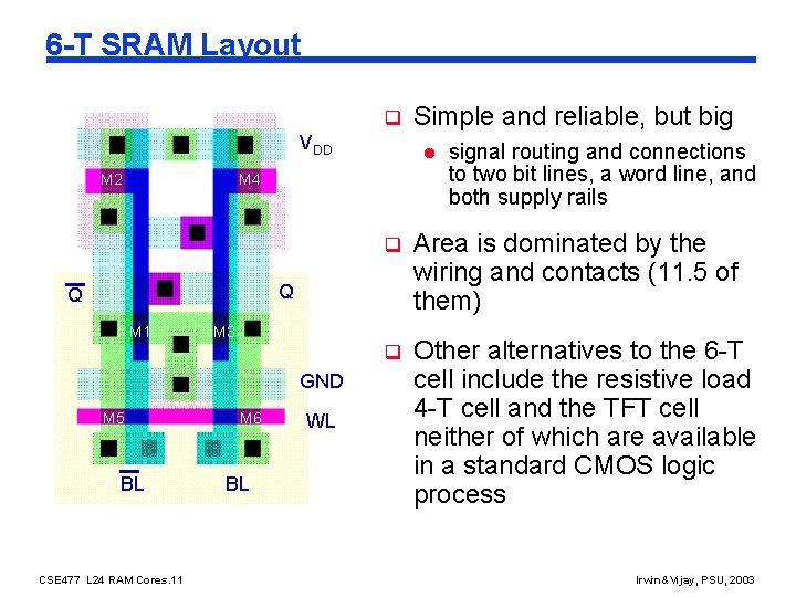
6 -T SRAM Layout q VDD M 2 l M 4 M 1 M 3 GND M 5 BL CSE 477 L 24 RAM Cores. 11 M 6 BL WL signal routing and connections to two bit lines, a word line, and both supply rails q Area is dominated by the wiring and contacts (11. 5 of them) q Other alternatives to the 6 -T cell include the resistive load 4 -T cell and the TFT cell neither of which are available in a standard CMOS logic process Q Q Simple and reliable, but big Irwin&Vijay, PSU, 2003

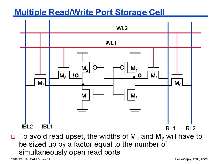
Multiple Read/Write Port Storage Cell WL 2 WL 1 M 2 M 5 M 4 !Q Q M 7 M 8 M 1 !BL 2 q !BL 1 M 6 M 3 BL 1 BL 2 To avoid read upset, the widths of M 1 and M 3 will have to be sized up by a factor equal to the number of simultaneously open read ports CSE 477 L 24 RAM Cores. 12 Irwin&Vijay, PSU, 2003

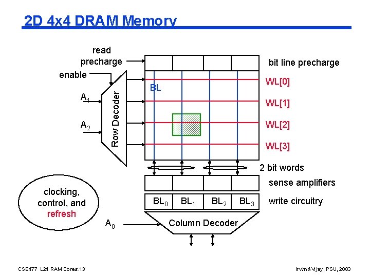
2 D 4 x 4 DRAM Memory A 1 A 2 Row Decoder read precharge enable bit line precharge WL[0] BL WL[1] WL[2] WL[3] 2 bit words clocking, control, and refresh CSE 477 L 24 RAM Cores. 13 sense amplifiers BL 0 A 0 BL 1 BL 2 BL 3 write circuitry Column Decoder Irwin&Vijay, PSU, 2003

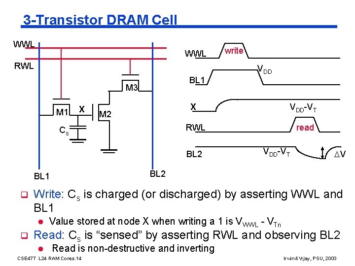
3 -Transistor DRAM Cell WWL RWL VDD BL 1 M 3 M 1 X M 2 Cs X VDD-VT RWL read BL 2 V Write: Cs is charged (or discharged) by asserting WWL and BL 1 l q VDD-VT BL 2 BL 1 q write Value stored at node X when writing a 1 is VWWL - VTn Read: Cs is “sensed” by asserting RWL and observing BL 2 l Read is non-destructive and inverting CSE 477 L 24 RAM Cores. 14 Irwin&Vijay, PSU, 2003

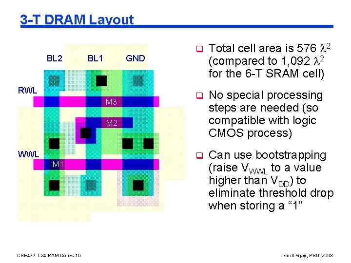
3 -T DRAM Layout BL 2 BL 1 GND RWL M 3 q Total cell area is 576 2 (compared to 1, 092 2 for the 6 -T SRAM cell) q No special processing steps are needed (so compatible with logic CMOS process) q Can use bootstrapping (raise VWWL to a value higher than VDD) to eliminate threshold drop when storing a “ 1” M 2 WWL M 1 CSE 477 L 24 RAM Cores. 15 Irwin&Vijay, PSU, 2003

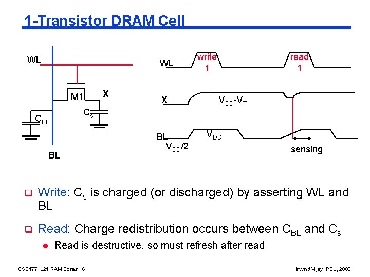
1 -Transistor DRAM Cell WL WL M 1 X X write 1 read 1 VDD-VT Cs CBL BL BL VDD/2 VDD sensing q Write: Cs is charged (or discharged) by asserting WL and BL q Read: Charge redistribution occurs between CBL and Cs l Read is destructive, so must refresh after read CSE 477 L 24 RAM Cores. 16 Irwin&Vijay, PSU, 2003

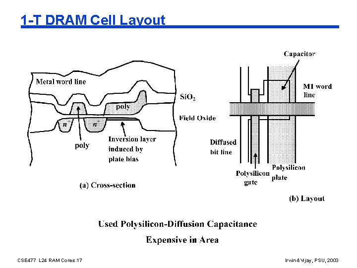
1 -T DRAM Cell Layout CSE 477 L 24 RAM Cores. 17 Irwin&Vijay, PSU, 2003

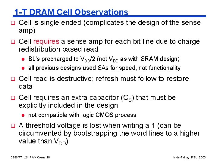
1 -T DRAM Cell Observations q Cell is single ended (complicates the design of the sense amp) q Cell requires a sense amp for each bit line due to charge redistribution based read l BL’s precharged to VDD/2 (not VDD as with SRAM design) l all previous designs used SAs for speed, not functionality q Cell read is destructive; refresh must follow to restore data q Cell requires an extra capacitor (CS) that must be explicitly included in the design l q not compatible with logic CMOS process A threshold voltage is lost when writing a 1 (can be circumvented by bootstrapping the word lines to a higher value than VDD) CSE 477 L 24 RAM Cores. 18 Irwin&Vijay, PSU, 2003

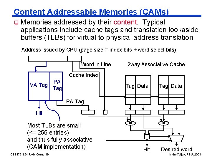
Content Addressable Memories (CAMs) q Memories addressed by their content. Typical applications include cache tags and translation lookaside buffers (TLBs) for virtual to physical address translation Address issued by CPU (page size = index bits + word select bits) Word in Line 2 way Associative Cache Index VA Tag PA Tag Data PA Tag Hit Most TLBs are small (<= 256 entries) and thus fully associative (CAM implementation) CSE 477 L 24 RAM Cores. 19 = = Hit Desired word Irwin&Vijay, PSU, 2003

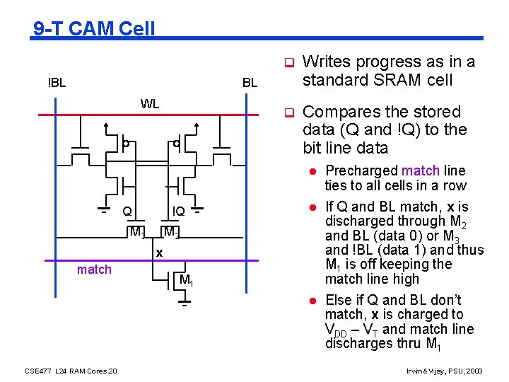
9 -T CAM Cell !BL q Writes progress as in a standard SRAM cell q Compares the stored data (Q and !Q) to the bit line data BL WL Q !Q M 3 l Precharged match line ties to all cells in a row l If Q and BL match, x is discharged through M 2 and BL (data 0) or M 3 and !BL (data 1) and thus M 1 is off keeping the match line high Else if Q and BL don’t match, x is charged to VDD – VT and match line discharges thru M 1 M 2 x match M 1 l CSE 477 L 24 RAM Cores. 20 Irwin&Vijay, PSU, 2003
![4 x 4 CAM Design 0 1 Hit WL0 WL1 WL2 WL3 1 1 4 x 4 CAM Design 0 1 Hit WL[0] WL[1] WL[2] WL[3] 1 1](https://slidetodoc.com/presentation_image_h2/f00d3eb12296bd3ec709324875e17833/image-20.jpg)
4 x 4 CAM Design 0 1 Hit WL[0] WL[1] WL[2] WL[3] 1 1 0 0 1 1 1 0 0 0 match[0] 1 0 match[1] 1 1 match[2] 1 0 to WL[0] of data array match[3] 1 0 Read/Write Circuitry match/write data 1 011 precharge/match 0 1 CSE 477 L 24 RAM Cores. 22 Irwin&Vijay, PSU, 2003

Next Lecture and Reminders q Next lecture l Peripheral memory circuits - Reading assignment – Rabaey, et al, 12. 3 -12. 4 q Reminders l HW#5 (optional) due December 2 nd l Project final reports due December 4 th l Final grading negotiations/correction (except for the final exam) must be concluded by December 10 th Final exam scheduled l - Tuesday, December 16 th from 10: 10 to noon in 118 and 113 Thomas CSE 477 L 24 RAM Cores. 23 Irwin&Vijay, PSU, 2003