CSE 477 VLSI Digital Circuits Fall 2003 Lecture
- Slides: 25

CSE 477 VLSI Digital Circuits Fall 2003 Lecture 23: Semiconductor Memories Mary Jane Irwin ( www. cse. psu. edu/~mji ) www. cse. psu. edu/~cg 477 [Adapted from Rabaey’s Digital Integrated Circuits, Second Edition, © 2003 Rabaey, A. Chandrakasan, B. Nikolic] CSE 477 L 23 Memories. 1 J. Irwin&Vijay, PSU, 2003

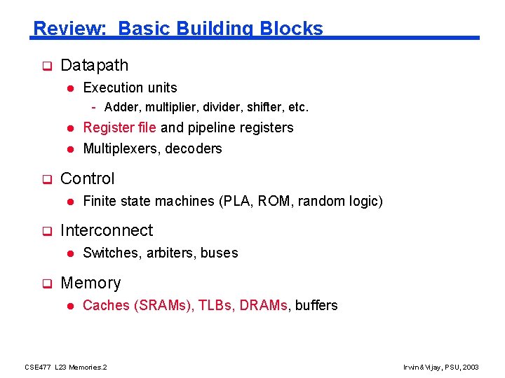
Review: Basic Building Blocks q Datapath l Execution units - Adder, multiplier, divider, shifter, etc. q l Register file and pipeline registers l Multiplexers, decoders Control l q Interconnect l q Finite state machines (PLA, ROM, random logic) Switches, arbiters, buses Memory l Caches (SRAMs), TLBs, DRAMs, buffers CSE 477 L 23 Memories. 2 Irwin&Vijay, PSU, 2003

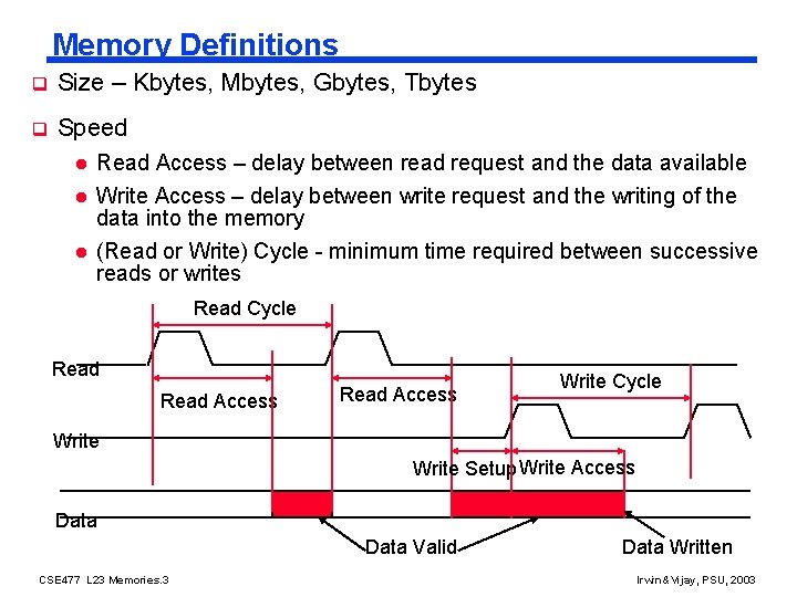
Memory Definitions q Size – Kbytes, Mbytes, Gbytes, Tbytes q Speed l l l Read Access – delay between read request and the data available Write Access – delay between write request and the writing of the data into the memory (Read or Write) Cycle - minimum time required between successive reads or writes Read Cycle Read Access Write Cycle Write Setup Write Access Data Valid CSE 477 L 23 Memories. 3 Data Written Irwin&Vijay, PSU, 2003

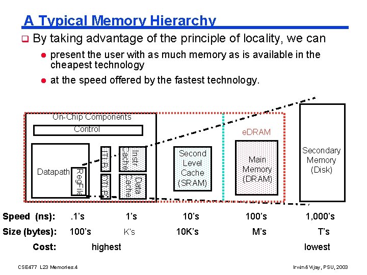
A Typical Memory Hierarchy q By taking advantage of the principle of locality, we can l l present the user with as much memory as is available in the cheapest technology at the speed offered by the fastest technology. On-Chip Components Control e. DRAM Instr Data Cache . 1’s 10’s 100’s Size (bytes): 100’s K’s 10 K’s M’s Cost: CSE 477 L 23 Memories. 4 ITLB DTLB Speed (ns): Datapath Reg. File Second Level Cache (SRAM) highest Main Memory (DRAM) Secondary Memory (Disk) 1, 000’s T’s lowest Irwin&Vijay, PSU, 2003

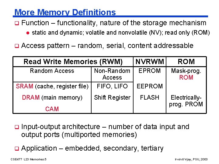
More Memory Definitions q Function – functionality, nature of the storage mechanism l q static and dynamic; volatile and nonvolatile (NV); read only (ROM) Access pattern – random, serial, content addressable Read Write Memories (RWM) Random Access Non-Random Access SRAM (cache, register file) FIFO, LIFO DRAM (main memory) Shift Register NVRWM ROM EPROM Mask-prog. ROM EEPROM FLASH CAM Electricallyprog. PROM q Input-output architecture – number of data input and output ports (multiported memories) q Application – embedded, secondary, tertiary CSE 477 L 23 Memories. 5 Irwin&Vijay, PSU, 2003

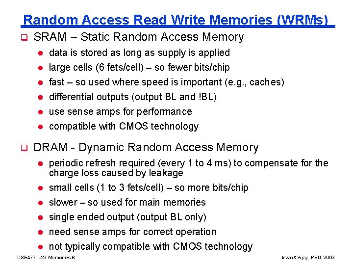
Random Access Read Write Memories (WRMs) q SRAM – Static Random Access Memory l data is stored as long as supply is applied large cells (6 fets/cell) – so fewer bits/chip fast – so used where speed is important (e. g. , caches) l differential outputs (output BL and !BL) l use sense amps for performance l compatible with CMOS technology l l q DRAM - Dynamic Random Access Memory l l l periodic refresh required (every 1 to 4 ms) to compensate for the charge loss caused by leakage small cells (1 to 3 fets/cell) – so more bits/chip slower – so used for main memories single ended output (output BL only) need sense amps for correct operation not typically compatible with CMOS technology CSE 477 L 23 Memories. 6 Irwin&Vijay, PSU, 2003

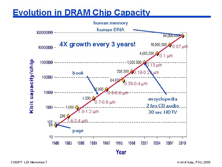
Evolution in DRAM Chip Capacity human memory human DNA 4 X growth every 3 years! 0. 07 m 0. 13 m 0. 18 -0. 25 m book 0. 35 -0. 4 m 0. 5 -0. 6 m 0. 7 -0. 8 m 1. 0 -1. 2 m encyclopedia 2 hrs CD audio 30 sec HDTV 1. 6 -2. 4 m page CSE 477 L 23 Memories. 7 Irwin&Vijay, PSU, 2003

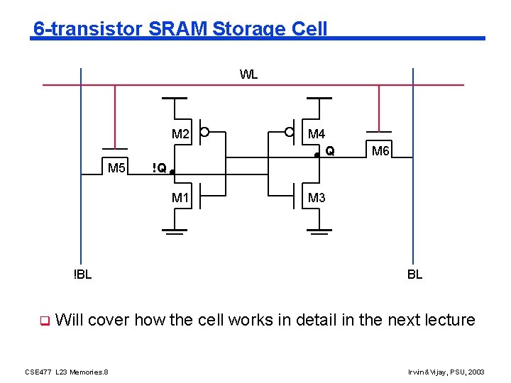
6 -transistor SRAM Storage Cell WL M 2 M 5 q M 6 !Q M 1 !BL M 4 Q M 3 BL Will cover how the cell works in detail in the next lecture CSE 477 L 23 Memories. 8 Irwin&Vijay, PSU, 2003

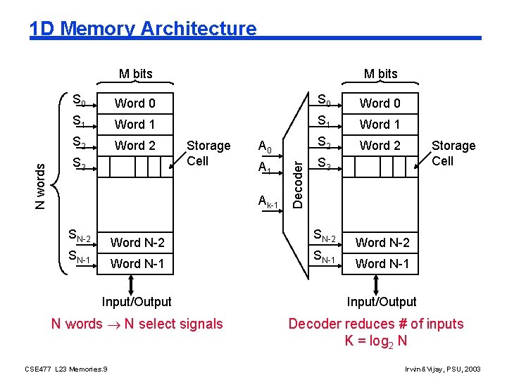
1 D Memory Architecture M bits S 0 Word 0 S 1 Word 1 S 2 Word 2 A 0 S 2 Word 2 A 1 S 3 Storage Cell Ak-1 SN-2 Word N-2 SN-1 Word N-1 Input/Output N words N select signals CSE 477 L 23 Memories. 9 Decoder N words M bits SN-2 SN-1 Storage Cell Word N-2 Word N-1 Input/Output Decoder reduces # of inputs K = log 2 N Irwin&Vijay, PSU, 2003

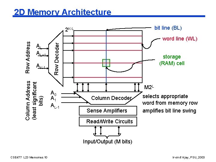
2 D Memory Architecture bit line (BL) AL AL+1 AK-1 Row Decoder word line (WL) Column Address (least significant bits) Row Address 2 K-L A 0 A 1 AL-1 storage (RAM) cell M 2 L Column Decoder Sense Amplifiers selects appropriate word from memory row amplifies bit line swing Read/Write Circuits Input/Output (M bits) CSE 477 L 23 Memories. 10 Irwin&Vijay, PSU, 2003

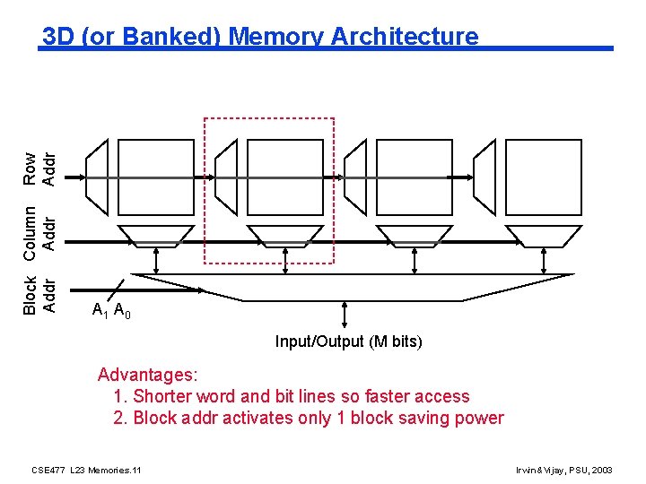
Block Column Addr Row Addr 3 D (or Banked) Memory Architecture A 1 A 0 Input/Output (M bits) Advantages: 1. Shorter word and bit lines so faster access 2. Block addr activates only 1 block saving power CSE 477 L 23 Memories. 11 Irwin&Vijay, PSU, 2003

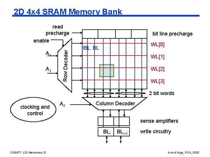
2 D 4 x 4 SRAM Memory Bank A 1 A 2 Row Decoder read precharge enable bit line precharge WL[0] !BL BL WL[1] WL[2] WL[3] 2 bit words clocking and control A 0 Column Decoder sense amplifiers BLi CSE 477 L 23 Memories. 12 BLi+1 write circuitry Irwin&Vijay, PSU, 2003

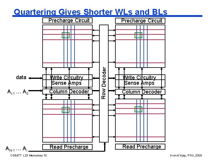
Quartering Gives Shorter WLs and BLs Precharge Circuit Write Circuitry Sense Amps Ai-1 … A 0 Column Decoder AN-1 … Ai Read Precharge CSE 477 L 23 Memories. 13 Row Decoder data Precharge Circuit Write Circuitry Sense Amps Column Decoder Read Precharge Irwin&Vijay, PSU, 2003

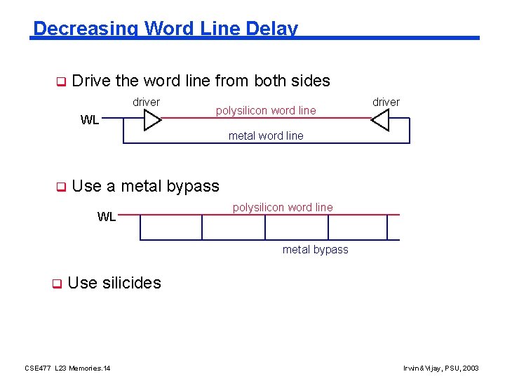
Decreasing Word Line Delay q Drive the word line from both sides driver WL polysilicon word line driver metal word line q Use a metal bypass WL polysilicon word line metal bypass q Use silicides CSE 477 L 23 Memories. 14 Irwin&Vijay, PSU, 2003

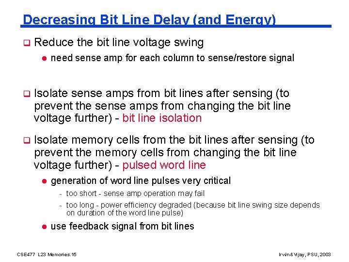
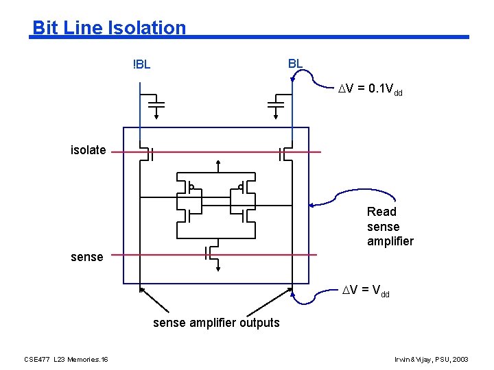
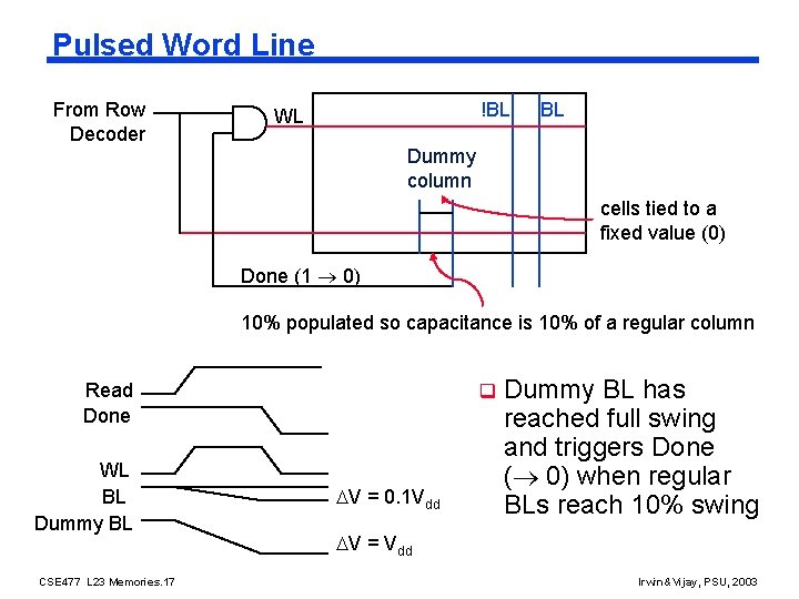
Decreasing Bit Line Delay (and Energy) q Reduce the bit line voltage swing l need sense amp for each column to sense/restore signal q Isolate sense amps from bit lines after sensing (to prevent the sense amps from changing the bit line voltage further) - bit line isolation q Isolate memory cells from the bit lines after sensing (to prevent the memory cells from changing the bit line voltage further) - pulsed word line l generation of word line pulses very critical - too short - sense amp operation may fail - too long - power efficiency degraded (because bit line swing size depends on duration of the word line pulse) l use feedback signal from bit lines CSE 477 L 23 Memories. 15 Irwin&Vijay, PSU, 2003

Bit Line Isolation BL !BL V = 0. 1 Vdd isolate Read sense amplifier sense V = Vdd sense amplifier outputs CSE 477 L 23 Memories. 16 Irwin&Vijay, PSU, 2003

Pulsed Word Line From Row Decoder !BL WL BL Dummy column cells tied to a fixed value (0) Done (1 0) 10% populated so capacitance is 10% of a regular column Read Done WL BL Dummy BL CSE 477 L 23 Memories. 17 q V = 0. 1 Vdd Dummy BL has reached full swing and triggers Done ( 0) when regular BLs reach 10% swing V = Vdd Irwin&Vijay, PSU, 2003

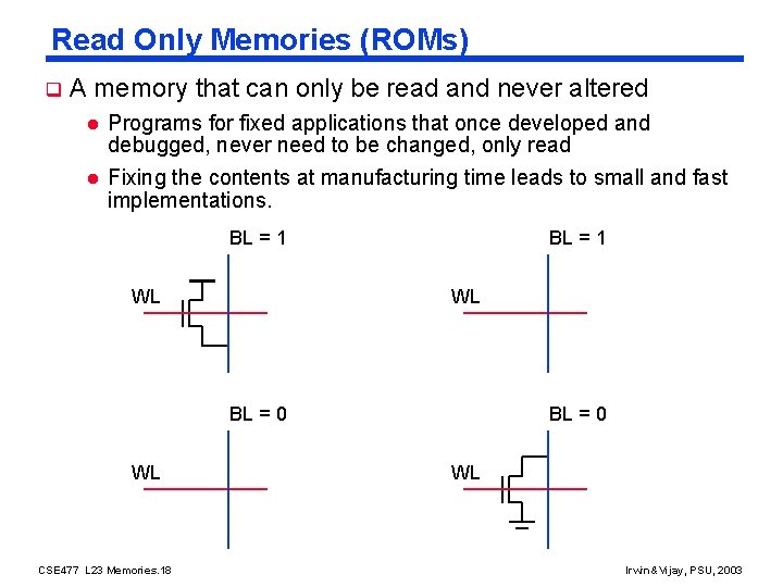
Read Only Memories (ROMs) q A memory that can only be read and never altered l l Programs for fixed applications that once developed and debugged, never need to be changed, only read Fixing the contents at manufacturing time leads to small and fast implementations. BL = 1 WL BL = 0 WL CSE 477 L 23 Memories. 18 BL = 0 WL Irwin&Vijay, PSU, 2003

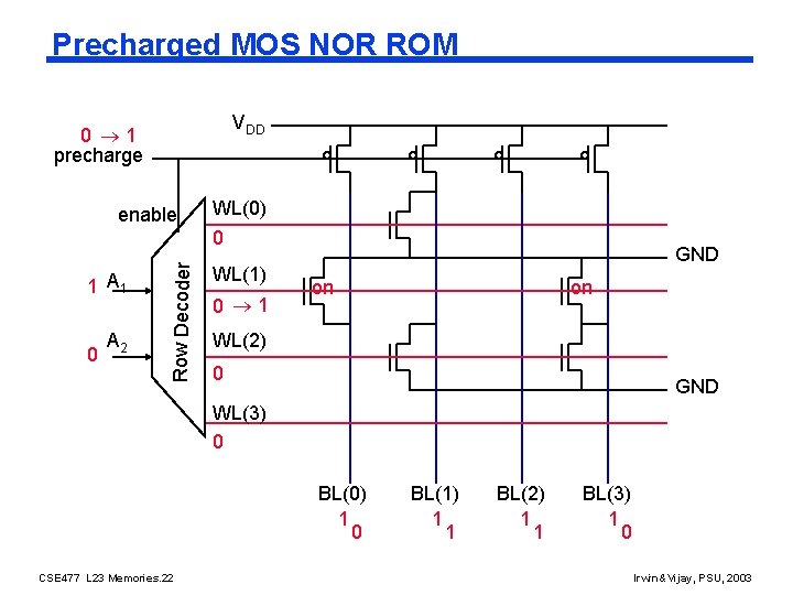
Precharged MOS NOR ROM VDD 0 1 precharge 1 A 1 0 A 2 Row Decoder enable WL(0) 0 WL(1) 0 1 GND on on WL(2) 0 GND WL(3) 0 BL(0) 1 0 CSE 477 L 23 Memories. 22 BL(1) 1 1 BL(2) 1 1 BL(3) 1 0 Irwin&Vijay, PSU, 2003

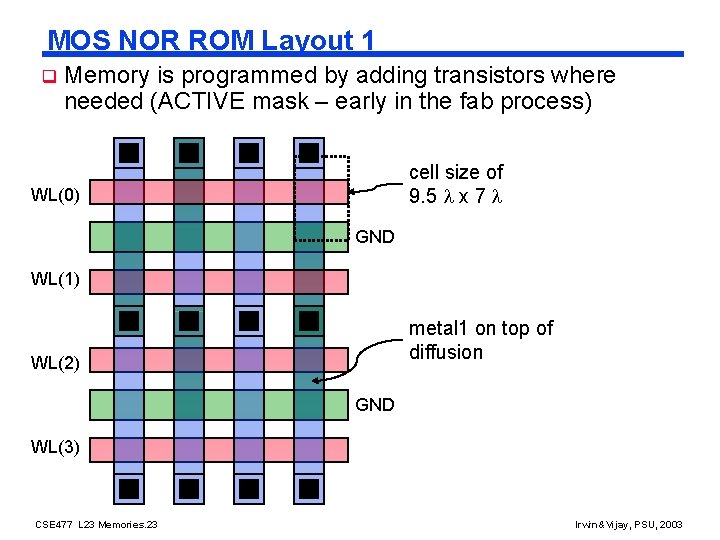
MOS NOR ROM Layout 1 q Memory is programmed by adding transistors where needed (ACTIVE mask – early in the fab process) cell size of 9. 5 x 7 WL(0) GND WL(1) metal 1 on top of diffusion WL(2) GND WL(3) CSE 477 L 23 Memories. 23 Irwin&Vijay, PSU, 2003

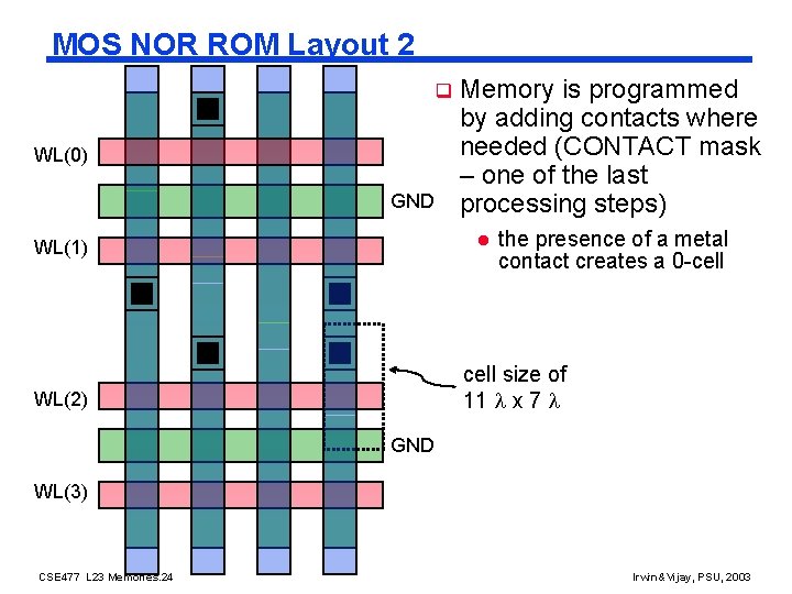
MOS NOR ROM Layout 2 q WL(0) GND Memory is programmed by adding contacts where needed (CONTACT mask – one of the last processing steps) l WL(1) the presence of a metal contact creates a 0 -cell size of 11 x 7 WL(2) GND WL(3) CSE 477 L 23 Memories. 24 Irwin&Vijay, PSU, 2003

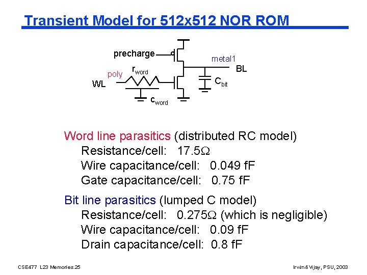
Transient Model for 512 x 512 NOR ROM precharge poly metal 1 rword BL Cbit WL cword Word line parasitics (distributed RC model) Resistance/cell: 17. 5 Wire capacitance/cell: 0. 049 f. F Gate capacitance/cell: 0. 75 f. F Bit line parasitics (lumped C model) Resistance/cell: 0. 275 (which is negligible) Wire capacitance/cell: 0. 09 f. F Drain capacitance/cell: 0. 8 f. F CSE 477 L 23 Memories. 25 Irwin&Vijay, PSU, 2003

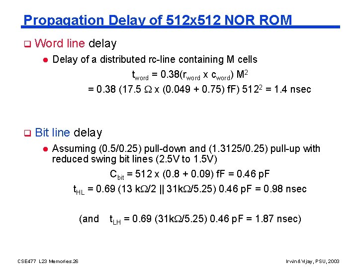
Propagation Delay of 512 x 512 NOR ROM q Word line delay l q Delay of a distributed rc-line containing M cells tword = 0. 38(rword x cword) M 2 = 0. 38 (17. 5 x (0. 049 + 0. 75) f. F) 5122 = 1. 4 nsec Bit line delay l Assuming (0. 5/0. 25) pull-down and (1. 3125/0. 25) pull-up with reduced swing bit lines (2. 5 V to 1. 5 V) Cbit = 512 x (0. 8 + 0. 09) f. F = 0. 46 p. F t. HL = 0. 69 (13 k /2 || 31 k /5. 25) 0. 46 p. F = 0. 98 nsec (and CSE 477 L 23 Memories. 26 t. LH = 0. 69 (31 k /5. 25) 0. 46 p. F = 1. 87 nsec) Irwin&Vijay, PSU, 2003

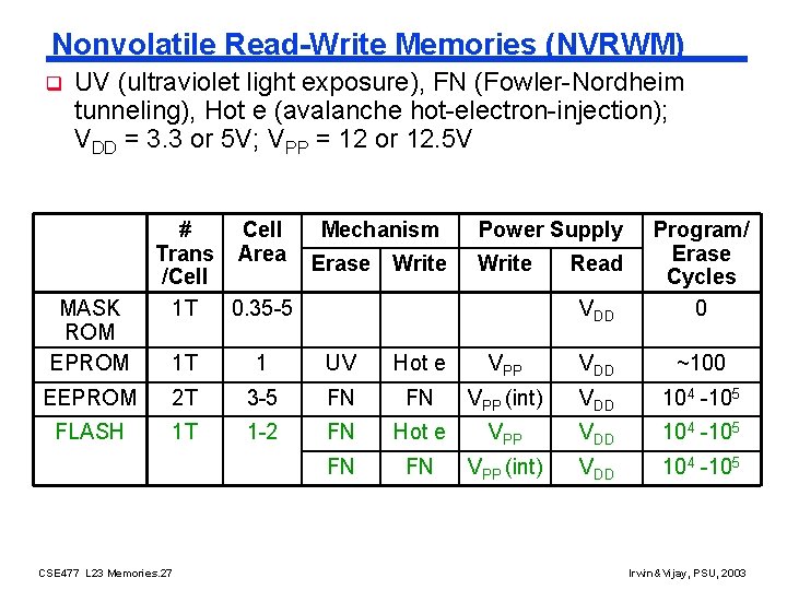
Nonvolatile Read-Write Memories (NVRWM) q UV (ultraviolet light exposure), FN (Fowler-Nordheim tunneling), Hot e (avalanche hot-electron-injection); VDD = 3. 3 or 5 V; VPP = 12 or 12. 5 V MASK ROM EPROM # Cell Mechanism Trans Area Erase Write /Cell 1 T 0. 35 -5 Power Supply Write VDD Program/ Erase Cycles 0 Read 1 T 1 UV Hot e VPP VDD ~100 EEPROM 2 T 3 -5 FN FN VPP (int) VDD 104 -105 FLASH 1 T 1 -2 FN Hot e VPP VDD 104 -105 FN FN VPP (int) VDD 104 -105 CSE 477 L 23 Memories. 27 Irwin&Vijay, PSU, 2003

Next Lecture and Reminders q Next lecture l SRAM, DRAM, and CAM cores - Reading assignment – Rabaey, et al, 12. 2. 3 -12. 2. 4 q Reminders l HW#5 will (optional) due December 2 nd l Project final reports due December 4 th l Final grading negotiations/correction (except for the final exam) must be concluded by December 10 th Final exam scheduled l - Tuesday, December 16 th from 10: 10 to noon in 118 and 113 Thomas CSE 477 L 23 Memories. 28 Irwin&Vijay, PSU, 2003