CSE 477 VLSI Digital Circuits Fall 2003 Lecture
![Scan Path Testing A B REG[1] REG[0] REG[2] SCANIN REG[3] REG[4] COMPIN COMP REG[5] Scan Path Testing A B REG[1] REG[0] REG[2] SCANIN REG[3] REG[4] COMPIN COMP REG[5]](https://slidetodoc.com/presentation_image/2ff2f9f92d79e918b917453479bc386f/image-16.jpg)
- Slides: 25

CSE 477 VLSI Digital Circuits Fall 2003 Lecture 28: Design for Test Mary Jane Irwin ( www. cse. psu. edu/~mji ) www. cse. psu. edu/~cg 477 [Adapted from Rabaey’s Digital Integrated Circuits, Second Edition, © 2003 Rabaey, A. Chandrakasan, B. Nikolic] CSE 477 L 28 DFT. 1 J. Irwin&Vijay, PSU, 2003

Test Procedures q Diagnostic test l l q q used in debugging and defect localization can afford to spend time testing Production test - “go/no go” l used in chip production (wafer and/or packaged) l since have to test each part, must be fast Parametric test l l l [v, i] versus [0, 1] check parameters such as noise margins, Vt, tp at corners (range of temperatures and supply voltage variations) usually done with special wafer drop-ins CSE 477 L 28 DFT. 2 Irwin&Vijay, PSU, 2003

Testing Fabricated Designs q Goals of design-for-test (DFT) l q DFT mantra l q make testing of manufactured parts swift and comprehensive Provide controllability and observability Components of DFT strategy l l Provide test patterns that guarantee reasonable coverage Provide circuitry to enable testing CSE 477 L 28 DFT. 3 Irwin&Vijay, PSU, 2003

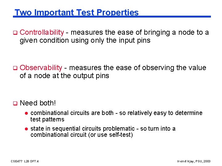
Two Important Test Properties q Controllability - measures the ease of bringing a node to a given condition using only the input pins q Observability - measures the ease of observing the value of a node at the output pins q Need both! l l combinational circuits are both - so relatively easy to determine test patterns state in sequential circuits problematic - so turn into a combinational circuit (or use self-test) CSE 477 L 28 DFT. 4 Irwin&Vijay, PSU, 2003

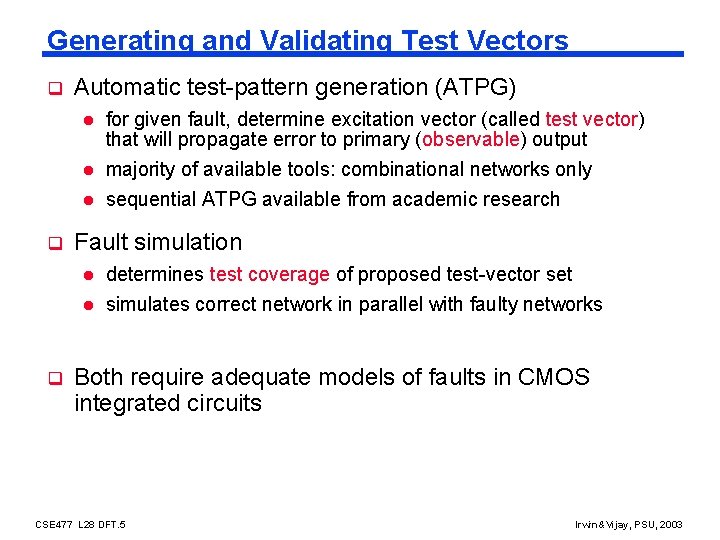
Generating and Validating Test Vectors q Automatic test-pattern generation (ATPG) l for given fault, determine excitation vector (called test vector) that will propagate error to primary (observable) output majority of available tools: combinational networks only l sequential ATPG available from academic research l q q Fault simulation l determines test coverage of proposed test-vector set l simulates correct network in parallel with faulty networks Both require adequate models of faults in CMOS integrated circuits CSE 477 L 28 DFT. 5 Irwin&Vijay, PSU, 2003

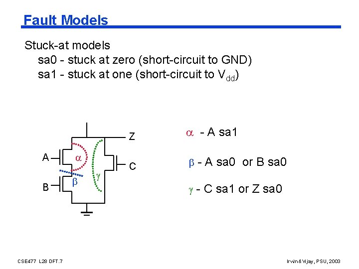
Fault Models Stuck-at models sa 0 - stuck at zero (short-circuit to GND) sa 1 - stuck at one (short-circuit to Vdd) A B CSE 477 L 28 DFT. 7 Z - A sa 1 C - A sa 0 or B sa 0 - C sa 1 or Z sa 0 Irwin&Vijay, PSU, 2003

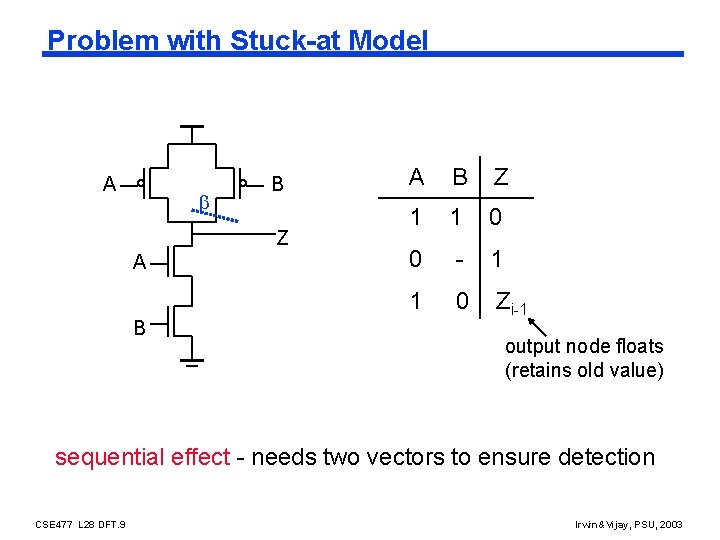
Problem with Stuck-at Model A B Z 1 1 0 0 - 1 1 0 Zi-1 output node floats (retains old value) sequential effect - needs two vectors to ensure detection CSE 477 L 28 DFT. 9 Irwin&Vijay, PSU, 2003

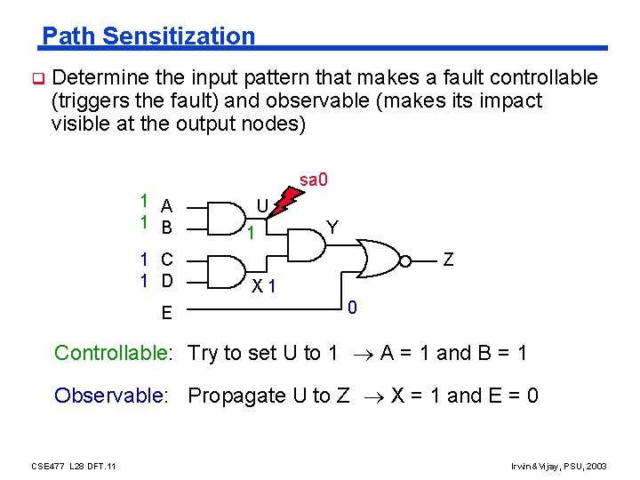
Path Sensitization q Determine the input pattern that makes a fault controllable (triggers the fault) and observable (makes its impact visible at the output nodes) sa 0 1 A 1 B 1 C 1 D E U 1 Y Z X 1 0 Controllable: Try to set U to 1 A = 1 and B = 1 Observable: Propagate U to Z X = 1 and E = 0 CSE 477 L 28 DFT. 11 Irwin&Vijay, PSU, 2003

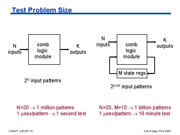
Test Problem Size comb logic module N inputs K outputs comb logic module M state regs 2 N input patterns 2 N+M input patterns N=20 1 million patterns 1 sec/pattern 1 second test CSE 477 L 28 DFT. 13 N=20, M=10 1 billion patterns 1 sec/pattern 16 minute test Irwin&Vijay, PSU, 2003

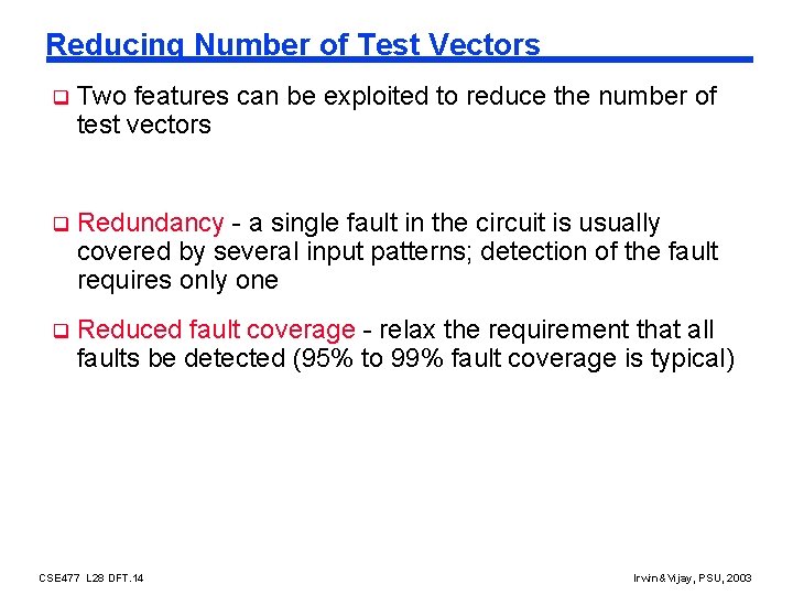
Reducing Number of Test Vectors q Two features can be exploited to reduce the number of test vectors q Redundancy - a single fault in the circuit is usually covered by several input patterns; detection of the fault requires only one q Reduced fault coverage - relax the requirement that all faults be detected (95% to 99% fault coverage is typical) CSE 477 L 28 DFT. 14 Irwin&Vijay, PSU, 2003

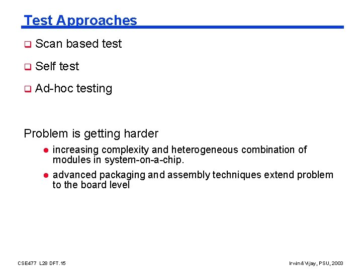
Test Approaches q Scan based test q Self test q Ad-hoc testing Problem is getting harder l l increasing complexity and heterogeneous combination of modules in system-on-a-chip. advanced packaging and assembly techniques extend problem to the board level CSE 477 L 28 DFT. 15 Irwin&Vijay, PSU, 2003

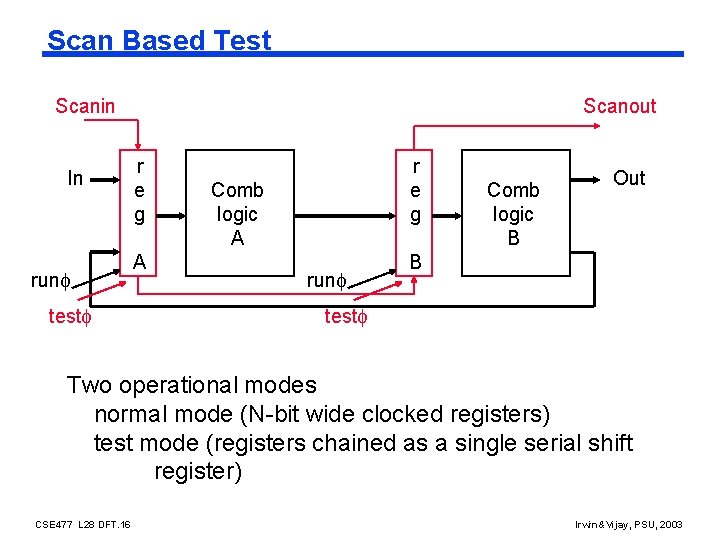
Scan Based Test Scanin In run test Scanout r e g A r e g Comb logic A run Comb logic B Out B test Two operational modes normal mode (N-bit wide clocked registers) test mode (registers chained as a single serial shift register) CSE 477 L 28 DFT. 16 Irwin&Vijay, PSU, 2003

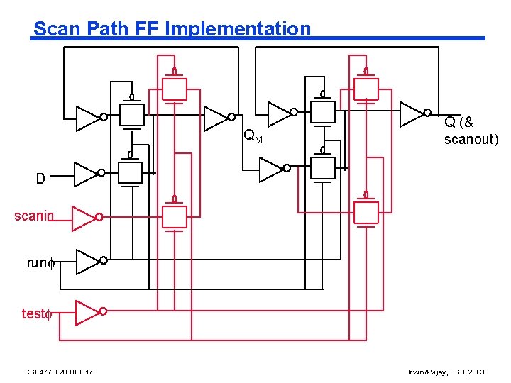
Scan Path FF Implementation QM Q (& scanout) D scanin run test CSE 477 L 28 DFT. 17 Irwin&Vijay, PSU, 2003

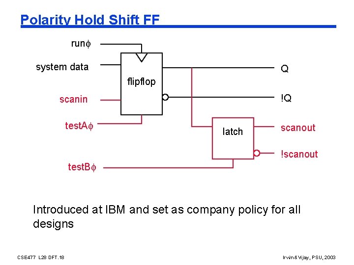
Polarity Hold Shift FF run system data Q flipflop !Q scanin test. A latch scanout !scanout test. B Introduced at IBM and set as company policy for all designs CSE 477 L 28 DFT. 18 Irwin&Vijay, PSU, 2003

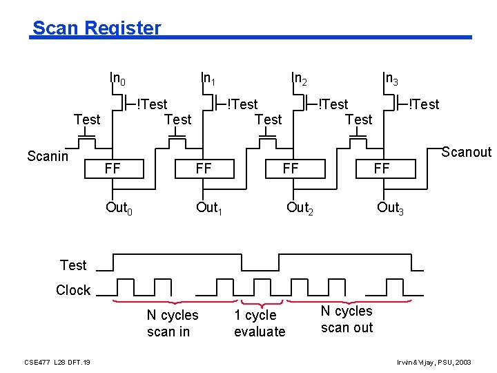
Scan Register In 0 !Test Scanin In 1 In 2 !Test In 3 !Test Scanout FF FF Out 0 Out 1 Out 2 Out 3 Test Clock N cycles scan in CSE 477 L 28 DFT. 19 1 cycle evaluate N cycles scan out Irwin&Vijay, PSU, 2003
![Scan Path Testing A B REG1 REG0 REG2 SCANIN REG3 REG4 COMPIN COMP REG5 Scan Path Testing A B REG[1] REG[0] REG[2] SCANIN REG[3] REG[4] COMPIN COMP REG[5]](https://slidetodoc.com/presentation_image/2ff2f9f92d79e918b917453479bc386f/image-16.jpg)
Scan Path Testing A B REG[1] REG[0] REG[2] SCANIN REG[3] REG[4] COMPIN COMP REG[5] SCANOUT Partial scan be more effective for pipelined datapaths CSE 477 L 28 DFT. 20 Irwin&Vijay, PSU, 2003

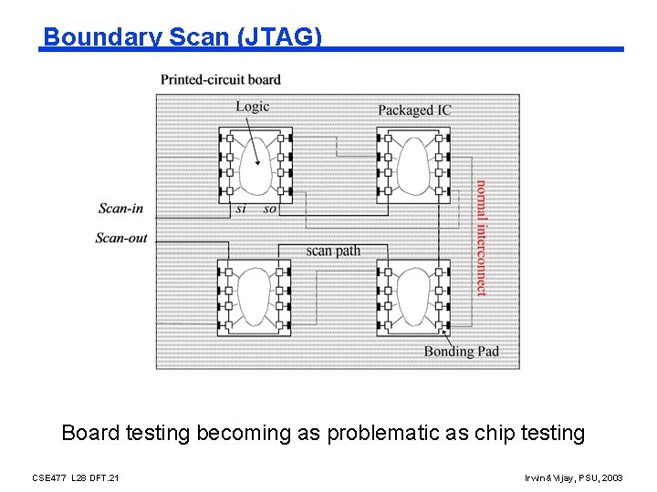
Boundary Scan (JTAG) Board testing becoming as problematic as chip testing CSE 477 L 28 DFT. 21 Irwin&Vijay, PSU, 2003

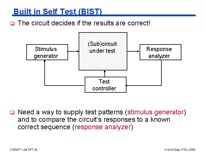
Built in Self Test (BIST) q The circuit decides if the results are correct! Stimulus generator (Sub)circuit under test Response analyzer Test controller q Need a way to supply test patterns (stimulus generator) and to compare the circuit’s responses to a known correct sequence (response analyzer) CSE 477 L 28 DFT. 22 Irwin&Vijay, PSU, 2003

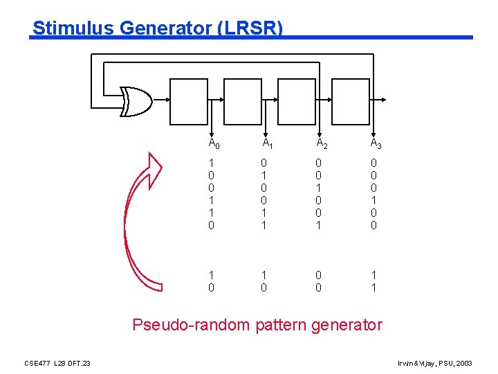
Stimulus Generator (LRSR) A 0 A 1 A 2 A 3 1 0 0 1 0 0 0 1 0 1 0 0 0 1 1 Pseudo-random pattern generator CSE 477 L 28 DFT. 23 Irwin&Vijay, PSU, 2003

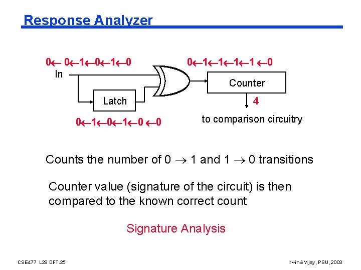
Response Analyzer 0 0 1 0 In 0 1 1 0 Counter Latch 0 1 0 0 4 to comparison circuitry Counts the number of 0 1 and 1 0 transitions Counter value (signature of the circuit) is then compared to the known correct count Signature Analysis CSE 477 L 28 DFT. 25 Irwin&Vijay, PSU, 2003

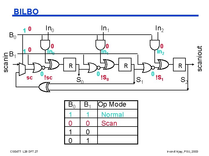
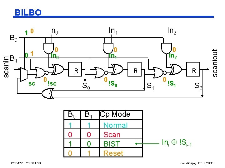
B 0 scanin B 1 10 In 1 In 2 10 0 In 1 0 In 2 R sc 0 !sc S 0 B 0 1 0 CSE 477 L 28 DFT. 27 R 0 !S 0 R S 1 0 !S 1 scaniout BILBO S 2 B 1 Op Mode 1 Normal 0 Scan 0 1 Irwin&Vijay, PSU, 2003

B 0 scanin B 1 10 In 1 In 2 01 0 In 0 0 In 1 0 In 2 R sc 0 !sc S 0 B 0 1 0 CSE 477 L 28 DFT. 28 R 0 !S 0 B 1 Op Mode 1 Normal 0 Scan 0 BIST 1 Reset R S 1 0 !S 1 scaniout BILBO S 2 Ini !Si-1 Irwin&Vijay, PSU, 2003

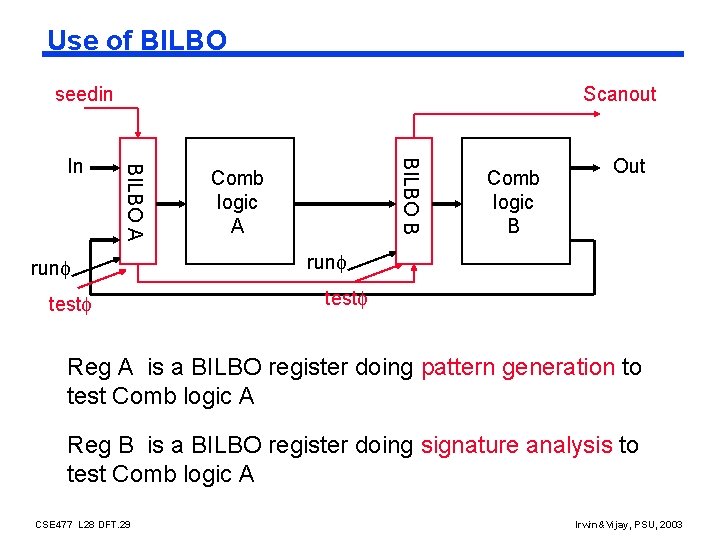
Use of BILBO seedin run test BILBO B BILBO A In Scanout Comb logic A Comb logic B Out run test Reg A is a BILBO register doing pattern generation to test Comb logic A Reg B is a BILBO register doing signature analysis to test Comb logic A CSE 477 L 28 DFT. 29 Irwin&Vijay, PSU, 2003

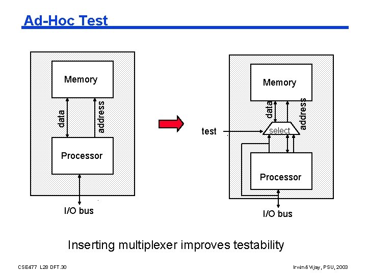
Ad-Hoc Test test select address Memory data address Memory Processor I/O bus Inserting multiplexer improves testability CSE 477 L 28 DFT. 30 Irwin&Vijay, PSU, 2003

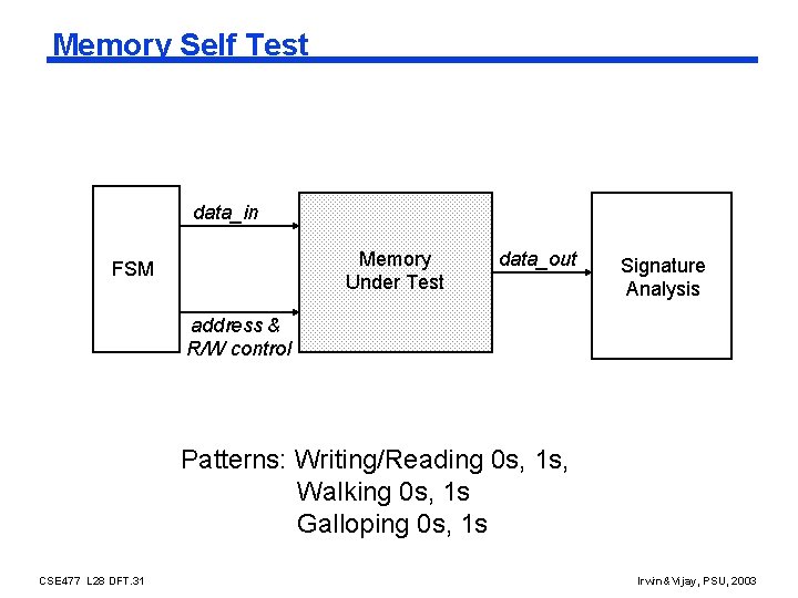
Memory Self Test data_in Memory Under Test FSM data_out Signature Analysis address & R/W control Patterns: Writing/Reading 0 s, 1 s, Walking 0 s, 1 s Galloping 0 s, 1 s CSE 477 L 28 DFT. 31 Irwin&Vijay, PSU, 2003