CSE 477 VLSI Digital Circuits Fall 2003 Lecture
- Slides: 30

CSE 477 VLSI Digital Circuits Fall 2003 Lecture 08: MOS & Wire Capacitances Mary Jane Irwin ( www. cse. psu. edu/~mji ) www. cse. psu. edu/~cg 477 [Adapted from Rabaey’s Digital Integrated Circuits, Second Edition, © 2003 Rabaey, A. Chandrakasan, B. Nikolic] CSE 477 L 08 Capacitance. 1 J. Irwin&Vijay, PSU, 2003

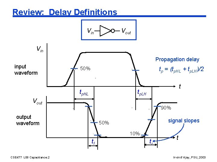
Review: Delay Definitions Vin Vout Vin Propagation delay input waveform 50% tp = (tp. HL + tp. LH)/2 tp. HL t tp. LH Vout 90% output waveform signal slopes 50% 10% tf CSE 477 L 08 Capacitance. 2 tr t Irwin&Vijay, PSU, 2003

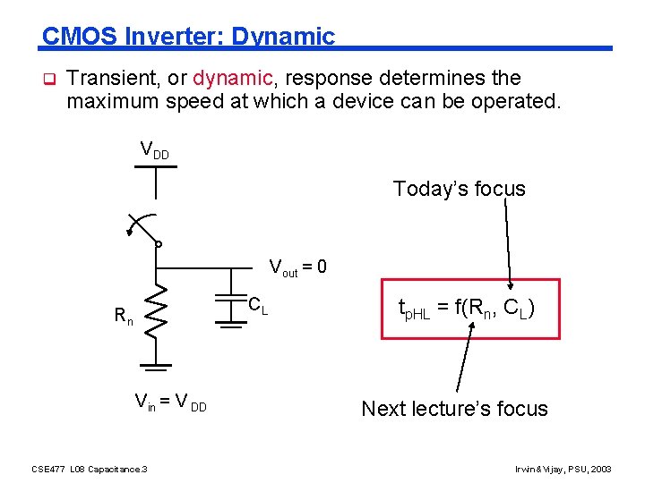
CMOS Inverter: Dynamic q Transient, or dynamic, response determines the maximum speed at which a device can be operated. VDD Today’s focus Vout = 0 CL Rn Vin = V DD CSE 477 L 08 Capacitance. 3 tp. HL = f(Rn, CL) Next lecture’s focus Irwin&Vijay, PSU, 2003

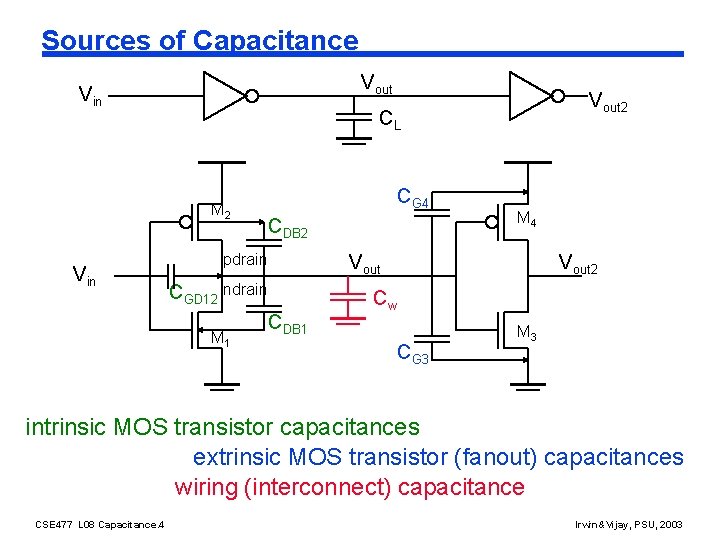
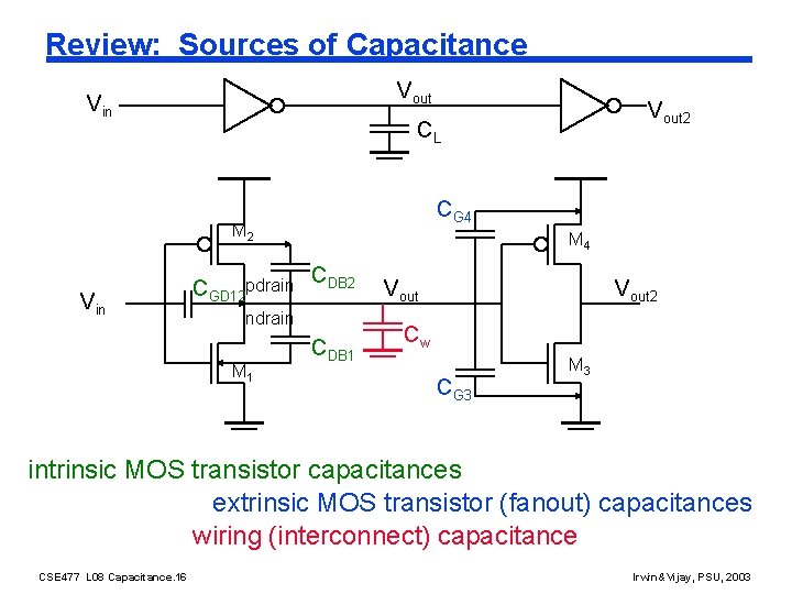
Sources of Capacitance Vout Vin CL M 2 Vin Vout 2 CG 4 CDB 2 pdrain Vout CGD 12 ndrain M 1 M 4 CDB 1 Vout 2 Cw CG 3 M 3 intrinsic MOS transistor capacitances extrinsic MOS transistor (fanout) capacitances wiring (interconnect) capacitance CSE 477 L 08 Capacitance. 4 Irwin&Vijay, PSU, 2003

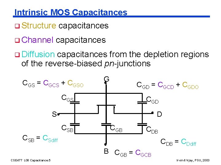
Intrinsic MOS Capacitances q Structure q Channel capacitances q Diffusion capacitances from the depletion regions of the reverse-biased pn-junctions CGS = CGCS + CGSO G CGD = CGCD + CGDO CGS CGD S D CSB = CSdiff CGB CDB = CDdiff B CGB = CGCB CSE 477 L 08 Capacitance. 5 Irwin&Vijay, PSU, 2003

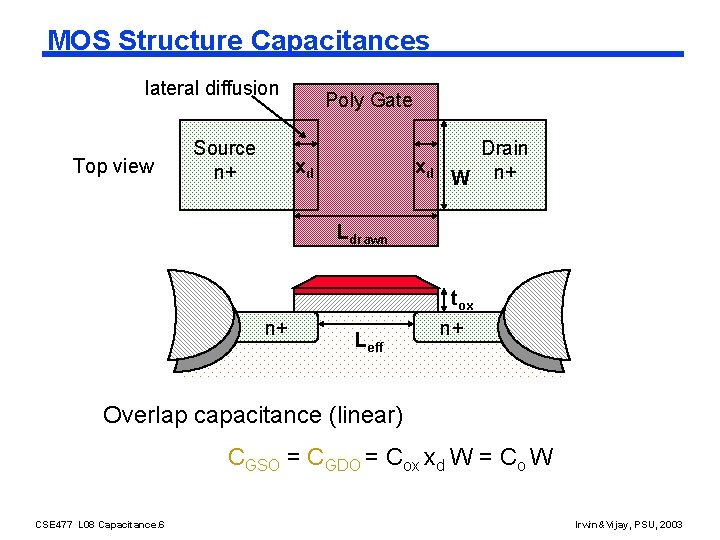
MOS Structure Capacitances lateral diffusion Top view Source n+ Poly Gate xd xd Drain W n+ Ldrawn n+ Leff tox n+ Overlap capacitance (linear) CGSO = CGDO = Cox xd W = Co W CSE 477 L 08 Capacitance. 6 Irwin&Vijay, PSU, 2003

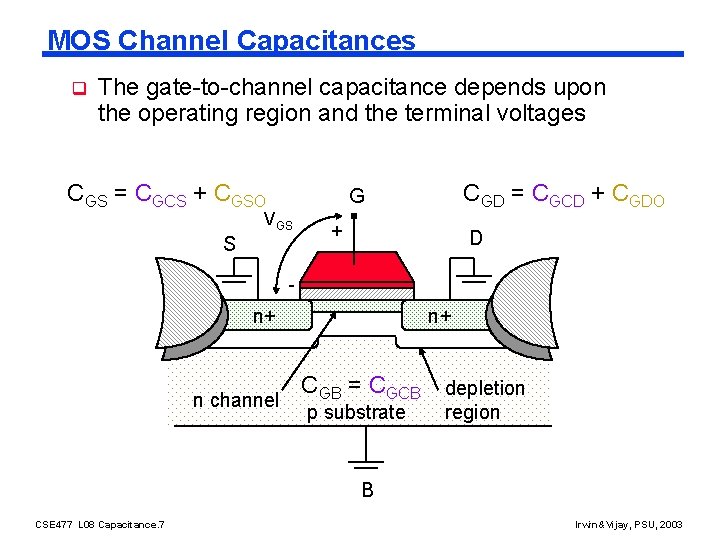
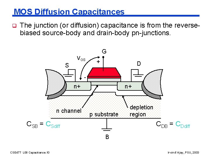
MOS Channel Capacitances q The gate-to-channel capacitance depends upon the operating region and the terminal voltages CGS = CGCS + CGSO CGD = CGCD + CGDO G VGS S + D - n+ n+ n channel CGB = CGCB p substrate depletion region B CSE 477 L 08 Capacitance. 7 Irwin&Vijay, PSU, 2003

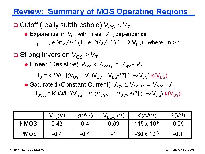
Review: Summary of MOS Operating Regions q Cutoff (really subthreshold) VGS VT l q Exponential in VGS with linear VDS dependence ID = IS e (q. VGS/nk. T) (1 - e -(q. VDS/k. T) ) (1 - VDS) where n 1 Strong Inversion VGS > VT l Linear (Resistive) VDS < VDSAT = VGS - VT ID = k’ W/L [(VGS – VT)VDS – VDS 2/2] (1+ VDS) (VDS) l Saturated (Constant Current) VDSAT = VGS - VT IDSat = k’ W/L [(VGS – VT)VDSAT – VDSAT 2/2] (1+ VDS) (VDS) NMOS VT 0(V) 0. 43 (V 0. 5) 0. 4 VDSAT(V) 0. 63 k’(A/V 2) 115 x 10 -6 (V-1) 0. 06 PMOS -0. 4 -1 -30 x 10 -6 -0. 1 CSE 477 L 08 Capacitance. 8 Irwin&Vijay, PSU, 2003

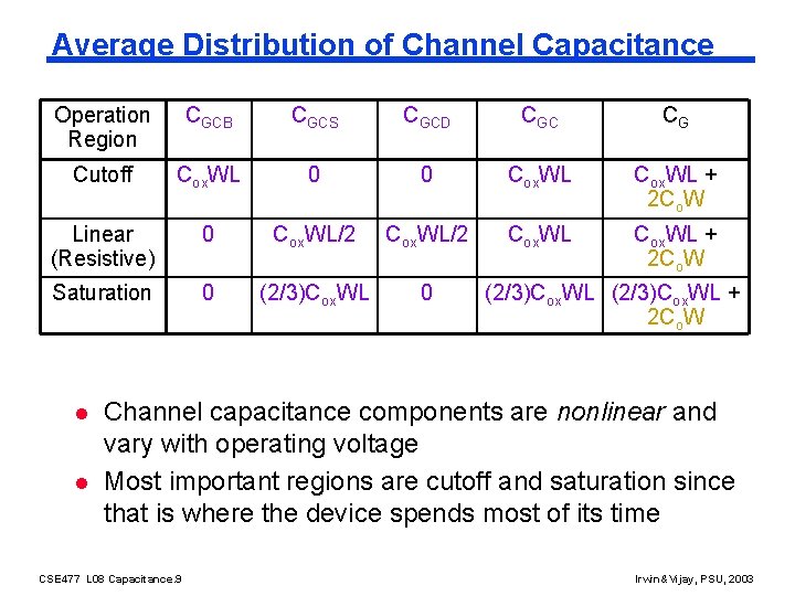
Average Distribution of Channel Capacitance Operation Region CGCB CGCS CGCD CGC CG Cutoff Cox. WL 0 0 Cox. WL + 2 Co. W Linear (Resistive) 0 Cox. WL/2 Cox. WL + 2 Co. W Saturation 0 (2/3)Cox. WL 0 l l (2/3)Cox. WL + 2 Co. W Channel capacitance components are nonlinear and vary with operating voltage Most important regions are cutoff and saturation since that is where the device spends most of its time CSE 477 L 08 Capacitance. 9 Irwin&Vijay, PSU, 2003

MOS Diffusion Capacitances q The junction (or diffusion) capacitance is from the reversebiased source-body and drain-body pn-junctions. G VGS S + D - n+ n+ n channel p substrate CSB = CSdiff depletion region CDB = CDdiff B CSE 477 L 08 Capacitance. 10 Irwin&Vijay, PSU, 2003

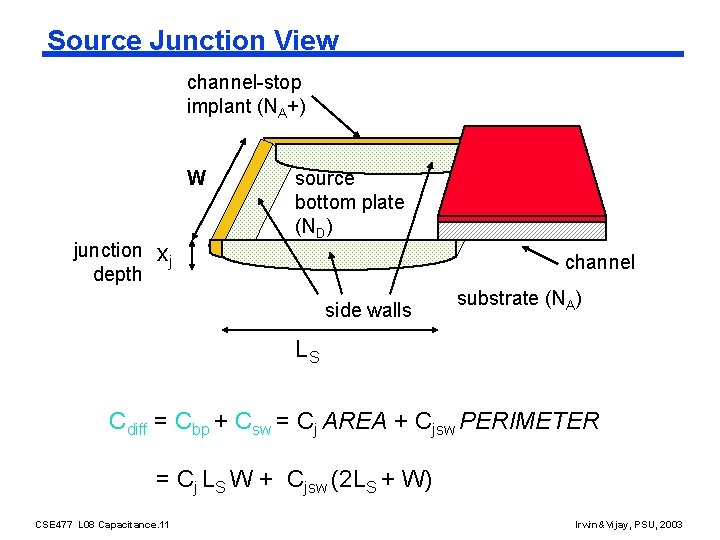
Source Junction View channel-stop implant (NA+) W junction depth xj source bottom plate (ND) channel side walls substrate (NA) LS Cdiff = Cbp + Csw = Cj AREA + Cjsw PERIMETER = Cj LS W + Cjsw (2 LS + W) CSE 477 L 08 Capacitance. 11 Irwin&Vijay, PSU, 2003

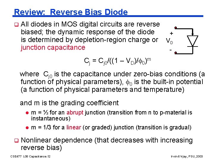
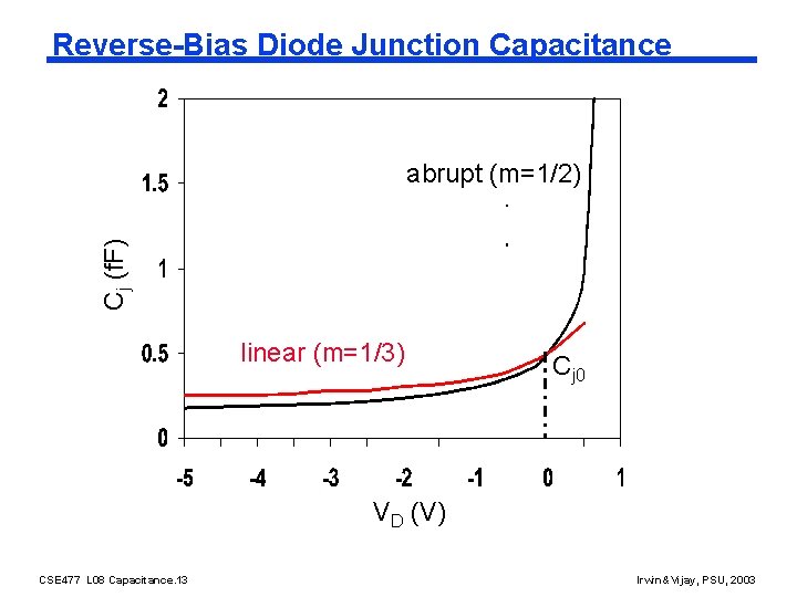
Review: Reverse Bias Diode q All diodes in MOS digital circuits are reverse biased; the dynamic response of the diode + is determined by depletion-region charge or VD junction capacitance Cj = Cj 0/((1 – VD)/ 0)m where Cj 0 is the capacitance under zero-bias conditions (a function of physical parameters), 0 is the built-in potential (a function of physical parameters and temperature) and m is the grading coefficient l l q m = ½ for an abrupt junction (transition from n to p-material is instantaneous) m = 1/3 for a linear (or graded) junction (transition is gradual) Nonlinear dependence (that decreases with increasing reverse bias) CSE 477 L 08 Capacitance. 12 Irwin&Vijay, PSU, 2003

Reverse-Bias Diode Junction Capacitance Cj (f. F) abrupt (m=1/2) linear (m=1/3) Cj 0 VD (V) CSE 477 L 08 Capacitance. 13 Irwin&Vijay, PSU, 2003

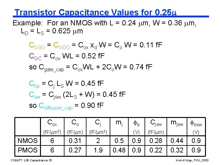
Transistor Capacitance Values for 0. 25 Example: For an NMOS with L = 0. 24 m, W = 0. 36 m, LD = LS = 0. 625 m CGSO = CGDO = Cox xd W = Co W = 0. 11 f. F CGC = Cox WL = 0. 52 f. F so Cgate_cap = Cox. WL + 2 Co. W = 0. 74 f. F Cbp = Cj LS W = 0. 45 f. F Csw = Cjsw (2 LS + W) = 0. 45 f. F so Cdiffusion_cap = 0. 90 f. F NMOS PMOS Cox Co Cj (f. F/ m 2) 6 6 0. 31 0. 27 2 1. 9 CSE 477 L 08 Capacitance. 15 b Cjsw (V) (f. F/ m) 0. 5 0. 9 0. 48 0. 9 0. 28 0. 22 mj mjsw bsw (V) 0. 44 0. 32 0. 9 Irwin&Vijay, PSU, 2003

Review: Sources of Capacitance Vout Vin CL CG 4 M 2 Vin Vout 2 CGD 12 pdrain M 4 CDB 2 ndrain M 1 CDB 1 Vout 2 Cw CG 3 M 3 intrinsic MOS transistor capacitances extrinsic MOS transistor (fanout) capacitances wiring (interconnect) capacitance CSE 477 L 08 Capacitance. 16 Irwin&Vijay, PSU, 2003

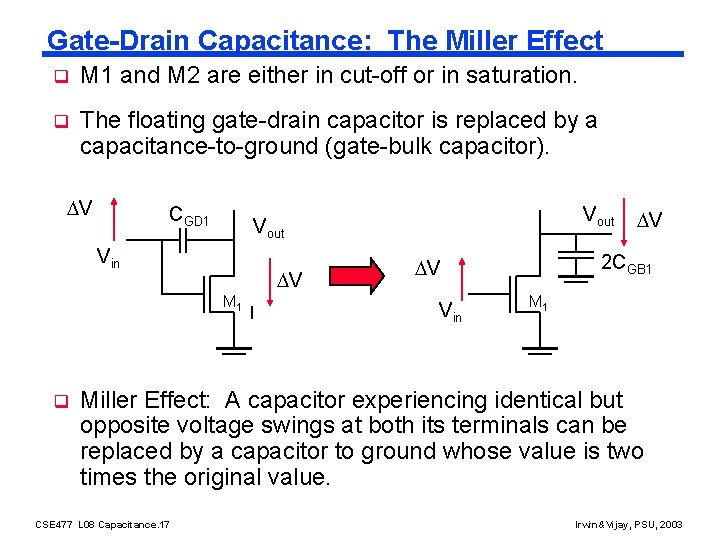
Gate-Drain Capacitance: The Miller Effect q M 1 and M 2 are either in cut-off or in saturation. q The floating gate-drain capacitor is replaced by a capacitance-to-ground (gate-bulk capacitor). V CGD 1 Vin V M 1 q Vout 2 CGB 1 V Vin V M 1 Miller Effect: A capacitor experiencing identical but opposite voltage swings at both its terminals can be replaced by a capacitor to ground whose value is two times the original value. CSE 477 L 08 Capacitance. 17 Irwin&Vijay, PSU, 2003

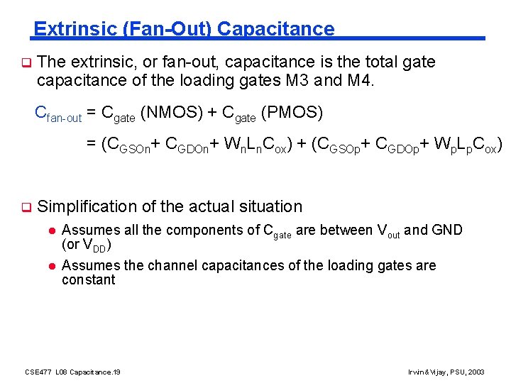
Extrinsic (Fan-Out) Capacitance q The extrinsic, or fan-out, capacitance is the total gate capacitance of the loading gates M 3 and M 4. Cfan-out = Cgate (NMOS) + Cgate (PMOS) = (CGSOn+ CGDOn+ Wn. Ln. Cox) + (CGSOp+ CGDOp+ Wp. Lp. Cox) q Simplification of the actual situation l l Assumes all the components of Cgate are between Vout and GND (or VDD) Assumes the channel capacitances of the loading gates are constant CSE 477 L 08 Capacitance. 19 Irwin&Vijay, PSU, 2003

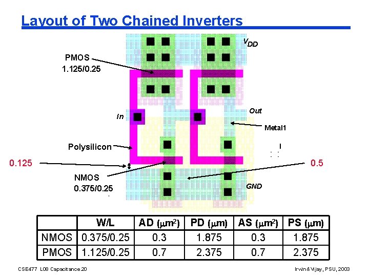
Layout of Two Chained Inverters VDD PMOS 1. 125/0. 25 1. 2 m =2 l Out In Metal 1 Polysilicon 0. 125 0. 5 NMOS 0. 375/0. 25 W/L AD ( m 2) NMOS 0. 375/0. 25 0. 3 PMOS 1. 125/0. 25 0. 7 CSE 477 L 08 Capacitance. 20 GND PD ( m) 1. 875 2. 375 AS ( m 2) PS ( m) 0. 3 1. 875 0. 7 2. 375 Irwin&Vijay, PSU, 2003

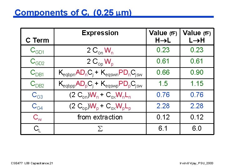
Components of CL (0. 25 m) C Term CGD 1 Expression 2 C on W n Value (f. F) H L L H 0. 23 CGD 2 2 C op W p 0. 61 CDB 1 Keqbpn. ADn. Cj + Keqswn. PDn. Cjsw 0. 66 0. 90 CDB 2 Keqbpp. ADp. Cj + Keqswp. PDp. Cjsw 1. 5 1. 15 CG 3 (2 Con)Wn + Cox. Wn. Ln 0. 76 CG 4 (2 Cop)Wp + Cox. Wp. Lp 2. 28 Cw from extraction 0. 12 CL 6. 1 6. 0 CSE 477 L 08 Capacitance. 21 Irwin&Vijay, PSU, 2003

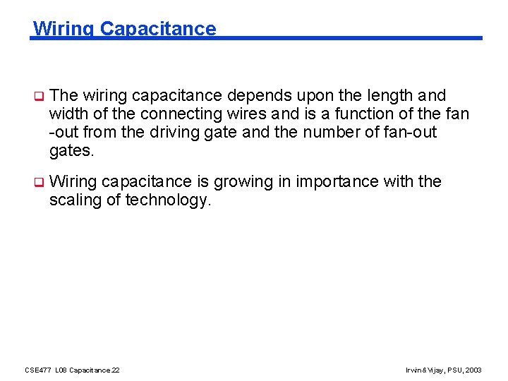
Wiring Capacitance q The wiring capacitance depends upon the length and width of the connecting wires and is a function of the fan -out from the driving gate and the number of fan-out gates. q Wiring capacitance is growing in importance with the scaling of technology. CSE 477 L 08 Capacitance. 22 Irwin&Vijay, PSU, 2003

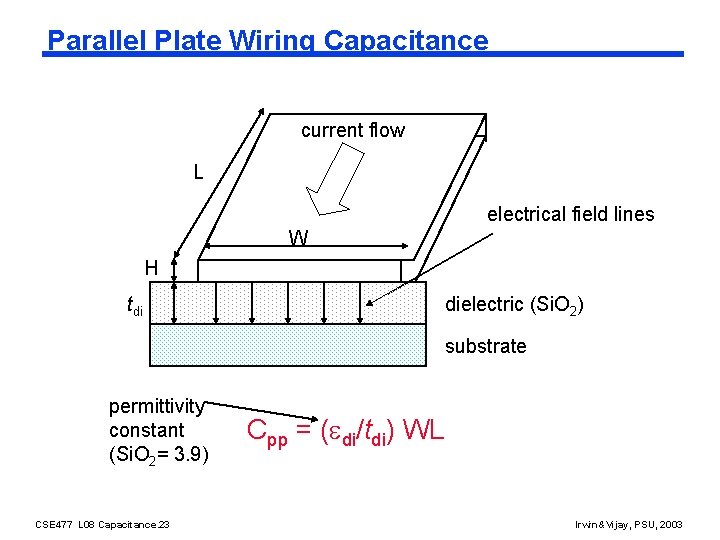
Parallel Plate Wiring Capacitance current flow L electrical field lines W H tdi dielectric (Si. O 2) substrate permittivity constant (Si. O 2= 3. 9) CSE 477 L 08 Capacitance. 23 Cpp = ( di/tdi) WL Irwin&Vijay, PSU, 2003

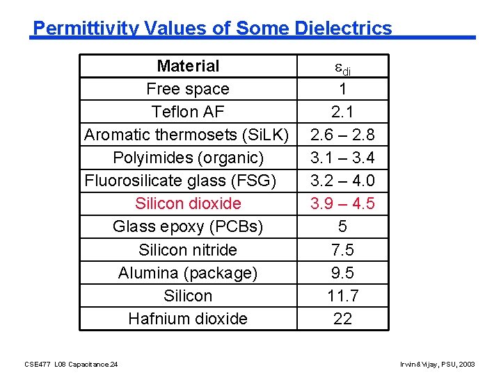
Permittivity Values of Some Dielectrics Material Free space Teflon AF Aromatic thermosets (Si. LK) Polyimides (organic) Fluorosilicate glass (FSG) Silicon dioxide Glass epoxy (PCBs) Silicon nitride Alumina (package) Silicon Hafnium dioxide CSE 477 L 08 Capacitance. 24 di 1 2. 6 – 2. 8 3. 1 – 3. 4 3. 2 – 4. 0 3. 9 – 4. 5 5 7. 5 9. 5 11. 7 22 Irwin&Vijay, PSU, 2003

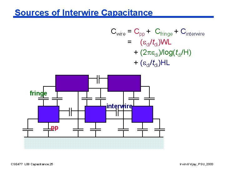
Sources of Interwire Capacitance Cwire = Cpp + Cfringe + Cinterwire = ( di/tdi)WL + (2 di)/log(tdi/H) + ( di/tdi)HL fringe interwire pp CSE 477 L 08 Capacitance. 25 Irwin&Vijay, PSU, 2003

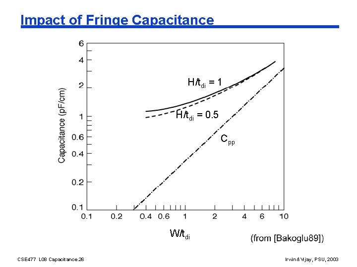
Impact of Fringe Capacitance H/tdi = 1 H/tdi = 0. 5 Cpp W/tdi CSE 477 L 08 Capacitance. 26 Irwin&Vijay, PSU, 2003

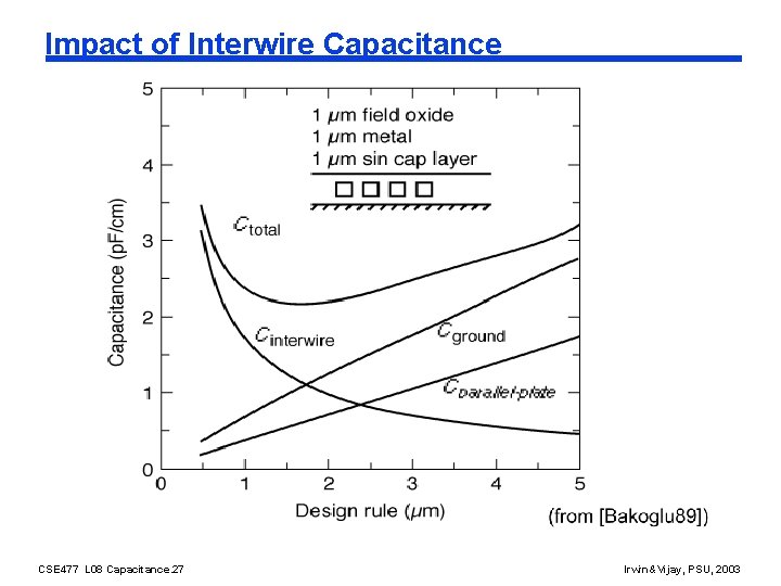
Impact of Interwire Capacitance CSE 477 L 08 Capacitance. 27 Irwin&Vijay, PSU, 2003

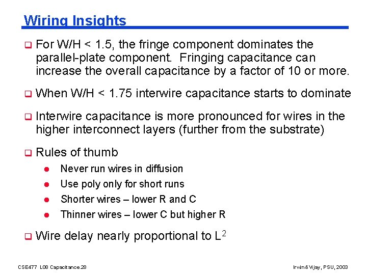
Wiring Insights q For W/H < 1. 5, the fringe component dominates the parallel-plate component. Fringing capacitance can increase the overall capacitance by a factor of 10 or more. q When W/H < 1. 75 interwire capacitance starts to dominate q Interwire capacitance is more pronounced for wires in the higher interconnect layers (further from the substrate) q Rules of thumb l l q Never run wires in diffusion Use poly only for short runs Shorter wires – lower R and C Thinner wires – lower C but higher R Wire delay nearly proportional to L 2 CSE 477 L 08 Capacitance. 28 Irwin&Vijay, PSU, 2003

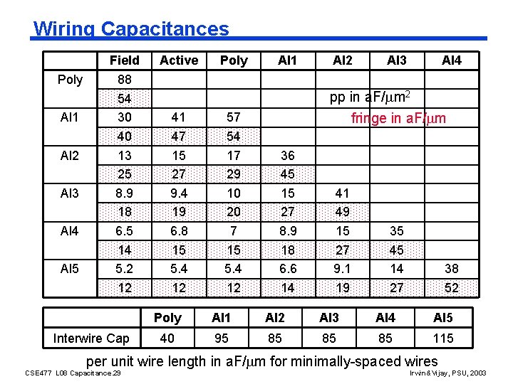
Wiring Capacitances Poly Al 1 Al 2 Al 3 Al 4 Al 5 Field 88 54 30 40 13 25 8. 9 18 6. 5 14 5. 2 12 Interwire Cap Active Poly Al 1 Al 2 Al 3 Al 4 pp in a. F/ m 2 41 47 15 27 9. 4 19 6. 8 15 5. 4 12 57 54 17 29 10 20 7 15 5. 4 12 fringe in a. F/ m 36 45 15 27 8. 9 18 6. 6 14 41 49 15 27 9. 1 19 35 45 14 27 38 52 Poly Al 1 Al 2 Al 3 Al 4 Al 5 40 95 85 85 85 115 per unit wire length in a. F/ m for minimally-spaced wires CSE 477 L 08 Capacitance. 29 Irwin&Vijay, PSU, 2003

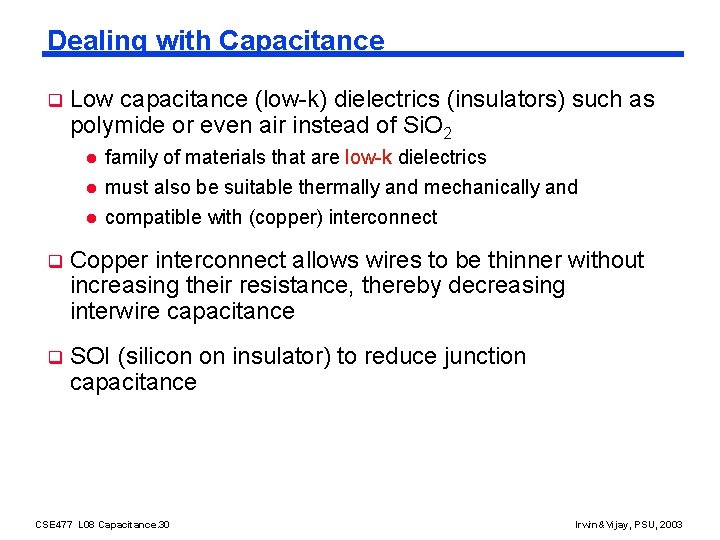
Dealing with Capacitance q Low capacitance (low-k) dielectrics (insulators) such as polymide or even air instead of Si. O 2 l family of materials that are low-k dielectrics must also be suitable thermally and mechanically and l compatible with (copper) interconnect l q Copper interconnect allows wires to be thinner without increasing their resistance, thereby decreasing interwire capacitance q SOI (silicon on insulator) to reduce junction capacitance CSE 477 L 08 Capacitance. 30 Irwin&Vijay, PSU, 2003

Next Time: Dealing with Resistance q MOS structure resistance - Ron q Wiring resistance q Contact resistance CSE 477 L 08 Capacitance. 31 Irwin&Vijay, PSU, 2003

Next Lecture and Reminders q Next lecture l MOS resistance - Reading assignment – Rabaey, et al, 4. 3. 2, 4. 4. 1 -4. 4. 4 - Another lecture given by guest lecturer Greg Link q Reminders l HW#2 due today l Project specs due (on-line) October 9 th l HW#3 due October 16 th HW#4 due November 11 th (not Nov 4 th as on outline) HW#5 will be optional (due November 20 th) Evening midterm exam scheduled l l l - Monday, October 20 th , 20: 15 to 22: 15, Location TBD - Only one midterm conflict scheduled CSE 477 L 08 Capacitance. 32 Irwin&Vijay, PSU, 2003