CSE 477 VLSI Digital Circuits Fall 2003 Lecture
- Slides: 23

CSE 477 VLSI Digital Circuits Fall 2003 Lecture 04: CMOS Inverter (static view) Mary Jane Irwin ( www. cse. psu. edu/~mji ) www. cse. psu. edu/~cg 477 [Adapted from Rabaey’s Digital Integrated Circuits, Second Edition, © 2003 Rabaey, A. Chandrakasan, B. Nikolic] CSE 477 L 04 CMOS Inverter. 1 J. Irwin&Vijay, PSU, 2003

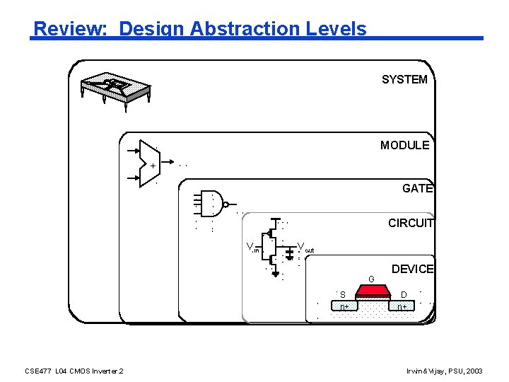
Review: Design Abstraction Levels SYSTEM MODULE + GATE CIRCUIT Vin Vout G S n+ CSE 477 L 04 CMOS Inverter. 2 DEVICE D n+ Irwin&Vijay, PSU, 2003

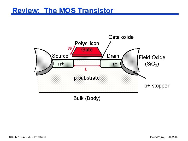
Review: The MOS Transistor Gate oxide Polysilicon W Gate Source n+ L Drain n+ Field-Oxide (Si. O 2) p substrate p+ stopper Bulk (Body) CSE 477 L 04 CMOS Inverter. 3 Irwin&Vijay, PSU, 2003

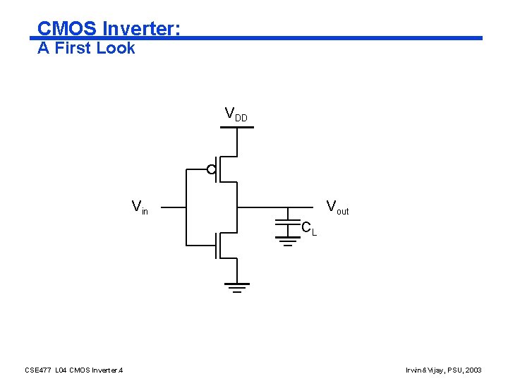
CMOS Inverter: A First Look VDD Vin Vout CL CSE 477 L 04 CMOS Inverter. 4 Irwin&Vijay, PSU, 2003

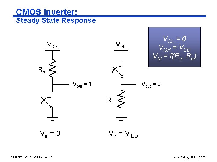
CMOS Inverter: Steady State Response VDD VOL = 0 VOH = VDD VM = f(Rn, Rp) Rp Vout = 1 Vout = 0 Rn Vin = 0 CSE 477 L 04 CMOS Inverter. 5 Vin = V DD Irwin&Vijay, PSU, 2003

CMOS Properties q Full rail-to-rail swing high noise margins l Logic levels not dependent upon the relative device sizes transistors can be minimum size ratioless q Always a path to Vdd or GND in steady state low output impedance (output resistance in k range) large fan-out (albeit with degraded performance) q Extremely high input resistance (gate of MOS transistor is near perfect insulator) nearly zero steady-state input current q No direct path steady-state between power and ground no static power dissipation q Propagation delay function of load capacitance and resistance of transistors CSE 477 L 04 CMOS Inverter. 6 Irwin&Vijay, PSU, 2003

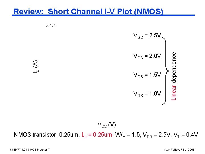
Review: Short Channel I-V Plot (NMOS) X 10 -4 ID (A) VGS = 2. 0 V VGS = 1. 5 V VGS = 1. 0 V Linear dependence VGS = 2. 5 V VDS (V) NMOS transistor, 0. 25 um, Ld = 0. 25 um, W/L = 1. 5, VDD = 2. 5 V, VT = 0. 4 V CSE 477 L 04 CMOS Inverter. 7 Irwin&Vijay, PSU, 2003

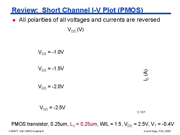
Review: Short Channel I-V Plot (PMOS) l All polarities of all voltages and currents are reversed VDS (V) VGS = -1. 5 V ID (A) VGS = -1. 0 V VGS = -2. 5 V X 10 -4 PMOS transistor, 0. 25 um, Ld = 0. 25 um, W/L = 1. 5, VDD = 2. 5 V, VT = -0. 4 V CSE 477 L 04 CMOS Inverter. 8 Irwin&Vijay, PSU, 2003

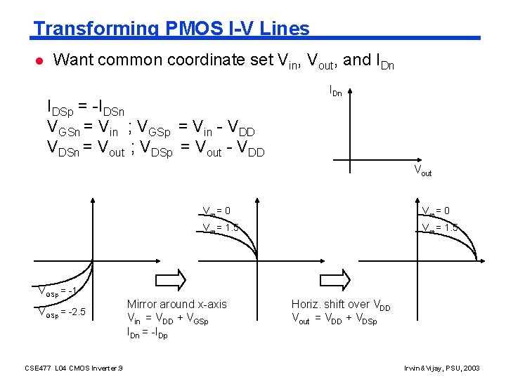
Transforming PMOS I-V Lines l Want common coordinate set Vin, Vout, and IDn IDSp = -IDSn VGSn = Vin ; VGSp = Vin - VDD VDSn = Vout ; VDSp = Vout - VDD IDn Vout Vin = 0 Vin = 1. 5 VGSp = -1 VGSp = -2. 5 CSE 477 L 04 CMOS Inverter. 9 Mirror around x-axis Vin = VDD + VGSp IDn = -IDp Horiz. shift over VDD Vout = VDD + VDSp Irwin&Vijay, PSU, 2003

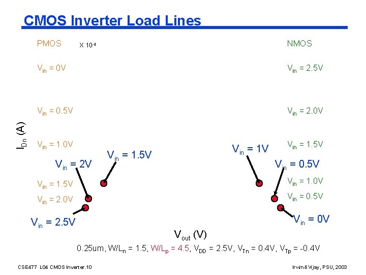
CMOS Inverter Load Lines IDn (A) PMOS NMOS X 10 -4 Vin = 0 V Vin = 2. 5 V Vin = 0. 5 V Vin = 2. 0 V Vin = 1. 0 V Vin = 2 V Vin = 1. 5 V Vin = 0. 5 V Vin = 1. 0 V Vin = 2. 0 V Vin = 0. 5 V Vin = 0 V Vin = 2. 5 V Vout (V) 0. 25 um, W/Ln = 1. 5, W/Lp = 4. 5, VDD = 2. 5 V, VTn = 0. 4 V, VTp = -0. 4 V CSE 477 L 04 CMOS Inverter. 10 Irwin&Vijay, PSU, 2003

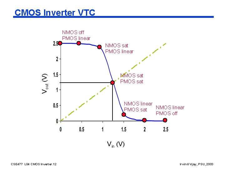
CMOS Inverter VTC NMOS off PMOS linear Vout (V) NMOS sat PMOS linear NMOS sat PMOS sat NMOS linear PMOS sat PMOS off Vin (V) CSE 477 L 04 CMOS Inverter. 12 Irwin&Vijay, PSU, 2003

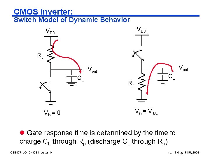
CMOS Inverter: Switch Model of Dynamic Behavior VDD Rp Vout CL Vin = 0 CL Rn Vin = V DD l Gate response time is determined by the time to charge CL through Rp (discharge CL through Rn) CSE 477 L 04 CMOS Inverter. 14 Irwin&Vijay, PSU, 2003

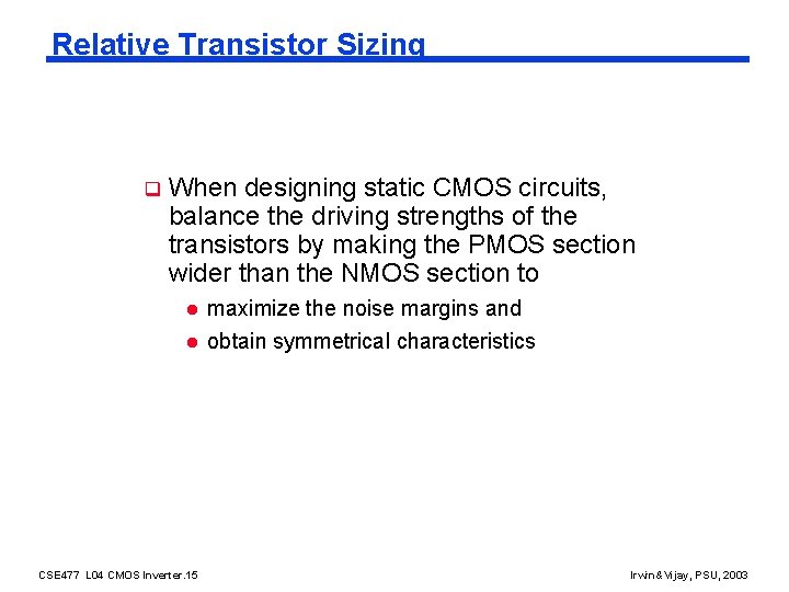
Relative Transistor Sizing q When designing static CMOS circuits, balance the driving strengths of the transistors by making the PMOS section wider than the NMOS section to l maximize the noise margins and l obtain symmetrical characteristics CSE 477 L 04 CMOS Inverter. 15 Irwin&Vijay, PSU, 2003

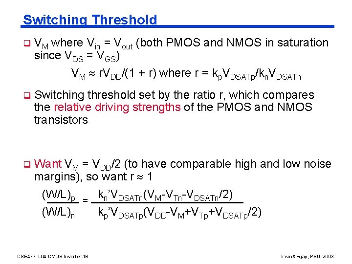
Switching Threshold q VM where Vin = Vout (both PMOS and NMOS in saturation since VDS = VGS) VM r. VDD/(1 + r) where r = kp. VDSATp/kn. VDSATn q Switching threshold set by the ratio r, which compares the relative driving strengths of the PMOS and NMOS transistors q Want VM = VDD/2 (to have comparable high and low noise margins), so want r 1 (W/L)p (W/L)n = CSE 477 L 04 CMOS Inverter. 16 kn’VDSATn(VM-VTn-VDSATn/2) kp’VDSATp(VDD-VM+VTp+VDSATp/2) Irwin&Vijay, PSU, 2003

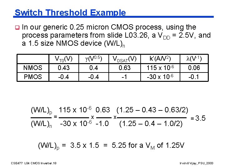
Switch Threshold Example q In our generic 0. 25 micron CMOS process, using the process parameters from slide L 03. 26, a VDD = 2. 5 V, and a 1. 5 size NMOS device (W/L)n NMOS PMOS VT 0(V) 0. 43 -0. 4 (V 0. 5) 0. 4 -0. 4 VDSAT(V) 0. 63 -1 (V-1) 0. 06 -0. 1 k’(A/V 2) 115 x 10 -6 -30 x 10 -6 (W/L)p 115 x 10 -6 0. 63 (1. 25 – 0. 43 – 0. 63/2) (W/L)n = -30 x x 10 -6 -1. 0 x (1. 25 – 0. 4 – 1. 0/2) = 3. 5 (W/L)p = 3. 5 x 1. 5 = 5. 25 for a VM of 1. 25 V CSE 477 L 04 CMOS Inverter. 18 Irwin&Vijay, PSU, 2003

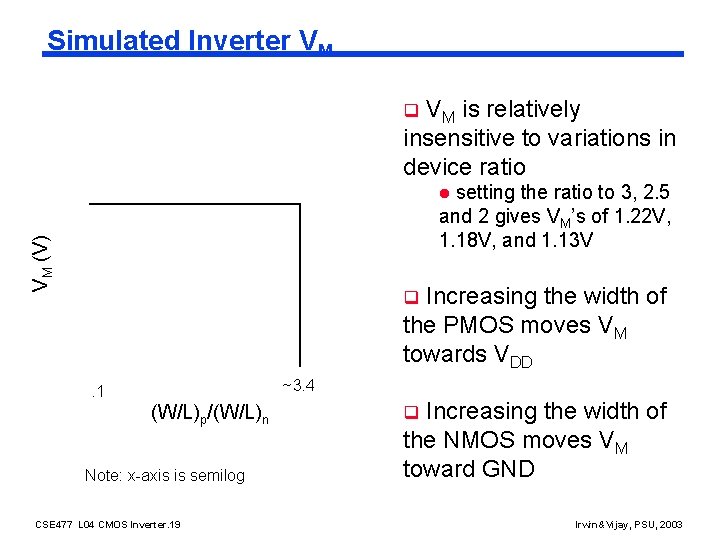
Simulated Inverter VM VM is relatively insensitive to variations in device ratio q setting the ratio to 3, 2. 5 and 2 gives VM’s of 1. 22 V, 1. 18 V, and 1. 13 V VM (V) l Increasing the width of the PMOS moves VM towards VDD q ~3. 4 . 1 (W/L)p/(W/L)n Note: x-axis is semilog CSE 477 L 04 CMOS Inverter. 19 Increasing the width of the NMOS moves VM toward GND q Irwin&Vijay, PSU, 2003

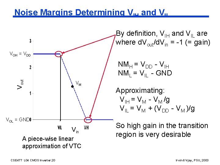
Noise Margins Determining VIH and VIL By definition, VIH and VIL are where d. Vout/d. Vin = -1 (= gain) VOH = VDD Vout NMH = VDD - VIH NML = VIL - GND VM VOL = GND Vin A piece-wise linear approximation of VTC CSE 477 L 04 CMOS Inverter. 20 Approximating: VIH = VM - VM /g VIL = VM + (VDD - VM )/g So high gain in the transition region is very desirable Irwin&Vijay, PSU, 2003

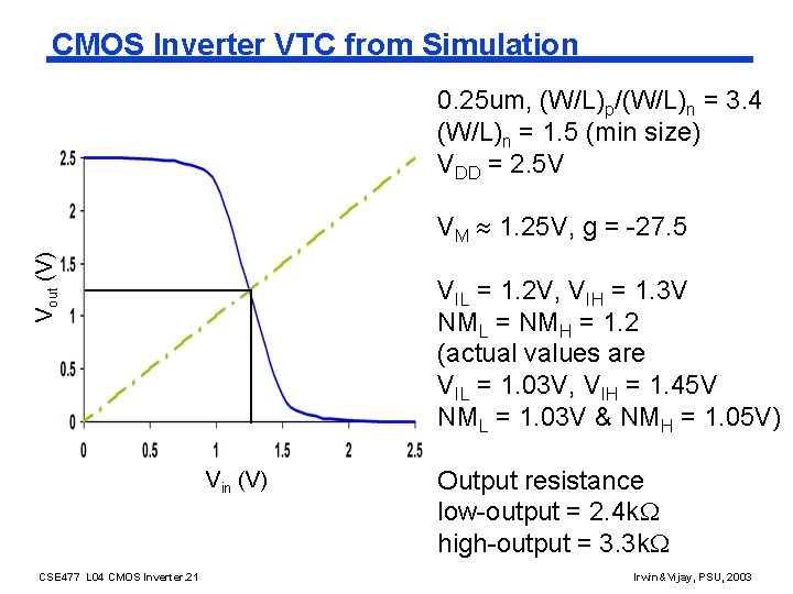
CMOS Inverter VTC from Simulation 0. 25 um, (W/L)p/(W/L)n = 3. 4 (W/L)n = 1. 5 (min size) VDD = 2. 5 V Vout (V) VM 1. 25 V, g = -27. 5 VIL = 1. 2 V, VIH = 1. 3 V NML = NMH = 1. 2 (actual values are VIL = 1. 03 V, VIH = 1. 45 V NML = 1. 03 V & NMH = 1. 05 V) Vin (V) CSE 477 L 04 CMOS Inverter. 21 Output resistance low-output = 2. 4 k high-output = 3. 3 k Irwin&Vijay, PSU, 2003

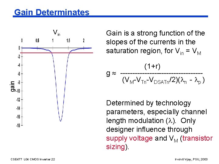
Gain Determinates gain Vin Gain is a strong function of the slopes of the currents in the saturation region, for Vin = VM (1+r) g -----------------(VM-VTn-VDSATn/2)( n - p ) Determined by technology parameters, especially channel length modulation ( ). Only designer influence through supply voltage and VM (transistor sizing). CSE 477 L 04 CMOS Inverter. 22 Irwin&Vijay, PSU, 2003

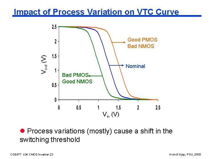
Impact of Process Variation on VTC Curve Vout (V) Good PMOS Bad NMOS Nominal Bad PMOS Good NMOS Vin (V) l Process variations (mostly) cause a shift in the switching threshold CSE 477 L 04 CMOS Inverter. 23 Irwin&Vijay, PSU, 2003

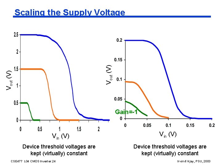
Vout (V) Scaling the Supply Voltage Gain=-1 Vin (V) Device threshold voltages are kept (virtually) constant CSE 477 L 04 CMOS Inverter. 24 Vin (V) Device threshold voltages are kept (virtually) constant Irwin&Vijay, PSU, 2003

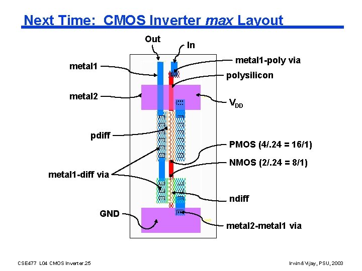
Next Time: CMOS Inverter max Layout Out In metal 1 -poly via metal 1 polysilicon metal 2 VDD pdiff PMOS (4/. 24 = 16/1) NMOS (2/. 24 = 8/1) metal 1 -diff via ndiff GND metal 2 -metal 1 via CSE 477 L 04 CMOS Inverter. 25 Irwin&Vijay, PSU, 2003

Next Lecture and Reminders q Next lecture l IC manufacturing - Reading assignment – Rabaey, et al, 2. 1 -2. 3 presented by guest lecturer Greg Link q Reminders l HW 2 due September 30 l Project team and title due September 18 th (next class!) Evening midterm exam scheduled l - Monday, October 20 th , 20: 15 to 22: 15, Location TBD - Please let me know ASAP (via email) if you have a conflict CSE 477 L 04 CMOS Inverter. 26 Irwin&Vijay, PSU, 2003