An extensive course on ELECTRO STATIC DISCHARGE AWARENESS


 are the most severe form of Electromagnet Interference (EMI).")


")


")


 { The basic human body model consists of body capacitance")
")


")


- Slides: 92
An extensive course on ELECTRO STATIC DISCHARGE AWARENESS AND CONTROL
Examples : Lightning Zapping
An atom is made up of charges An atom is made up of charges. In its stable state, the size of the positive charge at the centre (nucleus) of an atom is balanced by the size of all the negative charges of the electrons, making it neutral overall. The electrons whirl around the centre like planets.
Creating a charge imbalance Electron “lost” When an atom loses an electron, it has a charge imbalance. Since this atom has lost an electron, which is a negative charge, the atom is now a positive charge. When it gains an extra electron, an atom becomes a negative charge.
A discharge This powerful, rapid movement of charges can damage electronic components. Let’s see it again! When something which has a charge imbalance is brought close to or touches something else, a stream of charges might move, to try to bring the atoms back to their stable balanced condition. This movement of charges is called a discharge.
WHAT IS ESD? ELECTRO STATIC DISCHARGE IS DEFINED AS THE TRANSFER OF ELECTRO STATIC CHARGES BETWEEN BODIES AT DIFFERENT POTENTIAL CAUSED BY DIRECT CONTACT OR INDUCED ELECTRO STATIC FIELD. ESD EVENT IT IS AN UNPLANNED OCCURANCE OF ELECTRO- STATIC DISCHARGE
What is ESD—Electrostatic Discharges (ESD) are the most severe form of Electromagnet Interference (EMI). The human body can build up static charges that range up to 25, 000 volts. These build -ups can discharge very rapidly into a electrically grounded body, or device. Placing a 25, 000 -volt surge through any electronic device is potentially damaging to it.
The most common causes of ESD are: Moving people Improper grounding Unshielded cables Poor connections Moving machines Low humidity (hot and dry conditions)
Figure 13 -14: Power Transmission System
Figure 13 -15: Grounds on IC Chips
To avoid damaging static-sensitive devices, the following procedures will help to minimize the chances of destructive static discharges: Some devices used to remove solder from circuit boards and chips can cause high static discharges that may damage the good devices on the board. The device in question is referred to as a solder-sucker, and is available in antistatic versions for use with MOS devices.
Triboelectric generation Basic Principles (2)
When materials are in contact When two materials are in intimate contact, they share electrons which are at their surfaces.
The triboelectric charge of two materials in contact.
When materials are in contact It is possible for electrons to be “stolen” from one When two materials are in intimate contact, they share material by nuclei in the other material, because they electrons which are at their surfaces. have a stronger force
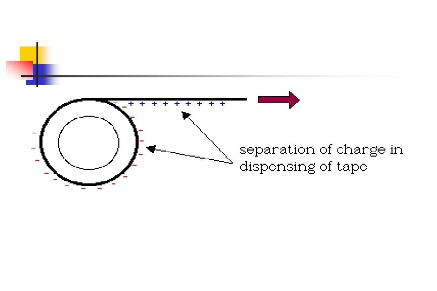
When the materials are separated Electrons “lost” Electrons “gained” When these materials are separated, electrons are removed from one material and are transferred to the other material.
When the materials are separated Electrons “lost” Electrons “gained” This action takes place with types of materials. With When these materials areall separated, electrons are insulators, the charges remain thetransferred points of contact. removed from one material andatare to the A charge spreads all overmaterial. an ungrounded conductor. other
The triboelectric charge when two materials placed in contact are then separated.
When the materials are separated Electrons “lost” Electrons “gained” This action takes place with all types of materials. With insulators, the charges remain at the points of contact. A charge spreads all over an ungrounded conductor. The loss and gain of these electrons creates an imbalance of negative and positive charges on the surface of each material.
When the materials are separated Electrons “lost” Electrons “gained” When the surfaces are rough, this intimacy and separation is assisted by rubbing the materials together.
When the materials are separated Electrons “lost” Electrons “gained” The size of the charge (imbalance) depends on the intimacy of the contact, how fast they were separated, the humidity and the kinds of materials
When the materials are separated Electrons “lost” Electrons “gained” The drier the air (lower relative humidity, RH) the higher the generated charge
The creation of a charge when materials are separated is termed “triboelectric charging”
Charging by Induction Basic Principles
Charging by induction The charge imbalance on a surface produces an electric field. The presence of this very strong force causes similar charges on the surfaces of nearby
Charging by induction If the conductor is grounded while it is still influenced by the electric field, these repelled charges go to earth, thus maintaining a charge balance in the areas of the conductor that are not affected by the electric field.
Charging by induction
Walking on carpet Thoughts and theories
Walking across carpet Walking across a carpet creates a charge imbalance on the lower surface of shoes.
A strong electric field This charge imbalance creates a strong electric field that emanates in all directions. The material in the sole of shoe enables a strong field to influence charges within foot.
An induced charge Since the body is relatively conductive, the charges that are repelled from the lower regions of my foot set up a charge throughout the rest of my body. But the body still has a balanced charge overall (it has not lost or gained any charges).
Contacting a source of While you are still charges on the carpet (still influenced by the electric field on the sole of your shoe), you briefly touch a metallic object (a chair, table, door knob, metal stapler, etc. ) This enables charges to be provided by the metallic object.
Charging through the air If the charge imbalance on my body is large enough, I do not need to touch the object, as the imbalance could allow a movement of charges through the air. This movement of charges is thus producing an overall charge imbalance in my body, since I was previously neutral overall.
An overall charge imbalance Therefore, after that brief encounter with the metallic object, my body now has an overall charge imbalance.
Removing that charge The only way to remove the possibility of damaging an ESD-sensitive device or assembly is to remove the overall charge imbalance on my body. This is done by connecting my body to the ready source of charges that is at the same reference potential as the item I wish to handle - using a wrist strap or foot strap.
ELECTROSTATIC DISCHARGE PROCESS 1. Charge is generated on the surface of an insulator. 2. This charge is transfered to a conductor by contact or induction. 3. The charged conductor comes near a metal object (grounded or ungrounded) and a discharge occurs. 4. When a discharge occurs to an ungrounded object, the discharge current flows through the capacitance between the object and ground.
STATIC GENERATION THE STATIC CHARGE IS GENERATED BY IMBALANCE IN THE MOLECULAR CAUSING STRIPPING STRUCTURE OF BY RUBBING; NEGATIVELYCHARGED ELECTRONS WITH ONE MATERIAL GETTING PASITIVE CHARGE AND OTHER NEGATIVE CAUSE FOR STATIC CHARGE ð FRICTION ð SEPERATION ð INDUCTION
CAUSES FOR ESD GENERATION F WALKING ON SYNTHETIC SURFACE ESD F RELATIVE MOVEMENT ON CHAIR F TABLE, COMPUTER, PLASTIC PARTS NYLON OR SYNTHETIC CLOTHES F CLEANING WITH COMPRESSED AIR F CLEANING WITH SOLVENT
FACTORS: ø TYPE OF MATERIAL ø RELATIVE HUMIDITY ø TYPE OF CLOTHING ø SPEED AND MANNER OF WALKING ø BODY RESISTANCE
RECORDED ESD ACCIDENTS L In 1937, The German flying boat Hinderburg arriving in Lakehurst, New Jersey, caught fire while anchoring at its landing mast. L In 1970’s, in USA, a space craft launching rocket exploded during the fueling operation, killing 3 engineers. L In January, 1985, during the assembly of a missile in Germany, the motor case made of Kelvar, got rubbbed against the cushioning in its container. The ESD generated caused the highly flammable propellant to catch fire and the motor exploded, killing 3 people. L 3 to 30% of Integrated Circuits manufactured every year die in “infancy” due to ESD.
Device sensitivity to Electrostatic Discharge At higher magnificat ion the pit in the area between the base and emitter becomes more obvious
Device sensitivity to Electrostatic Discharge At this magnific ation see the 1/2 of the width of the material has been destroyed.
Statistics 40 – 50% EQUIPMENTS HAVE FAILED IN THE FIELD DUE TO ESD
SENSITIVE CONSTITUENTS FAILURE MODES MOS STRUCTURES SHORT BIPOLAR JUNCTIONS LEAKAGE FILM RESISTORS VALUE SHIFT METALIZATION STRIPES OPEN FIELD PERFECT STRUCTURES OPERATIONAL PIEZOELECTRIC CRYSTALS DEGRADED CLOSELY SPACED CONDUCTORS DEGRADED
ESD SOURCES MAN MADE: • PLASTICS • CONDUCTORS • FURNITURES • VINYL FLOOR • COOLING FANS WITH PLASTIC BLADES • PRINTERS/COPIERS • PAPER • NYLON & WOOLLEN GARMENTS • COMPRESSED AIR GUN
NATURAL: • HUMAN BODY • MOVEMENT OF CLOUDS
TYPICAL CHARGE GENERATORS PACKING HANDLING MATERIALS: âCOMMON POLYTHENE BAGS, WRAPS, ENVELOPES âCOMMON BUBBLE PACK FOAM âCOMMON PLASTIC TRAYS, PLASTIC TOTE BOXES, VIALS ASSEMBLY, CLEANING, TEST & REPAIR AREA ITEMS: âSPRAY CLEANERS âCOMMON SOLDER SUCKERS âCOMMON SOLDER IRONS âSOLVENT BRUSHING ( SYNTHETIC BRISTLES) âCLEANING, DRYING âTEPARATURE CHAMBERS
ESD VOLTAGE MEASUREMENT ELECTROSTATIC VOLTAGE MEANS OF STATIC GENERATION 10% RW 40% RW 55% RW PERSON WALKING ACROSS CARPET 35000 15000 7500 PERSON WALKING ACROSS VINYL FLOOR 12000 5000 3000 WORKER AT A BENCH 6000 800 400 CERAMIC DIPS IN PLASTIC TUBE 2000 700 400 CERAMIC DIPS IN VINYL SET UP TRAYS 11500 4000 2000 CIRCUIT AS BUBBLE PLASTIC COVER REMOVED 25000 20000 7000 CIRCUIT AS PACKED IN FOAM LINED SHIPPING BOX 21000 11000 5500
REASONS FOR DISBELIEF ESD DAMAGE : WHEN UNNOTICED? HUMAN SENSE OF FEELING OF STATIC AT 4000 V MUCH MORE HIGHER THAN SENSITIVITY OF COMPONENTS ; HARDLY ANY PHYSICAL DAMAGE ; ESD FAILURES CONSIDERED AS GENERAL COMPONENT FAILURE ; FAILURE MAY NOT BE INSTANT. (LATENT FAILURE)
GUIDE TO STATIC CONTROL MATERIALS SURFACE RESISTIVITY-OHMS PER SQUARE INSULATOR 1012 To 10 15 MATERIALS IN THIS RANGE ARE NOT EFFECTIVE FOR STATIC CONTROL
GUIDE TO STATIC CONTROL MATERIALS SURFACE RESISTIVITY-OHMS PER SQUARE ANTISTATIC 1010 To 10 12 THESE MATERIALS DO NOT GENERATE AND SUPPORT HIGH STATIC CHARGES. BUT DISCHARGE RATES ARE TOO SLOW FOR MOST INDUSTRIAL APPLICATIONS.
GUIDE TO STATIC CONTROL MATERIALS SURFACE RESISTIVITY-OHMS PER SQUARE STATIC DISSIPATORS ( PARTIALLY CONDUCTIVE) 106 To 10 9 MATERIALS MOST SUITABLE FOR STATIC CONTROL WORK SURFACES, FLOORING AND FLOOR MATS, SEALING, OVERALLS
GUIDE TO STATIC CONTROL MATERIALS SURFACE RESISTIVITY-OHMS PER SQUARE CONDUCTIVE 101 To MATERIALS FOR CONTAINERS AND HANDLING EQUIPMENT. BELOW 104 OHMS PER SQUARE EFFECTIVE STATIC SHIELDING IS POSSIBLE, OPERATOR SAFELY WILL BE 4 10 COMPROMISED IF THE EARTH PATH THROUGH BENCH MATS, FLOOR MATS AND FLOORING LESS THAN 5 X 10⁴ OHMS AND MAINS POWERED EQUIPMENT’S IN USE.
OBJECTIVES OF ESD CONTROL | PREVENTING STATIC CHARGE GENERATION |DISSIPATING THE DEVELOPED CHARGE |NEUTRALISING DEVELOPED CHARGE FOR A CHARGE FREE ZONE CONTROLLING OF ESD «WORK SURFACE «AIR «HUMAN BODY «FLOOR
DO’S þ MINIMISE HANDLING. þ KEEP PARTS IN ORIGINAL PACKING UNTILL READY FOR USE. þ USE ESD PROTECTIVE CONTAINERS AND BAGS. þ DISCHARGE STATIC BEFORE HANDLING DEVICE BY TOUCHING NEARBY GROUNDED SURFACE. þ HANDLE DEVICES BY THE BODY. þ TOUCH THE ESD PROTECTIVE PACKAGE BEFORE TOUCHING INSIDE OF DEVICE. þ KEEP A DUST FREE WORK AREA.
DONT’S ý TOUCH THE LEADS OF DEVICE. ý SLIDE ES DEVICES OVER ANY SURFACE. ý PUT MASKING TAPE ON PROGRAMMABLE IC’S. ý STORE OR CARRY SENSITIVE COMPONENTS OR ASSEMBLIES IN PLASTIC BAGS. ý STORE SENSITIVE THERMOCOLE/PLASTIC FOAM. COMPONENTS IN ý HANDLE ES DEVICES IN “NON ESD CONTROLLED” ENVIRONMENT.
ESD MODELS HAVE BEEN DEFINED TO DESCRIBE THE EFFECTS ON ESD SENSITIVE DEVICES: ÿ HUMAN BODY MODEL ÿ CHARGED DEVICE MODEL ÿ MACHINE MODEL
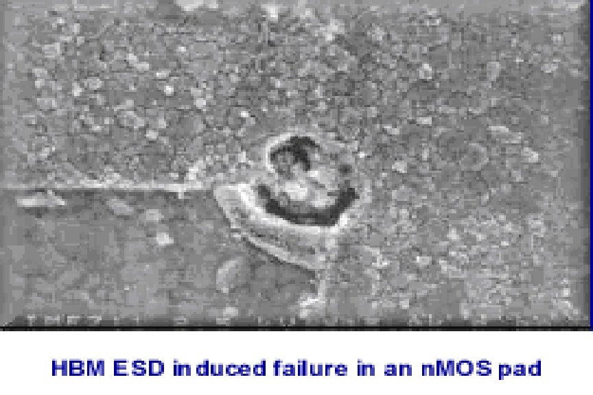
Human Body Model (HBM) { The basic human body model consists of body capacitance and resistance. The charge is stored in the body capacitance and the discharge occurs through the body resistance. { When a charged person handles or comes in close proximity to an ESD sensitive part, the part may be damaged by direct discharge or by an electro static field. Vb Cb Rb ^ <0. 1 m. H Cb : 50 to 350 p. F Rb : 150 to 10 KOhms Vb : 3 to 20 KV
Human Body Model (HBM)
HUMAN BODY CAPACITANCE AND RESISTANCE Rb ^ oo ^ 50 -100 p. F 50 p. F 100 p. F
TYPICAL ESD CURRENT WAVE FORM I ^ ^ 40 A. . . . tr=1 n. Sec tf=100 n. Sec t
Machine Model A discharge similar to the HBM event also can occur from a charged conductive object, such as a metallic tool or fixture. .
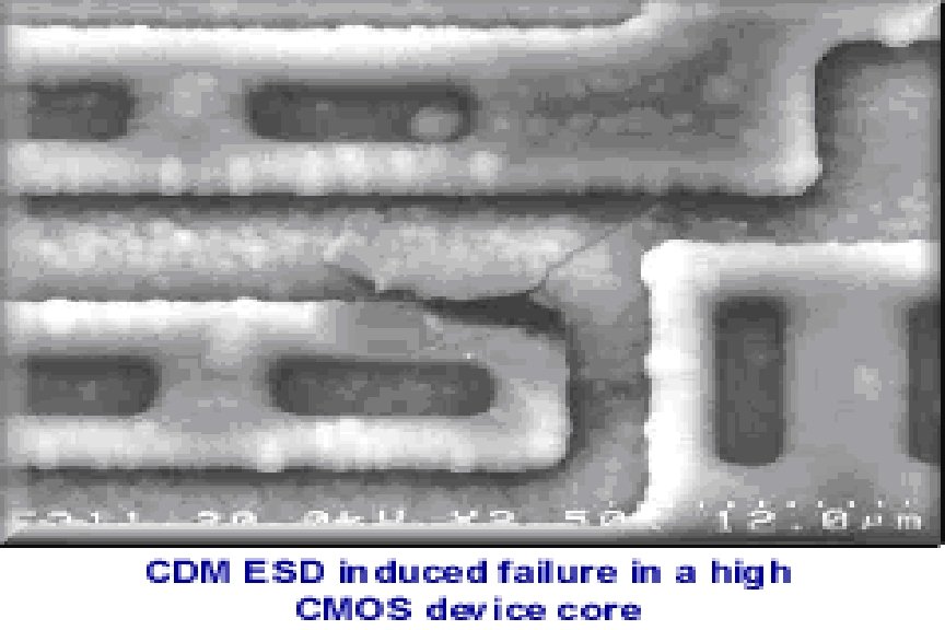
Charged Device Model The transfer of charge from an ESDS device is also an ESD event. A device may become charged, for example, from sliding down the feeder in an automated assembler. If it then contacts the insertion head or another conductive surface, a rapid discharge may occur from the device to the metal object. This event is known as the Charged Device Model (CDM).
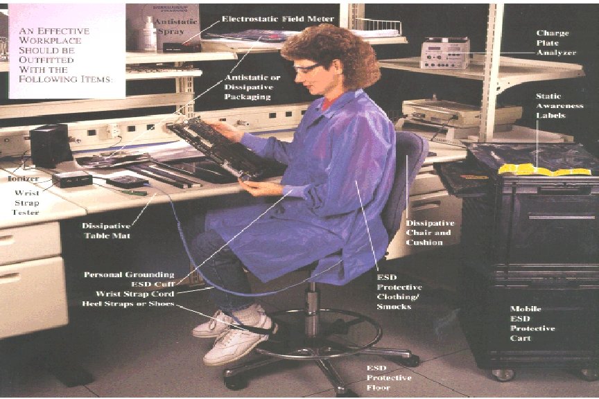
ESD CONTROL DEVICES F ANTISTATIC VINYL TABLE MAT F CONDUCTIVE FLOOR MAT F ESD LAMINATE F ESD WRIST STRAP F ESD HEEL STRAP F ESD TOE STRAP F COMMON POINT GROUND F ANTISTATIC BINS/TRAYS F PCB STORAGE RACK F CONDUCTIVE FOAM
ESD AUDIT
MATERIALS CLASSIFICATION MATERIAL CLASS SURFACE VOLUME RESISTIVITY SHIELDING 104 OR LESS 102 OR LESS CONDUCTIVE 105 OR LESS 104 OR LESS DISSIPATIVE 105 TO 1010 104 TO 109 ANTISTATIC 1010 TO 1012 INSULATIVE >1015 -->1014
ESD AUDIT Ã PERSONNEL TRAINING FOR ESD PREVENTIVE Ã AWARENESS TRAINING Ã CERTIFICATION TRAINING Ã CONTROL PROGRAM AUDIT
ESD TEST & MEASURING INSTRUMENTS F STATIC CHARGE METER FWRIST STRAP AND GROUND TESTER FFOOTWEAR TESTER FSURFACE RESISTIVITY METER FSTATIC SENSOR FCONTINUOUS WRIST STRAP MONITOR FCONTINUOUS WORK STATION MONITOR FTEMPARATURE AND HUMIDITY INDICATOR
TESTING EVALUATION The test evaluation report consists of the following test areas for each ESD item/s: v. POINT TO POINT SURFACE RESISTIVITY TOP/BOTTOM v. POINT TO POINT SURFACE RESISTIVITY IN/OUT v. SURFACE TO GROUND RESISTANCE v. PERSON TO GROUND RESISTANCE v. STATIC CHARGE MEASURING TEST v. STATIC SHIELDING TEST
TESTING EVALUATION The tests are generally conducted for W the following item/s: W Antistatic P. E Bags WESD Mat W Static Shield Bags conductive Mat W Conductive Bags W Work Surface W Conductive Grid Bags W ESD Laminate W Antistatic Aprons W Wrist Strap W Conductive Brush W Heel Strap W Foot Wear W ESD Chair
PERSONAL GROUNDING Two types of Personal Grounding: Wrist Straps Footwear
WRIST STRAPS ð Daily Check with Wrist Strap Worn ð Test with a Wrist Strap tester
Floor ð Point to Point
Floor ð Resistance to Ground
Garments ð Point to Point
Garments ð Point to Ground ð May need person wearing garment Needs to be connected to ground as wor n
Chair ð Check all parts of Chairs to Ground ð Seat, Backrest, Armrest, Foot Rest
TYPES OF ESD DAMAGE CATASTROPHIC FAILURE ßUPSET FAILURE
SHIELDING FARADAY CAGE Types of Faraday Cages • Metallized & Conductive Shielding Bags • Conductive tote box with cover
A hollow conductor Michael Faraday A Faraday Cage is a hollow conductor.
WORK STATION
Electrostatic Voltmeter (ESV)
Measurement of Static Electricity Static electricity is measured in coulombs. The charge "q" on an object is determined by the product of the capacitance of the object "C" and the voltage potential on the object (V): q=CV Commonly, however, we speak of the electrostatic potential on an object, which is expressed as voltage.
ESD Damage-How Devices Fail Electrostatic damage to electronic devices can occur at any point from manufacture to field service. Damage results from handling the devices in uncontrolled surroundings or when poor ESD control practices are used. Generally damage is classified as either a catastrophic failure or a latent defect.