Lecture 4 The CMOS Inverter Dynamic properties Week




- Slides: 58

Lecture 4 The CMOS Inverter Dynamic properties

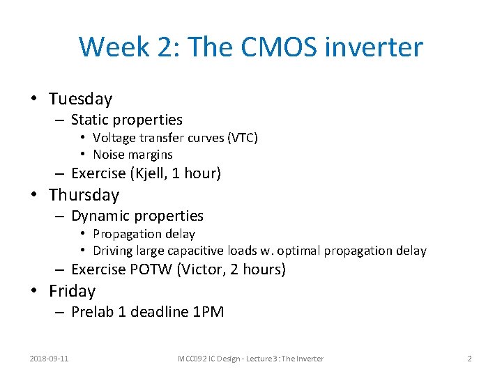
Week 2: The CMOS inverter • Tuesday – Static properties • Voltage transfer curves (VTC) • Noise margins – Exercise (Kjell, 1 hour) • Thursday – Dynamic properties • Propagation delay • Driving large capacitive loads w. optimal propagation delay – Exercise POTW (Victor, 2 hours) • Friday – Prelab 1 deadline 1 PM 2018 -09 -11 MCC 092 IC Design - Lecture 3: The Inverter 2

Last time? Muddy? • How switching voltage is calculated • NOR/NAND gate VTC • Noise margins – How calculate them – Are they accurate from simplified models? – Where does 1/8 come from in noise margin example? – Butterfly diagram • Cox what is that? 2018 -09 -13 Lecture 4: CMOS Inverter dynamics 3

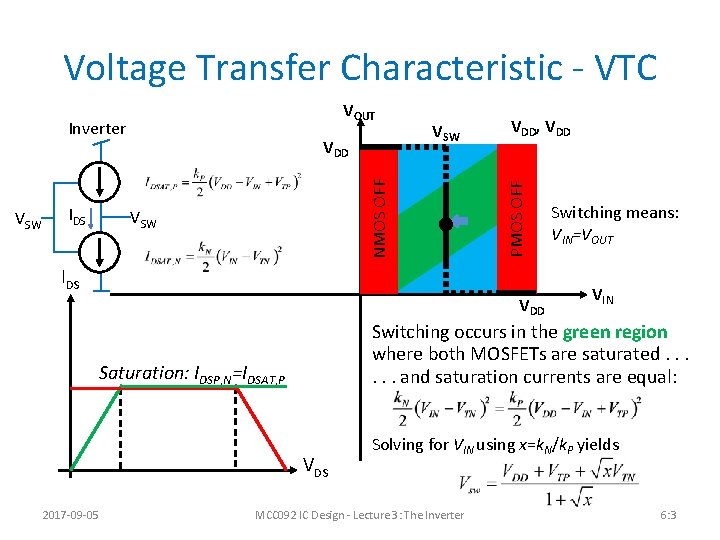
Voltage Transfer Characteristic - VTC Inverter IDS NMOS OFF VSW VDD, VDD PMOS OFF VOUT IDS VDD VIN Switching occurs in the green region where both MOSFETs are saturated. . . and saturation currents are equal: Saturation: IDSP, N=IDSAT, P VDS 2017 -09 -05 Switching means: VIN=VOUT Solving for VIN using x=k. N/k. P yields MCC 092 IC Design - Lecture 3: The Inverter 6: 3

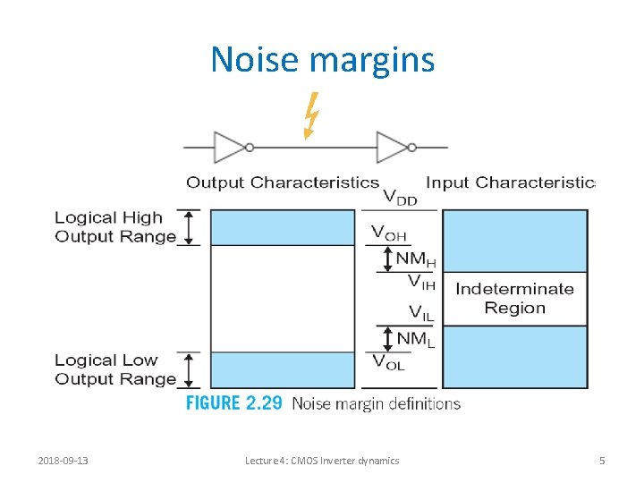
Noise margins 2018 -09 -13 Lecture 4: CMOS Inverter dynamics 5

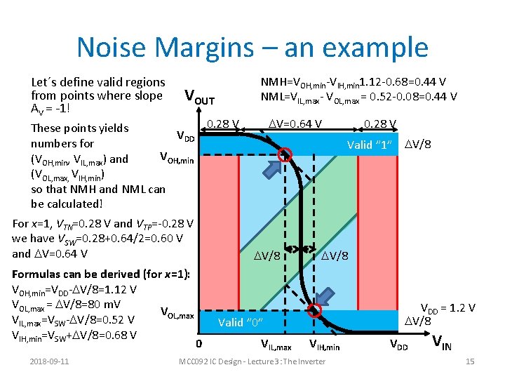
Noise Margins – an example Let´s define valid regions from points where slope AV = -1! NMH=VOH, min-VIH, min 1. 12 -0. 68=0. 44 V NML=VIL, max- VOL, max = 0. 52 -0. 08=0. 44 V VOUT DV=0. 64 V 0. 28 V These points yields VDD numbers for VOH, min (VOH, min, VIL, max) and (VOL, max, VIH, min) so that NMH and NML can be calculated! For x=1, VTN=0. 28 V and VTP=-0. 28 V we have VSW=0. 28+0. 64/2=0. 60 V and DV=0. 64 V Formulas can be be derived (forx=1): VOH, min=VDD-DV/8=1. 12 -DV/8 V VOL, max = DV/8=80 DV/8 m. V VOL, max VIL, max=VSW-DV/8=0. 52 -DV/8 V 0 VIH, min=VSW+DV/8=0. 68 +DV/8 V 2018 -09 -11 Valid ” 1” DV/8 VDD = 1. 2 V DV/8 Valid ” 0” 0 0. 28 V VIL, max VIH, min MCC 092 IC Design - Lecture 3: The Inverter VDD VIN 15

Quick question • Have you tried solving prelab 3 yet? 2018 -09 -11 MCC 092 IC Design - Lecture 3: The Inverter 7

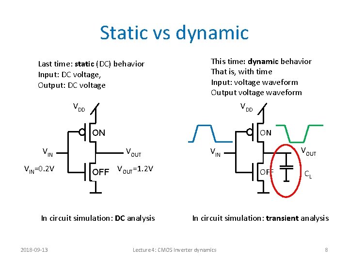
Static vs dynamic Last time: static (DC) behavior Input: DC voltage, Output: DC voltage This time: dynamic behavior That is, with time Input: voltage waveform Output voltage waveform VDD ON ON VIN=0. 2 V VOUT OFF VOUT=1. 2 V In circuit simulation: DC analysis 2018 -09 -13 VOUT VIN OFF CL In circuit simulation: transient analysis Lecture 4: CMOS Inverter dynamics 8

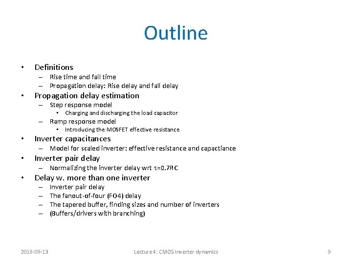
Outline • Definitions – Rise time and fall time – Propagation delay: Rise delay and fall delay • Propagation delay estimation – Step response model • Charging and discharging the load capacitor – Ramp response model • Introducing the MOSFET effective resistance • Inverter capacitances – Model for scaled inverter: effective resistance and capactiance • Inverter pair delay • Delay w. more than one inverter – Normalizing the inverter delay wrt t=0. 7 RC – – 2018 -09 -13 Inverter pair delay The fanout-of-four (FO 4) delay The tapered buffer, finding sizes and number of inverters (Buffers/drivers with branching) Lecture 4: CMOS Inverter dynamics 9

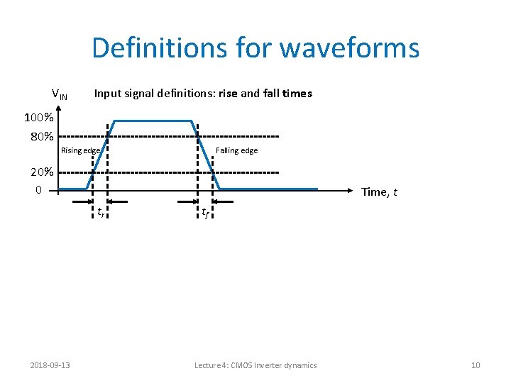
Definitions for waveforms VIN Input signal definitions: rise and fall times 100% 80% Rising edge Falling edge 20% 0 Time, t tr 2018 -09 -13 tf Lecture 4: CMOS Inverter dynamics 10

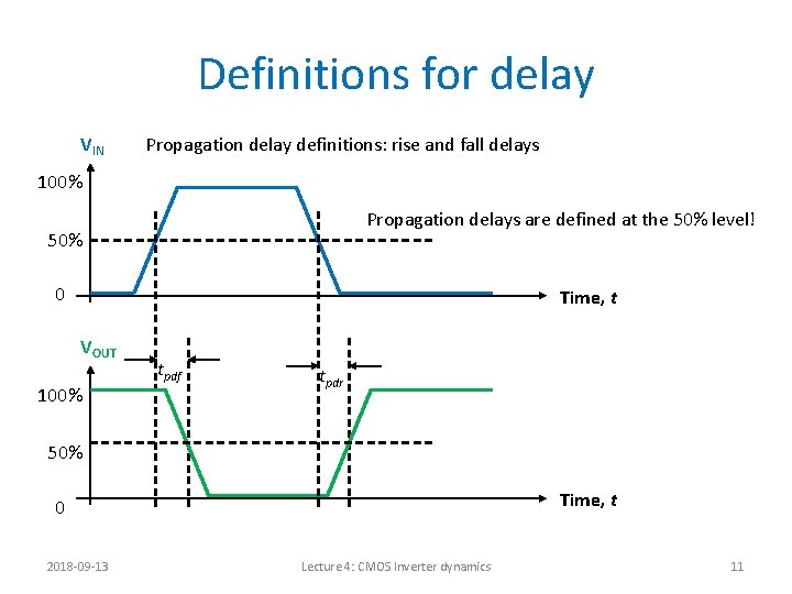
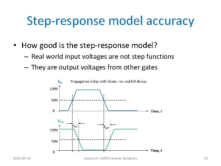
Definitions for delay VIN Propagation delay definitions: rise and fall delays 100% Propagation delays are defined at the 50% level! 50% 0 Time, t VOUT 100% tpdf tpdr 50% Time, t 0 2018 -09 -13 Lecture 4: CMOS Inverter dynamics 11

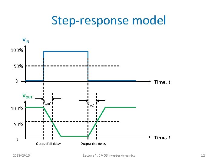
Step-response model VIN 100% 50% 0 Time, t VOUT 100% tpdf tpdr 50% 0 2018 -09 -13 Time, t Output fall delay Output rise delay Lecture 4: CMOS Inverter dynamics 12

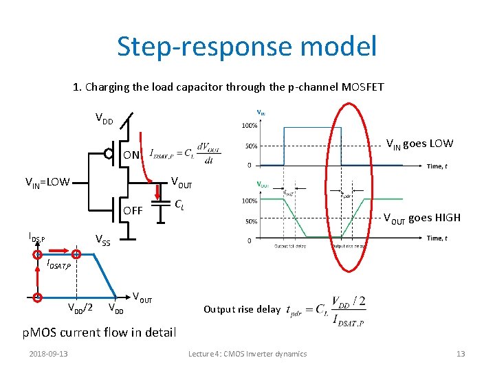
Step-response model 1. Charging the load capacitor through the p-channel MOSFET VDD VIN goes LOW ON VIN=LOW VOUT OFF IDS, P CL VOUT goes HIGH VSS IDSAT, P VDD/2 VDD VOUT Output rise delay p. MOS current flow in detail 2018 -09 -13 Lecture 4: CMOS Inverter dynamics 13

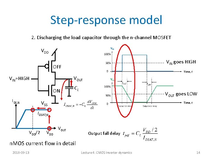
Step-response model 2. Discharging the load capacitor through the n-channel MOSFET VDD VIN goes HIGH OFF VIN=HIGH VOUT ON IDS, N CL VOUT goes LOW VSS IDSAT, N VDD/2 VDD VOUT Output fall delay n. MOS current flow in detail 2018 -09 -13 Lecture 4: CMOS Inverter dynamics 14

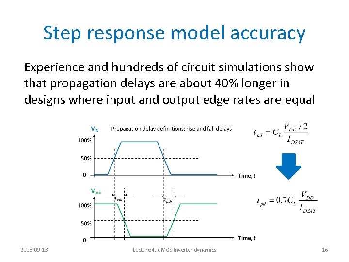
Step-response model accuracy • How good is the step-response model? – Real world input voltages are not step functions – They are output voltages from other gates 2018 -09 -13 Lecture 4: CMOS Inverter dynamics 15

Step response model accuracy Experience and hundreds of circuit simulations show that propagation delays are about 40% longer in designs where input and output edge rates are equal 2018 -09 -13 Lecture 4: CMOS Inverter dynamics 16

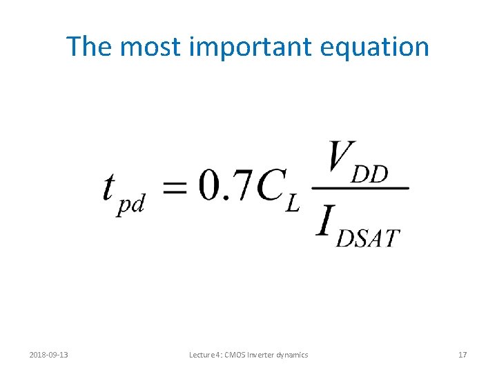
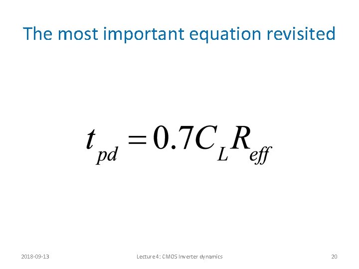
The most important equation 2018 -09 -13 Lecture 4: CMOS Inverter dynamics 17

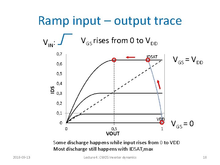
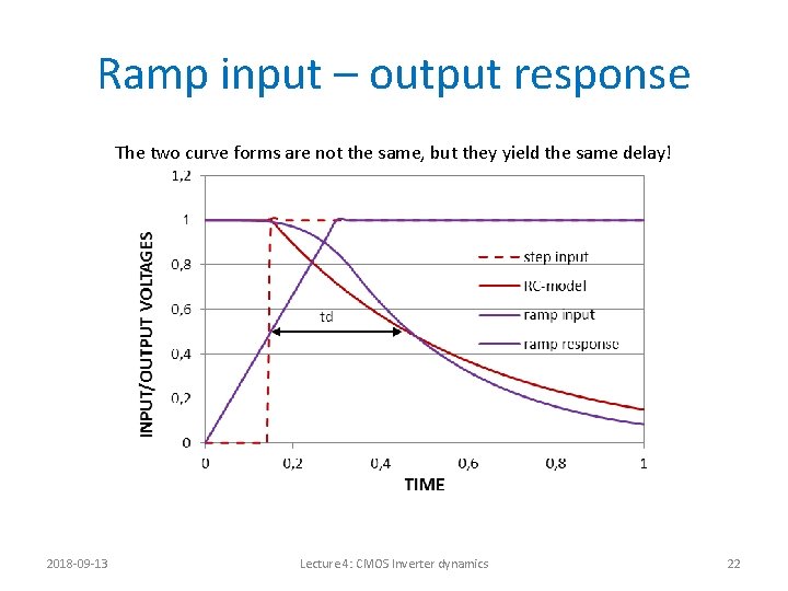
Ramp input – output trace VIN: VGS rises from 0 to VDD VGS = 0 Some discharge happens while input rises from 0 to VDD Most discharge still happens with IDSAT, max 2018 -09 -13 Lecture 4: CMOS Inverter dynamics 18

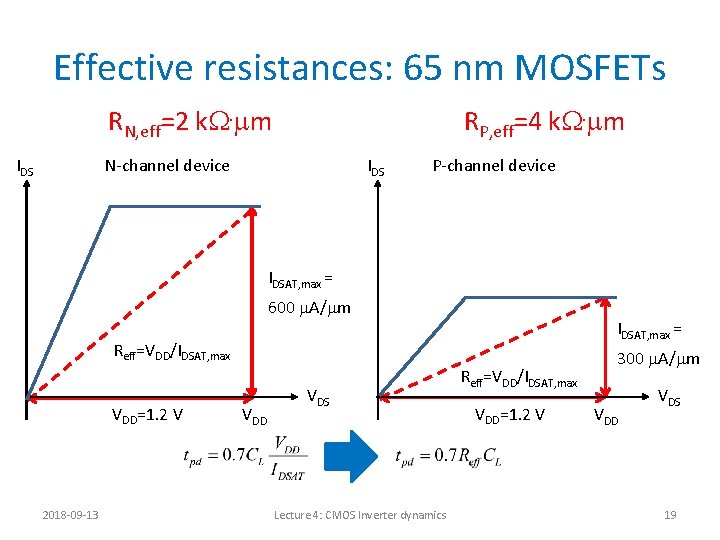
Effective resistances: 65 nm MOSFETs RN, eff=2 k. W. mm IDS RP, eff=4 k. W. mm IDS N-channel device P-channel device IDSAT, max = 600 m. A/mm IDSAT, max = Reff=VDD/IDSAT, max VDD=1. 2 V 2018 -09 -13 VDD VDS Lecture 4: CMOS Inverter dynamics Reff=VDD/IDSAT, max VDD=1. 2 V 300 m. A/mm VDD VDS 19

The most important equation revisited 2018 -09 -13 Lecture 4: CMOS Inverter dynamics 20

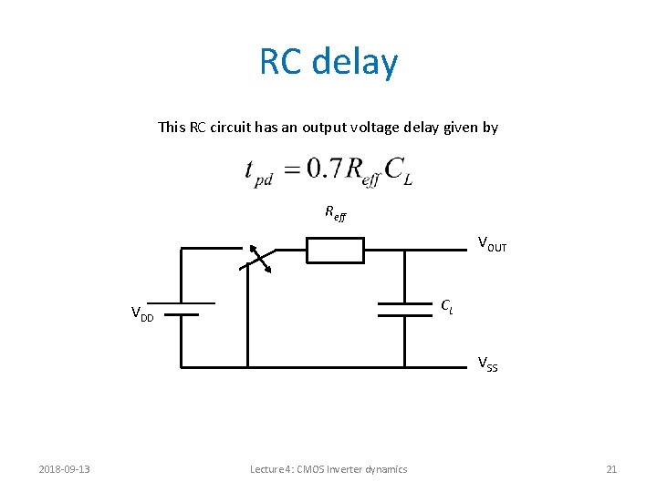
RC delay This RC circuit has an output voltage delay given by Reff VOUT CL VDD VSS 2018 -09 -13 Lecture 4: CMOS Inverter dynamics 21

Ramp input – output response The two curve forms are not the same, but they yield the same delay! 2018 -09 -13 Lecture 4: CMOS Inverter dynamics 22

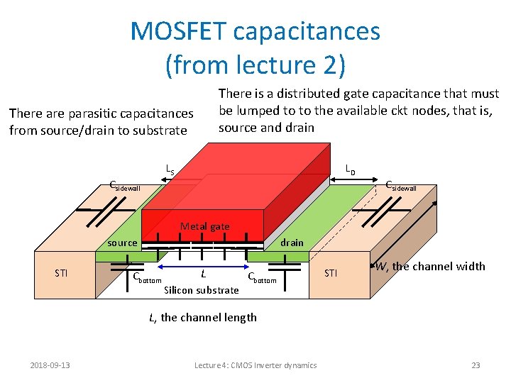
MOSFET capacitances (from lecture 2) There is a distributed gate capacitance that must be lumped to to the available ckt nodes, that is, source and drain There are parasitic capacitances from source/drain to substrate LD LS Csidewall Metal gate source STI drain Cbottom L Silicon substrate Cbottom STI W, the channel width L, the channel length 2018 -09 -13 Lecture 4: CMOS Inverter dynamics 23

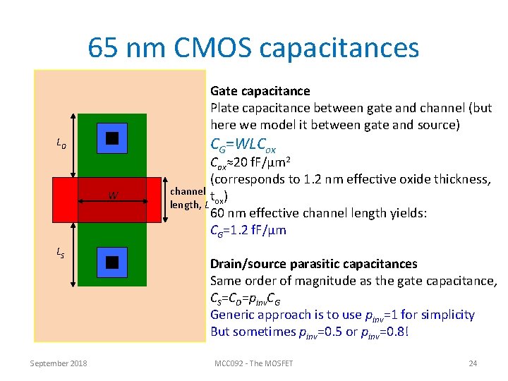
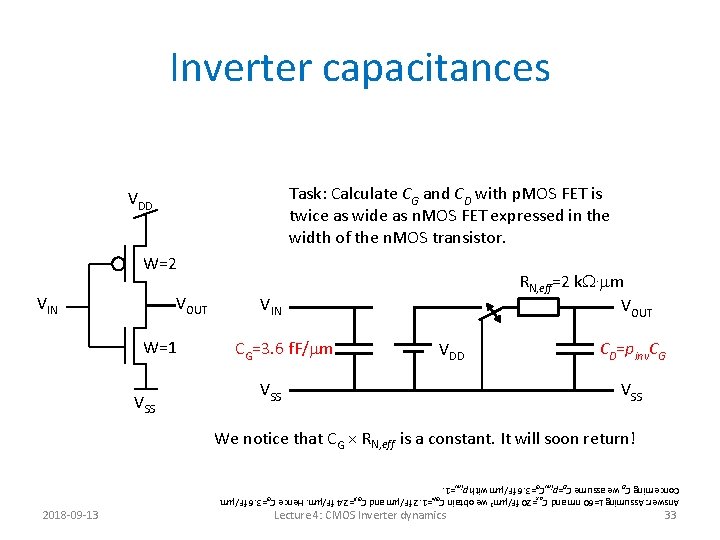
65 nm CMOS capacitances Gate capacitance Plate capacitance between gate and channel (but here we model it between gate and source) CG=WLCox LD W LS September 2018 Cox≈20 f. F/μm 2 (corresponds to 1. 2 nm effective oxide thickness, channel t ) length, L ox 60 nm effective channel length yields: CG=1. 2 f. F/μm Drain/source parasitic capacitances Same order of magnitude as the gate capacitance, CS=CD=pinv. CG Generic approach is to use pinv=1 for simplicity But sometimes pinv=0. 5 or pinv=0. 8! MCC 092 - The MOSFET 24

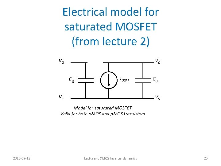
Electrical model for saturated MOSFET (from lecture 2) VG VD CG IDSAT VS CD VS Model for saturated MOSFET Valid for both n. MOS and p. MOS transistors 2018 -09 -13 Lecture 4: CMOS Inverter dynamics 25

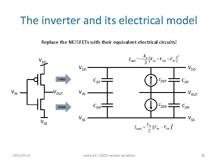
The inverter and its electrical model Replace the MOSFETs with their equivalent electrical circuits! VDD CGP PMOS VIN VOUT 2018 -09 -13 IDSP VIN CDP VOUT CGN NMOS VSS VDD VSS Lecture 4: CMOS Inverter dynamics IDSN CDN VSS 26

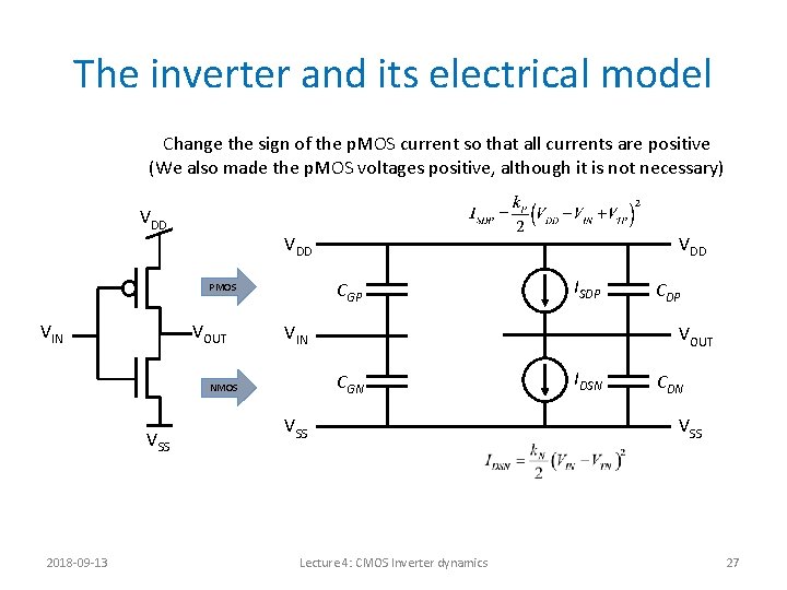
The inverter and its electrical model Change the sign of the p. MOS current so that all currents are positive (We also made the p. MOS voltages positive, although it is not necessary) VDD CGP PMOS VIN VOUT 2018 -09 -13 ISDP VIN CDP VOUT CGN NMOS VSS VDD VSS Lecture 4: CMOS Inverter dynamics IDSN CDN VSS 27

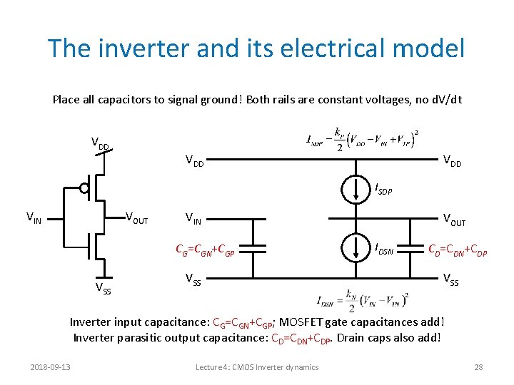
The inverter and its electrical model Place all capacitors to signal ground! Both rails are constant voltages, no d. V/dt VDD VDD ISDP VIN VOUT VIN CG=CGN+CGP VSS VOUT IDSN CD=CDN+CDP VSS Inverter input capacitance: CG=CGN+CGP; MOSFET gate capacitances add! Inverter parasitic output capacitance: CD=CDN+CDP. Drain caps also add! 2018 -09 -13 Lecture 4: CMOS Inverter dynamics 28

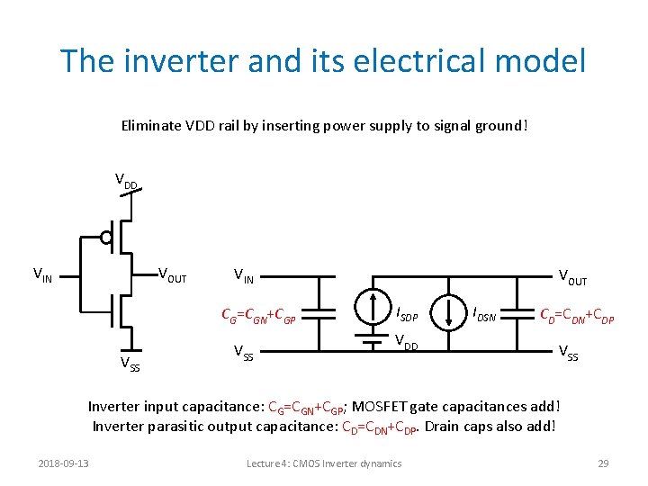
The inverter and its electrical model Eliminate VDD rail by inserting power supply to signal ground! VDD VIN VOUT VIN CG=CGN+CGP VSS VOUT ISDP VDD IDSN CD=CDN+CDP VSS Inverter input capacitance: CG=CGN+CGP; MOSFET gate capacitances add! Inverter parasitic output capacitance: CD=CDN+CDP. Drain caps also add! 2018 -09 -13 Lecture 4: CMOS Inverter dynamics 29

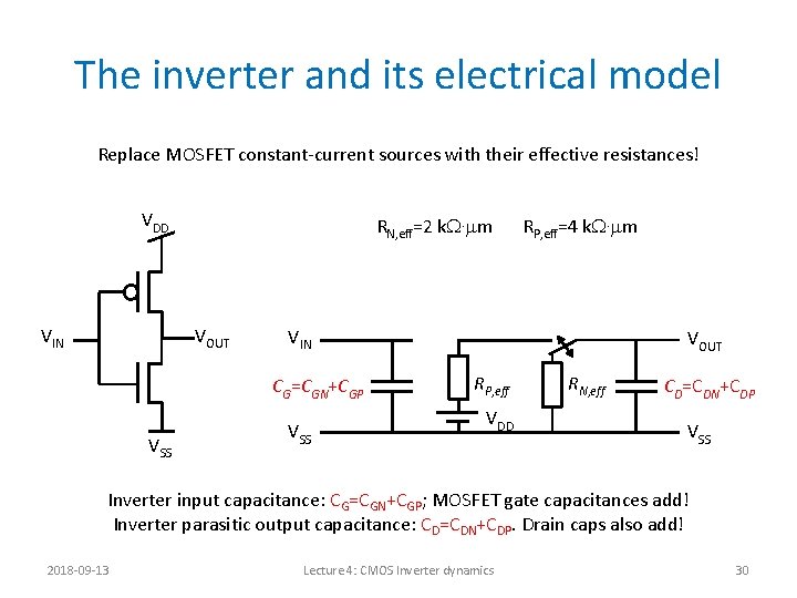
The inverter and its electrical model Replace MOSFET constant-current sources with their effective resistances! VDD VIN RN, eff=2 k. W. mm VOUT VIN CG=CGN+CGP VSS RP, eff=4 k. W. mm VSS VOUT RP, eff VDD RN, eff CD=CDN+CDP VSS Inverter input capacitance: CG=CGN+CGP; MOSFET gate capacitances add! Inverter parasitic output capacitance: CD=CDN+CDP. Drain caps also add! 2018 -09 -13 Lecture 4: CMOS Inverter dynamics 30

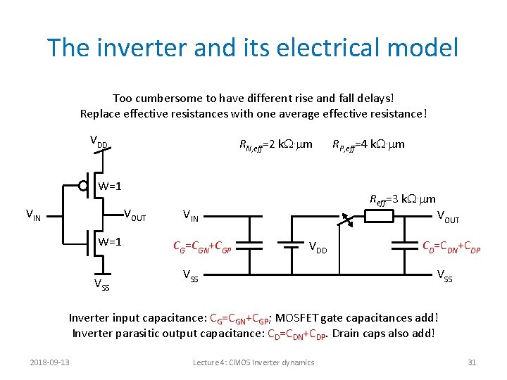
The inverter and its electrical model Too cumbersome to have different rise and fall delays! Replace effective resistances with one average effective resistance! VDD RN, eff=2 k. W. mm W=1 VIN VOUT W=1 VSS Reff=3 k. W. mm VIN CG=CGN+CGP RP, eff=4 k. W. mm VDD VSS VOUT CD=CDN+CDP VSS Inverter input capacitance: CG=CGN+CGP; MOSFET gate capacitances add! Inverter parasitic output capacitance: CD=CDN+CDP. Drain caps also add! 2018 -09 -13 Lecture 4: CMOS Inverter dynamics 31

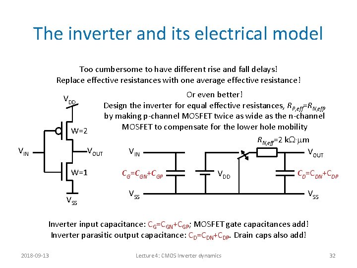
The inverter and its electrical model Too cumbersome to have different rise and fall delays! Replace effective resistances with one average effective resistance! Or even better! Design the inverter for equal effective resistances, RP, eff=RN, eff, by making p-channel MOSFET twice as wide as the n-channel MOSFET to compensate for the lower hole mobility W=2 RN, eff=2 k. W. mm VOUT VIN VOUT VDD VIN W=1 VSS CG=CGN+CGP VDD VSS CD=CDN+CDP VSS Inverter input capacitance: CG=CGN+CGP; MOSFET gate capacitances add! Inverter parasitic output capacitance: CD=CDN+CDP. Drain caps also add! 2018 -09 -13 Lecture 4: CMOS Inverter dynamics 32

Inverter capacitances Task: Calculate CG and CD with p. MOS FET is twice as wide as n. MOS FET expressed in the width of the n. MOS transistor. VDD W=2 VIN VOUT W=1 VSS RN, eff=2 k. W. mm VOUT VIN CG=3. 6 f. F/mm VDD VSS CD=pinv. CG VSS We notice that CG × RN, eff is a constant. It will soon return! Answer: Assuming L=60 nm and Cox=20 f. F/mm 2 we obtain CGN=1. 2 f. F/mm and CGP=2. 4 f. F/mm. Hence CG=3. 6 f. F/mm. Concerning CD we assume CD=pinv. CG=3. 6 f. F/mm with pinv=1. 2018 -09 -13 Lecture 4: CMOS Inverter dynamics 33

More than one inverter 2018 -09 -13 Lecture 4: CMOS Inverter dynamics 34

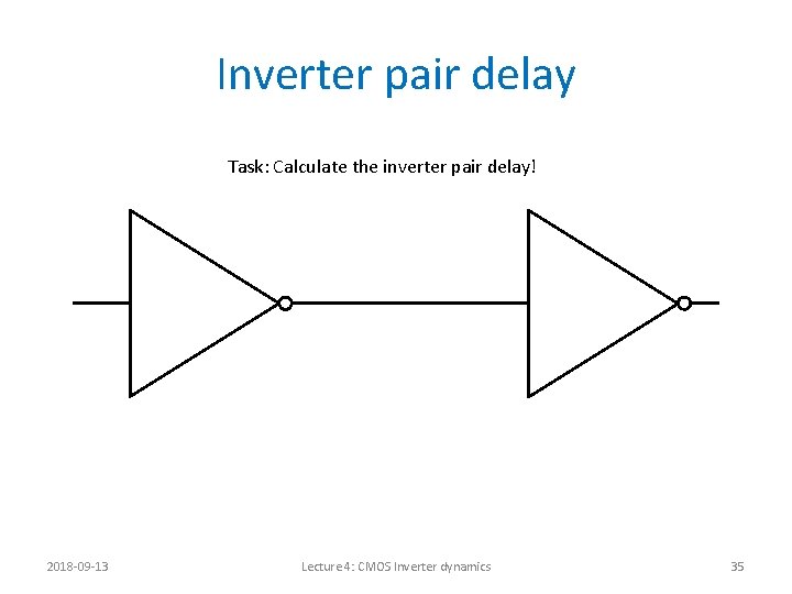
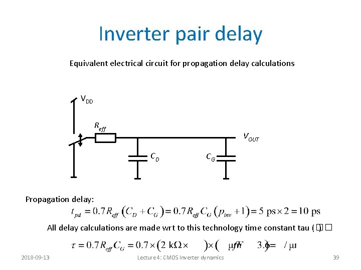
Inverter pair delay Task: Calculate the inverter pair delay! VDD Reff 2018 -09 -13 Lecture 4: CMOS Inverter dynamics 35

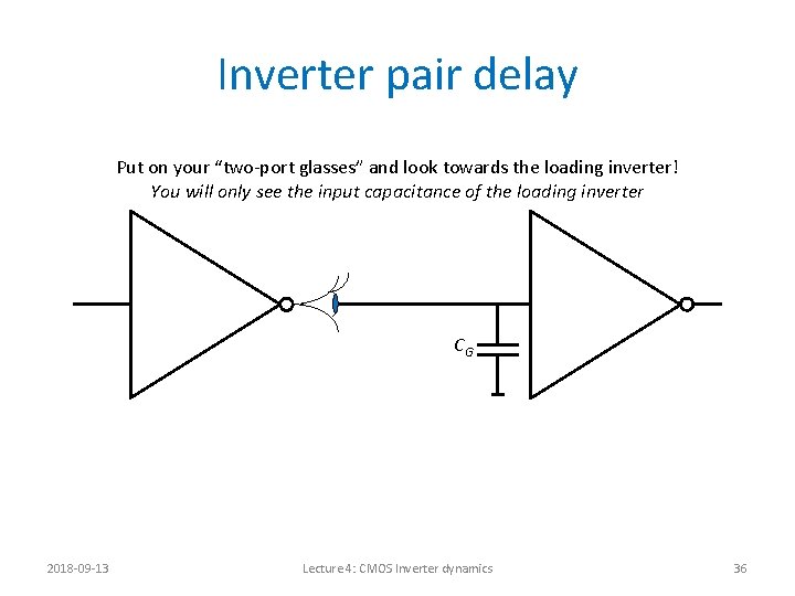
Inverter pair delay Put on your “two-port glasses” and look towards the loading inverter! You will only see the input capacitance of the loading inverter VDD Reff CG 2018 -09 -13 Lecture 4: CMOS Inverter dynamics 36

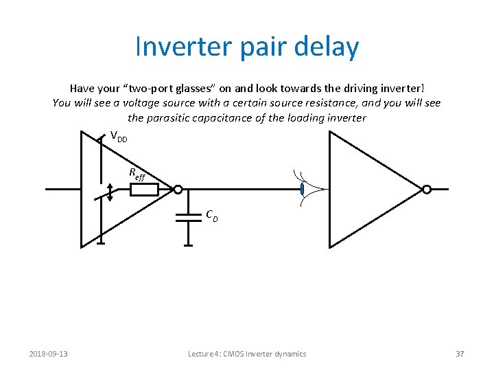
Inverter pair delay Have your “two-port glasses” on and look towards the driving inverter! You will see a voltage source with a certain source resistance, and you will see the parasitic capacitance of the loading inverter VDD Reff CD 2018 -09 -13 Lecture 4: CMOS Inverter dynamics 37

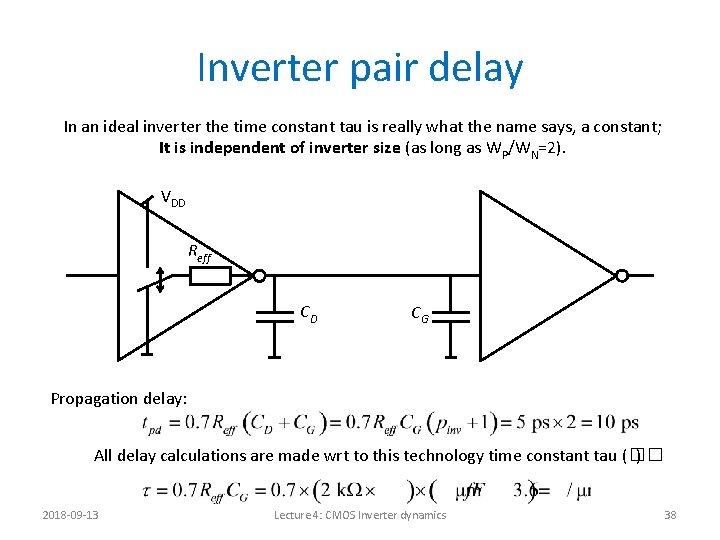
Inverter pair delay In an ideal inverter the time constant tau is really what the name says, a constant; It is independent of inverter size (as long as WP/WN=2). VDD Reff CD CG Propagation delay: All delay calculations are made wrt to this technology time constant tau (�� ) 2018 -09 -13 Lecture 4: CMOS Inverter dynamics 38

Inverter pair delay Equivalent electrical circuit for propagation delay calculations VDD Reff VOUT CD CG Propagation delay: All delay calculations are made wrt to this technology time constant tau (�� ) 2018 -09 -13 Lecture 4: CMOS Inverter dynamics 39

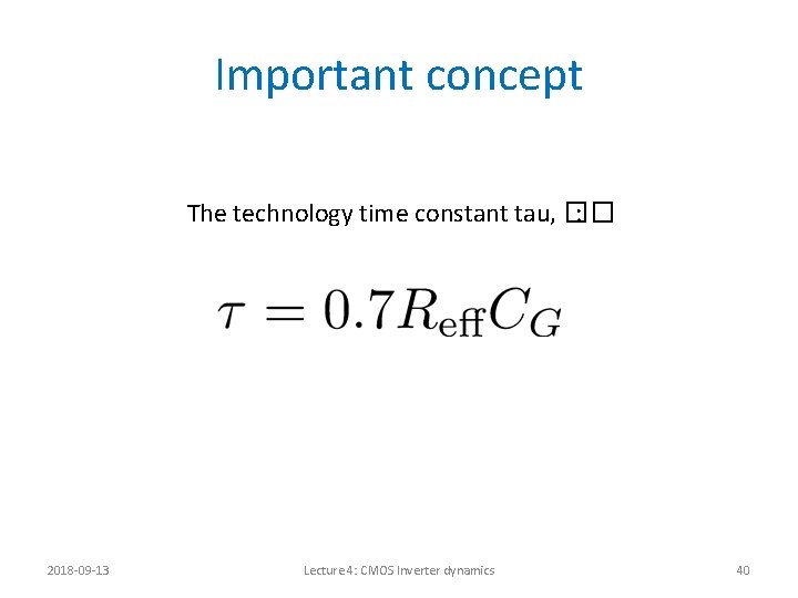
Important concept The technology time constant tau, �� : 2018 -09 -13 Lecture 4: CMOS Inverter dynamics 40

Quiz time! – Go to socrative. com – Select Student login – Go to room: “MCC 0922018” 2018 -09 -13 Lecture 4: CMOS Inverter dynamics 41

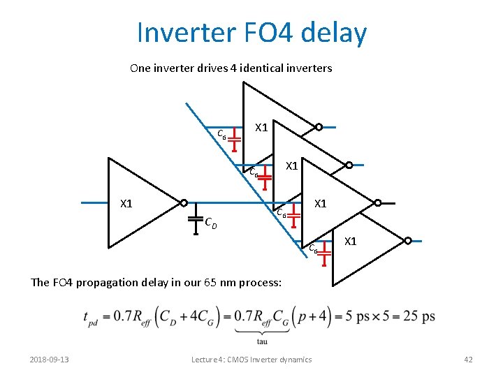
Inverter FO 4 delay One inverter drives 4 identical inverters CG VDD X 1 X 1 CG Reff CD X 1 CG CG X 1 The FO 4 propagation delay in our 65 nm process: 2018 -09 -13 Lecture 4: CMOS Inverter dynamics 42

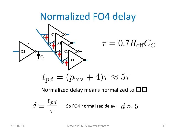
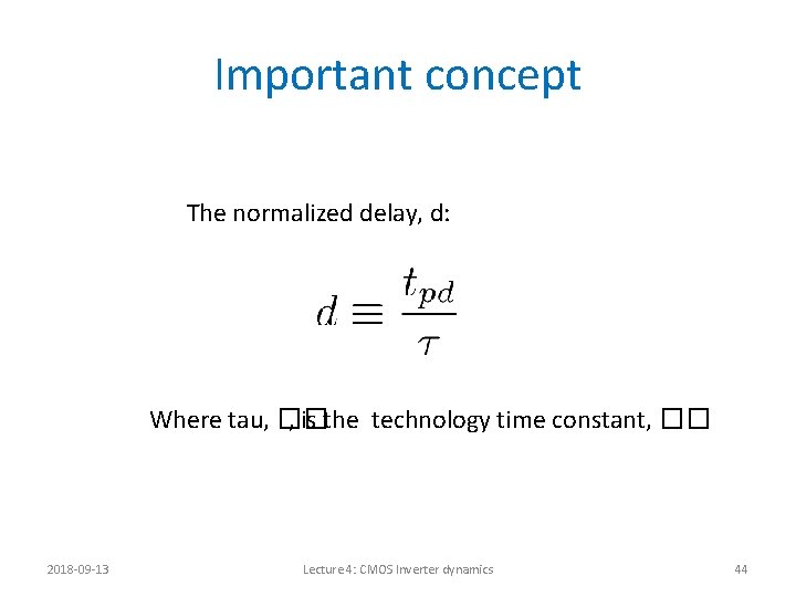
Normalized FO 4 delay VDD X 1 Reff CG X 1 CG CD X 1 CG X 1 Normalized delay means normalized to �� So FO 4 normalized delay: 2018 -09 -13 Lecture 4: CMOS Inverter dynamics 43

Important concept The normalized delay, d: Where tau, �� , is the technology time constant, �� 2018 -09 -13 Lecture 4: CMOS Inverter dynamics 44

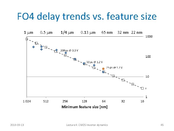
FO 4 delay trends vs. feature size 1 mm 2018 -09 -13 0. 5 mm 1/4 mm 0. 13 mm 65 nm Lecture 4: CMOS Inverter dynamics 32 nm 22 nm 45

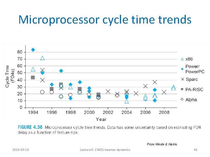
Microprocessor cycle time trends From Weste & Harris. 2018 -09 -13 Lecture 4: CMOS Inverter dynamics 46

Inverter Size • In most vendor cell libraries, inverters and other logic gates come in a number of different varieties concerning their driving capability (Reff) and input capacitance (CG). • In the following all inverters and logic gates of a certain size, e. g. size X=8, will have the same input capacitance, and, as an example, this input capacitance will be only half the input capacitance of a gate of size X=16. 2018 -09 -13 Lecture 4: CMOS Inverter dynamics 47

Minimizing delay through multiple inverters 2018 -09 -13 Lecture 4: CMOS Inverter dynamics 48

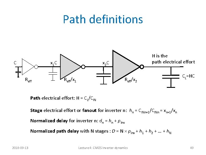
Path definitions C x 1 C Reff H is the path electrical effort x 2 C Reff/x 1 Reff/x 2 CL=HC Path electrical effort: H = CL/CIN Stage electrical effort or fanout for inverter n: hn = CINn+1/CINn = xn+1/xn Normalized delay for inverter n: dn = hn + pinv Normalized path delay with N stages : D = N × pinv + h 1 + h 2 + … + h. N 2018 -09 -13 Lecture 4: CMOS Inverter dynamics 49

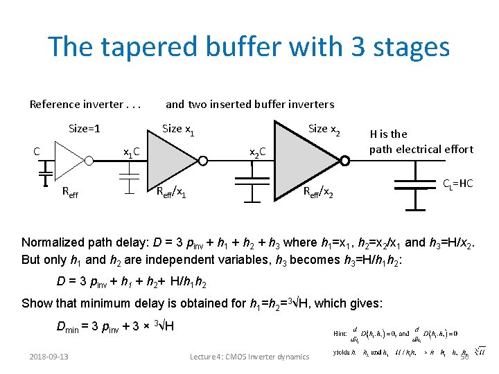
The tapered buffer with 3 stages Reference inverter. . . Size=1 C and two inserted buffer inverters Size x 1 C Reff Size x 2 C Reff/x 1 H is the path electrical effort Reff/x 2 CL=HC Normalized path delay: D = 3 pinv + h 1 + h 2 + h 3 where h 1=x 1, h 2=x 2/x 1 and h 3=H/x 2. But only h 1 and h 2 are independent variables, h 3 becomes h 3=H/h 1 h 2: D = 3 pinv + h 1 + h 2+ H/h 1 h 2 Show that minimum delay is obtained for h 1=h 2=3√H, which gives: Dmin = 3 pinv + 3 × 3√H 2018 -09 -13 Lecture 4: CMOS Inverter dynamics 50

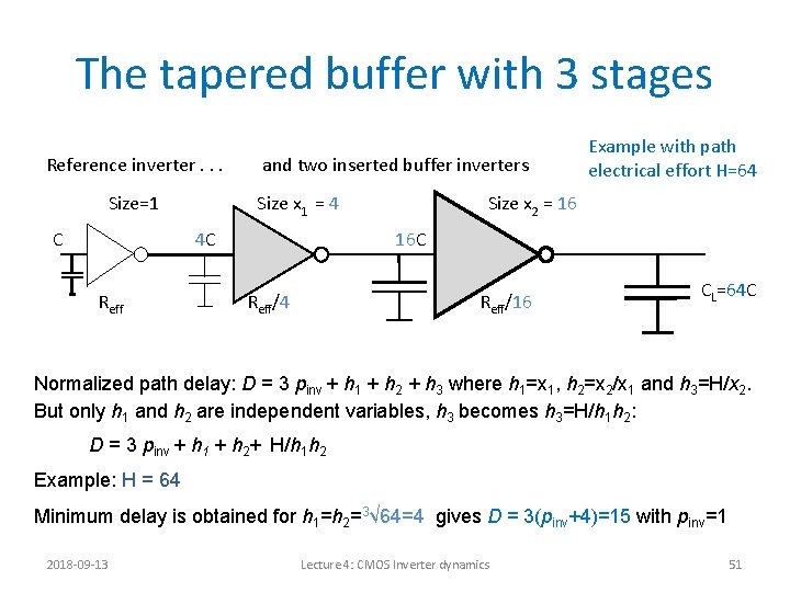
The tapered buffer with 3 stages Reference inverter. . . Size=1 C and two inserted buffer inverters Size x 1 = 4 4 C Reff Example with path electrical effort H=64 Size x 2 = 16 16 C Reff/4 Reff/16 CL=64 C Normalized path delay: D = 3 pinv + h 1 + h 2 + h 3 where h 1=x 1, h 2=x 2/x 1 and h 3=H/x 2. But only h 1 and h 2 are independent variables, h 3 becomes h 3=H/h 1 h 2: D = 3 pinv + h 1 + h 2+ H/h 1 h 2 Example: H = 64 Minimum delay is obtained for h 1=h 2=3√ 64=4 gives D = 3(pinv+4)=15 with pinv=1 2018 -09 -13 Lecture 4: CMOS Inverter dynamics 51

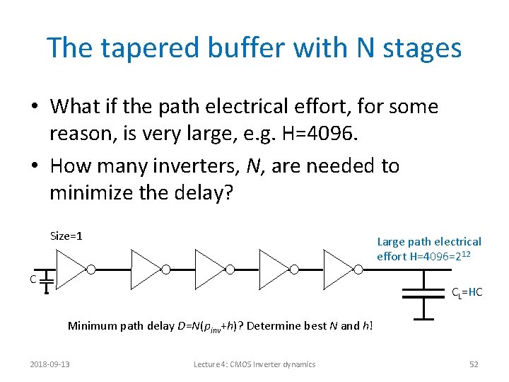
The tapered buffer with N stages • What if the path electrical effort, for some reason, is very large, e. g. H=4096. • How many inverters, N, are needed to minimize the delay? Size=1 Large path electrical effort H=4096=212 C CL=HC Minimum path delay D=N(pinv+h)? Determine best N and h! 2018 -09 -13 Lecture 4: CMOS Inverter dynamics 52

Best h & N? • Optimal h with pinv=0 can be shown analytically to be h=e= 2. 72 for Nopt = ln(H) • With larger pinv numerical solution gives h≈4 – That is why the FO 4 delay is so important! • The minimum is, so a bit larger h does only increase delay marginally and substancially smaller area 2018 -09 -13 Lecture 4: CMOS Inverter dynamics 53

Quick question • If you were to design a tapered buffer where the load capacitance is 1500 times larger than the input capacitance, and you are not allowed to invert the signal, how many inverters would you choose? • What would be the resulting normalized delay for the buffer? 2018 -09 -13 Lecture 4: CMOS Inverter dynamics 54

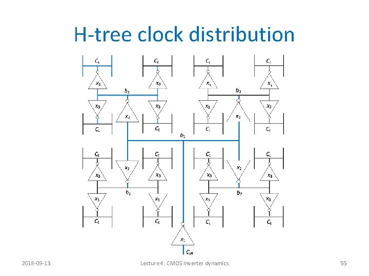
H-tree clock distribution 2018 -09 -13 Lecture 4: CMOS Inverter dynamics 55

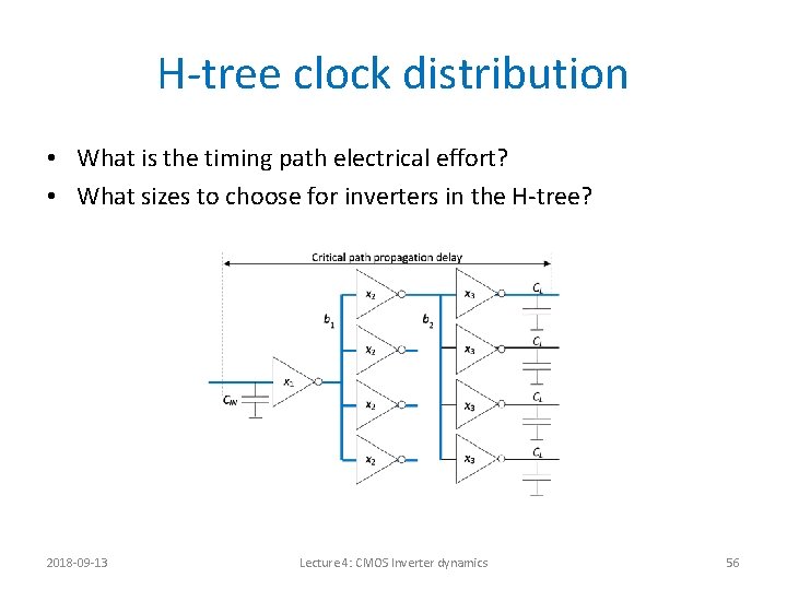
H-tree clock distribution • What is the timing path electrical effort? • What sizes to choose for inverters in the H-tree? 2018 -09 -13 Lecture 4: CMOS Inverter dynamics 56

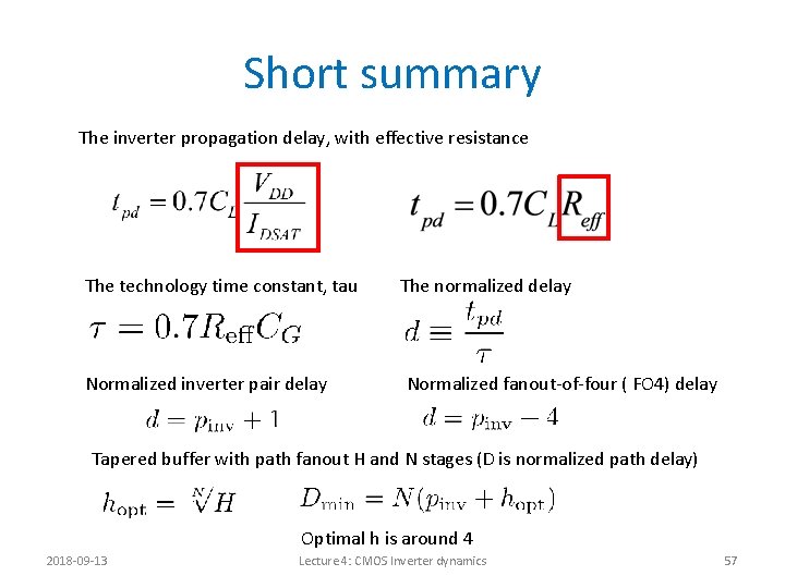
Short summary The inverter propagation delay, with effective resistance The technology time constant, tau Normalized inverter pair delay The normalized delay Normalized fanout-of-four ( FO 4) delay Tapered buffer with path fanout H and N stages (D is normalized path delay) Optimal h is around 4 2018 -09 -13 Lecture 4: CMOS Inverter dynamics 57

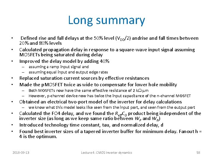
Long summary • • • Defined rise and fall delays at the 50% level (VDD/2) andrise and fall times between 20% and 80% levels Calculated propagation delay in response to a square-wave input signal assuming MOSFETs being saturated during delay Improved the delay model by adding 40% – assuming a ramp input signal and – assuming equal input and output edge rates • • Replaced saturation current sources by effective resistances Made the p. MOSFET twice as wide to compensate for lower hole mobility • Obtained an electrical two-port model of the inverter for delay calculations – Both MOSFETs now have the same effective resistance of 2 k. W. mm – However, p-channel device now has twice the input capacitance of the n-channel MOSFET – we know what this model looks like seen from the input port, and seen from the output port • • • Calculated the FO 4 delay, and we found the Reff. CG product being independent of the inverter size (as long as we keep same ratio between WP and WN) Introduced technology time constant, tau, and normalized delay, d Found best inverter sizes of a tapered inverter buffer for minimum delay. Fanout h = 4 is the optimum. 2018 -09 -13 Lecture 4: CMOS Inverter dynamics 58