Lecture 11 Dynamic CMOS Review Designing Fast CMOS
- Slides: 35

Lecture 11: Dynamic CMOS

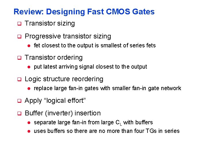
Review: Designing Fast CMOS Gates q Transistor sizing q Progressive transistor sizing l q Transistor ordering l q fet closest to the output is smallest of series fets put latest arriving signal closest to the output Logic structure reordering l replace large fan-in gates with smaller fan-in gate network q Apply “logical effort” q Buffer (inverter) insertion l l separate large fan-in from large CL with buffers uses buffers so there are no more than four TGs in series

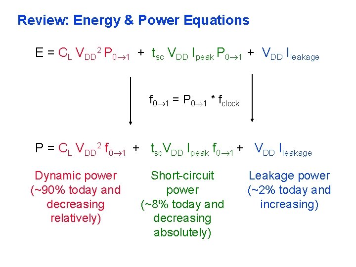
Review: Energy & Power Equations E = CL VDD 2 P 0 1 + tsc VDD Ipeak P 0 1 + VDD Ileakage f 0 1 = P 0 1 * fclock P = CL VDD 2 f 0 1 + tsc. VDD Ipeak f 0 1 + VDD Ileakage Dynamic power (~90% today and decreasing relatively) Short-circuit power (~8% today and decreasing absolutely) Leakage power (~2% today and increasing)

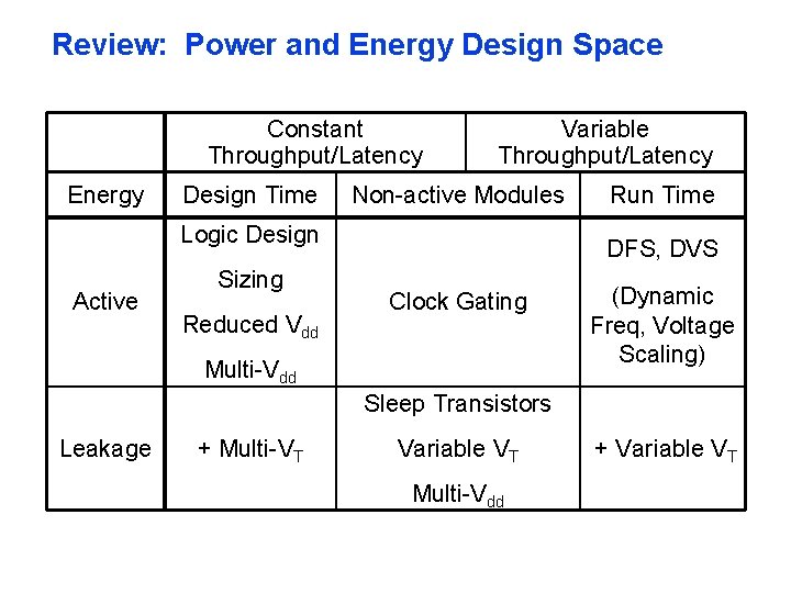
Review: Power and Energy Design Space Constant Throughput/Latency Energy Design Time Variable Throughput/Latency Non-active Modules Logic Design Active Sizing Reduced Vdd Run Time DFS, DVS Clock Gating Multi-Vdd (Dynamic Freq, Voltage Scaling) Sleep Transistors Leakage + Multi-VT Variable VT Multi-Vdd + Variable VT

Dynamic CMOS q In static circuits at every point in time (except when switching) the output is connected to either GND or VDD via a low resistance path. l q fan-in of N requires 2 N devices Dynamic circuits rely on the temporary storage of signal values on the capacitance of high impedance nodes. l l requires only N + 2 transistors takes a sequence of precharge and conditional evaluation phases to realize logic functions

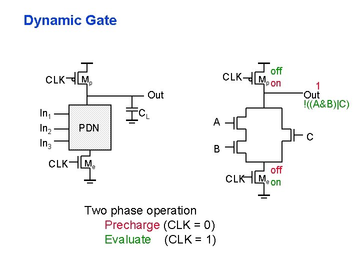
Dynamic Gate CLK Mp off Mp on Out In 1 In 2 In 3 CLK CL PDN 1 Out !((A&B)|C) A C B Me CLK Two phase operation Precharge (CLK = 0) Evaluate (CLK = 1) off Me on

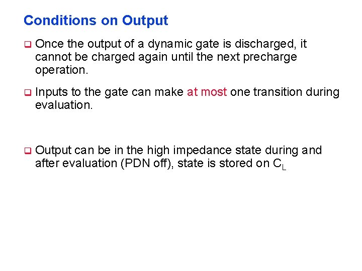
Conditions on Output q Once the output of a dynamic gate is discharged, it cannot be charged again until the next precharge operation. q Inputs to the gate can make at most one transition during evaluation. q Output can be in the high impedance state during and after evaluation (PDN off), state is stored on CL

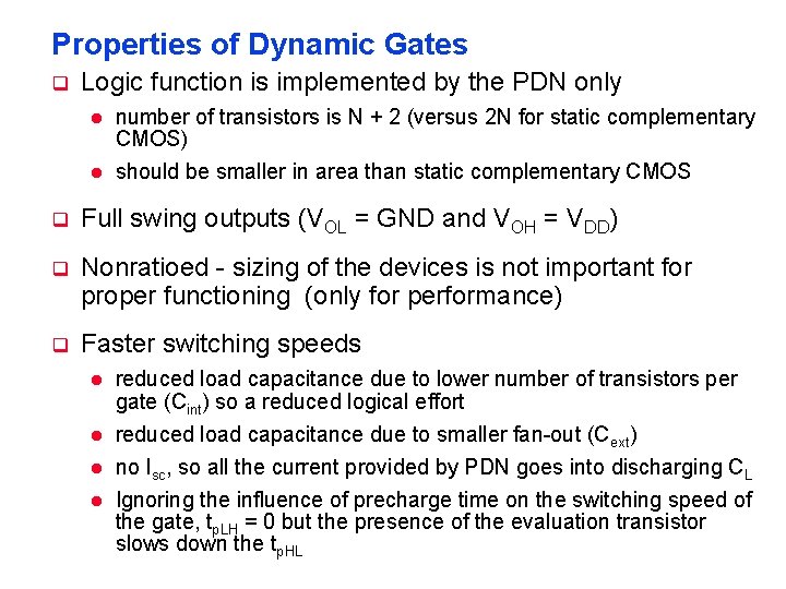
Properties of Dynamic Gates q Logic function is implemented by the PDN only l l number of transistors is N + 2 (versus 2 N for static complementary CMOS) should be smaller in area than static complementary CMOS q Full swing outputs (VOL = GND and VOH = VDD) q Nonratioed - sizing of the devices is not important for proper functioning (only for performance) q Faster switching speeds l l reduced load capacitance due to lower number of transistors per gate (Cint) so a reduced logical effort reduced load capacitance due to smaller fan-out (Cext) no Isc, so all the current provided by PDN goes into discharging CL Ignoring the influence of precharge time on the switching speed of the gate, tp. LH = 0 but the presence of the evaluation transistor slows down the tp. HL

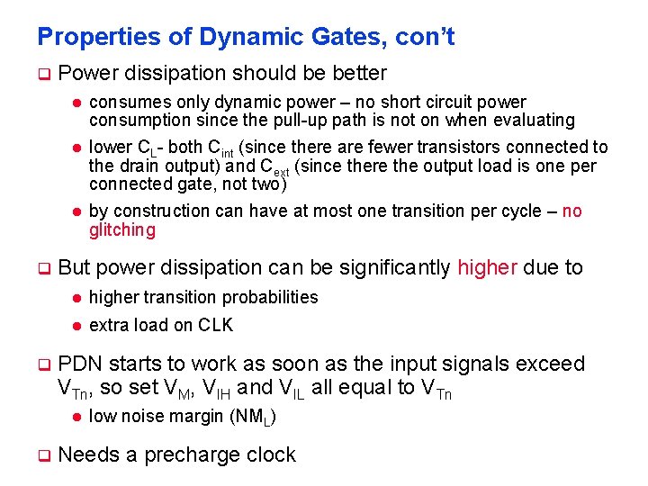
Properties of Dynamic Gates, con’t q Power dissipation should be better l l l q q by construction can have at most one transition per cycle – no glitching But power dissipation can be significantly higher due to l higher transition probabilities l extra load on CLK PDN starts to work as soon as the input signals exceed VTn, so set VM, VIH and VIL all equal to VTn l q consumes only dynamic power – no short circuit power consumption since the pull-up path is not on when evaluating lower CL- both Cint (since there are fewer transistors connected to the drain output) and Cext (since there the output load is one per connected gate, not two) low noise margin (NML) Needs a precharge clock

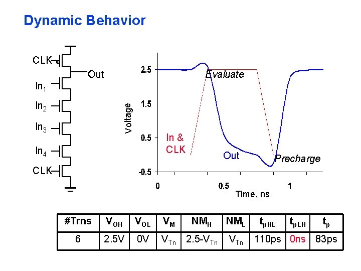
Dynamic Behavior CLK Out Evaluate In 1 Voltage In 2 In 3 In & CLK In 4 Out Precharge CLK Time, ns #Trns VOH VOL VM NMH NML 6 2. 5 V 0 V VTn 2. 5 -VTn tp. HL tp. LH tp 110 ps 0 ns 83 ps

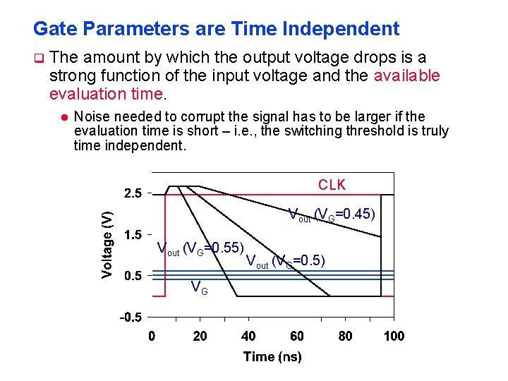
Gate Parameters are Time Independent q The amount by which the output voltage drops is a strong function of the input voltage and the available evaluation time. l Noise needed to corrupt the signal has to be larger if the evaluation time is short – i. e. , the switching threshold is truly time independent. CLK Vout (VG=0. 45) Vout (VG=0. 55) VG Vout (VG=0. 5)

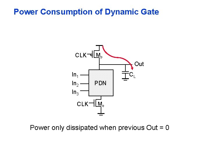
Power Consumption of Dynamic Gate CLK Mp Out In 1 In 2 In 3 CLK CL PDN Me Power only dissipated when previous Out = 0

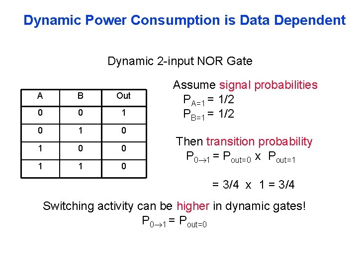
Dynamic Power Consumption is Data Dependent Dynamic 2 -input NOR Gate A B Out 0 0 1 0 1 0 0 1 1 0 Assume signal probabilities PA=1 = 1/2 PB=1 = 1/2 Then transition probability P 0 1 = Pout=0 x Pout=1 = 3/4 x 1 = 3/4 Switching activity can be higher in dynamic gates! P 0 1 = Pout=0

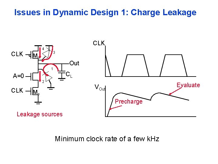
Issues in Dynamic Design 1: Charge Leakage CLK 4 Mp 3 Out 1 CL A=0 2 CLK Evaluate VOut Me Precharge Leakage sources Minimum clock rate of a few k. Hz

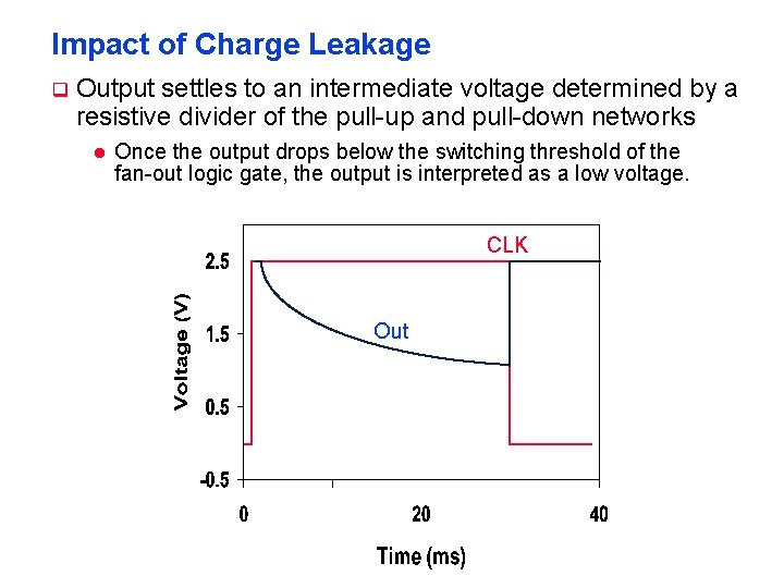
Impact of Charge Leakage q Output settles to an intermediate voltage determined by a resistive divider of the pull-up and pull-down networks l Once the output drops below the switching threshold of the fan-out logic gate, the output is interpreted as a low voltage. CLK Out

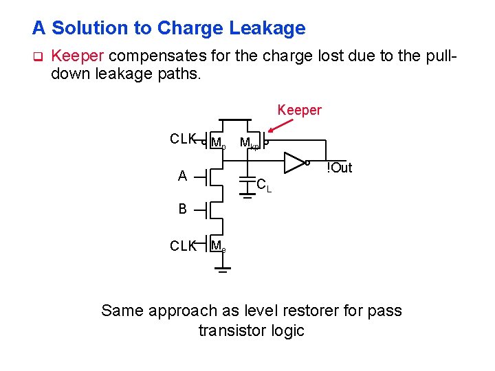
A Solution to Charge Leakage q Keeper compensates for the charge lost due to the pulldown leakage paths. Keeper CLK Mp Mkp !Out A CL B CLK Me Same approach as level restorer for pass transistor logic

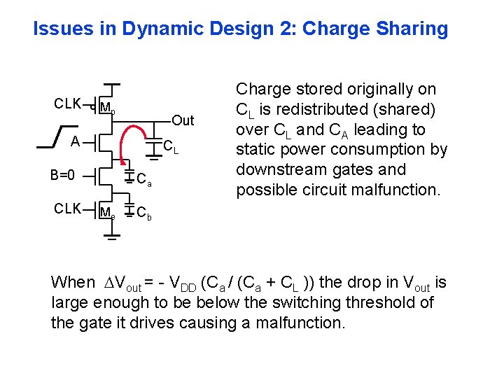
Issues in Dynamic Design 2: Charge Sharing CLK Mp Out A CL B=0 CLK Ca Me Charge stored originally on CL is redistributed (shared) over CL and CA leading to static power consumption by downstream gates and possible circuit malfunction. Cb When Vout = - VDD (Ca / (Ca + CL )) the drop in Vout is large enough to be below the switching threshold of the gate it drives causing a malfunction.

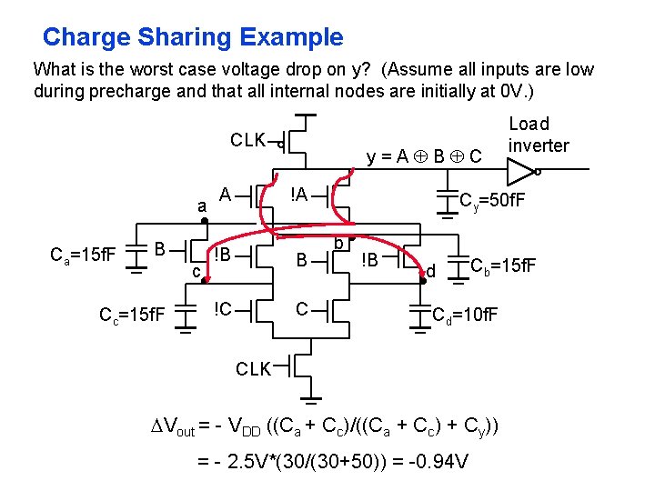
Charge Sharing Example What is the worst case voltage drop on y? (Assume all inputs are low during precharge and that all internal nodes are initially at 0 V. ) CLK a Ca=15 f. F B c Cc=15 f. F A y=A B C !A !B B !C C Load inverter Cy=50 f. F b !B d Cb=15 f. F Cd=10 f. F CLK Vout = - VDD ((Ca + Cc)/((Ca + Cc) + Cy)) = - 2. 5 V*(30/(30+50)) = -0. 94 V

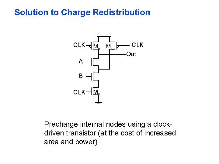
Solution to Charge Redistribution CLK Mp Mkp CLK Out A B CLK Me Precharge internal nodes using a clockdriven transistor (at the cost of increased area and power)

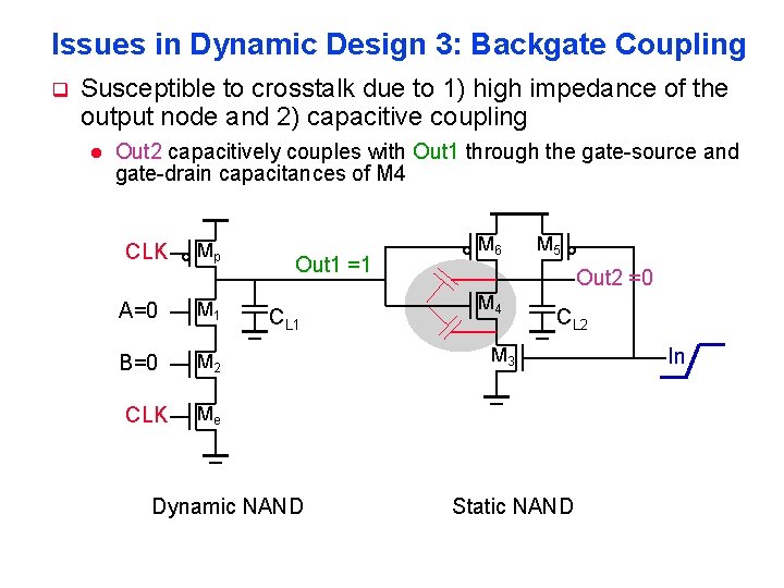
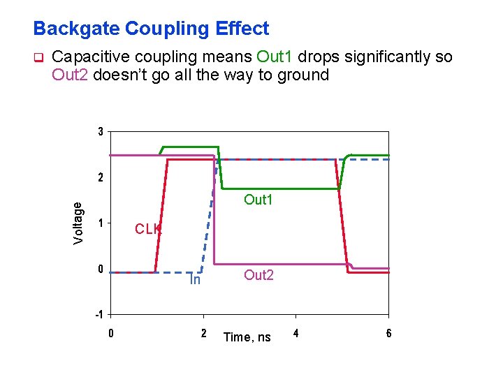
Issues in Dynamic Design 3: Backgate Coupling q Susceptible to crosstalk due to 1) high impedance of the output node and 2) capacitive coupling l Out 2 capacitively couples with Out 1 through the gate-source and gate-drain capacitances of M 4 CLK Mp A=0 M 1 B=0 M 2 CLK Out 1 =1 CL 1 M 6 M 5 Out 2 =0 M 4 CL 2 M 3 Me Dynamic NAND Static NAND In

Backgate Coupling Effect Capacitive coupling means Out 1 drops significantly so Out 2 doesn’t go all the way to ground Voltage q Out 1 CLK In Out 2 Time, ns

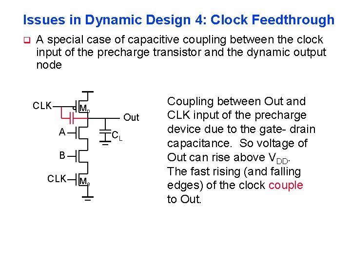
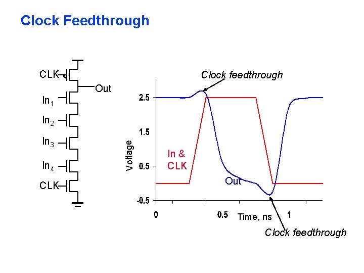
Issues in Dynamic Design 4: Clock Feedthrough q A special case of capacitive coupling between the clock input of the precharge transistor and the dynamic output node CLK Mp A CL B CLK Out Me Coupling between Out and CLK input of the precharge device due to the gate- drain capacitance. So voltage of Out can rise above VDD. The fast rising (and falling edges) of the clock couple to Out.

Clock Feedthrough CLK Clock feedthrough Out In 1 In 3 In 4 CLK Voltage In 2 In & CLK Out Time, ns Clock feedthrough

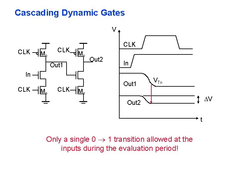
Cascading Dynamic Gates V CLK Mp Out 1 Out 2 In In CLK Me CLK Out 1 VTn Me V Out 2 t Only a single 0 1 transition allowed at the inputs during the evaluation period!

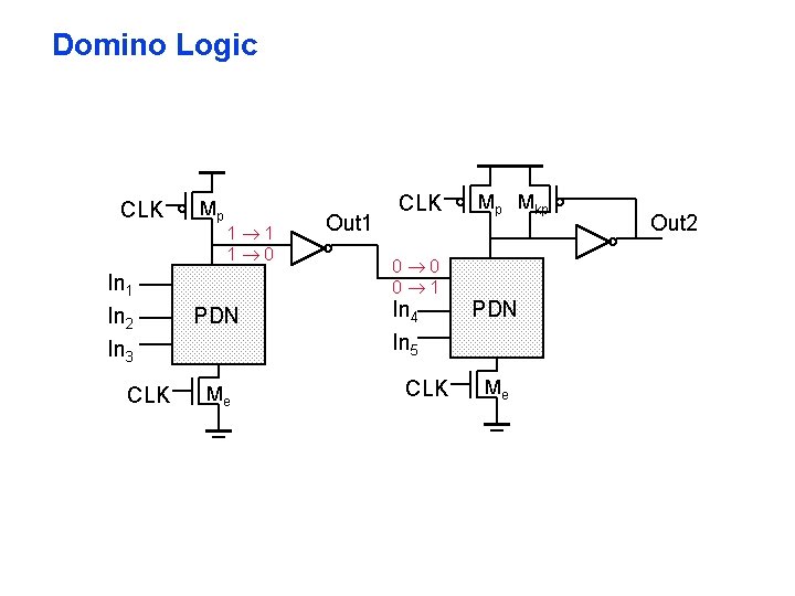
Domino Logic CLK In 1 In 2 In 3 CLK Mp 1 1 1 0 PDN Me Out 1 CLK 0 0 0 1 In 4 In 5 CLK Mp Mkp PDN Me Out 2

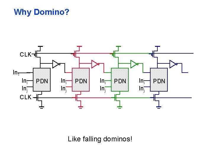
Why Domino? CLK In 1 Ini PDN Inj CLK Ini Inj PDN Like falling dominos! Ini Inj PDN

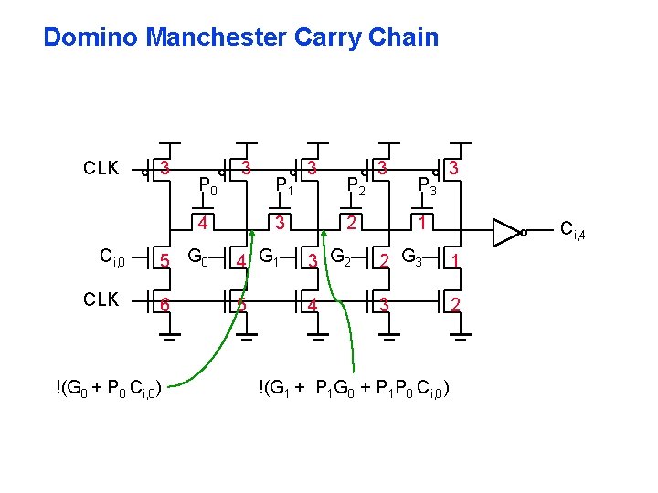
Domino Manchester Carry Chain CLK 3 P 0 3 4 Ci, 0 CLK P 1 3 3 P 2 3 2 P 3 3 1 Ci, 4 5 G 0 4 G 1 3 G 2 2 G 3 1 6 5 4 3 2 !(G 0 + P 0 Ci, 0) !(G 1 + P 1 G 0 + P 1 P 0 Ci, 0)

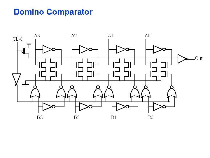
Domino Comparator CLK A 3 A 2 A 1 A 0 Out B 3 B 2 B 1 B 0

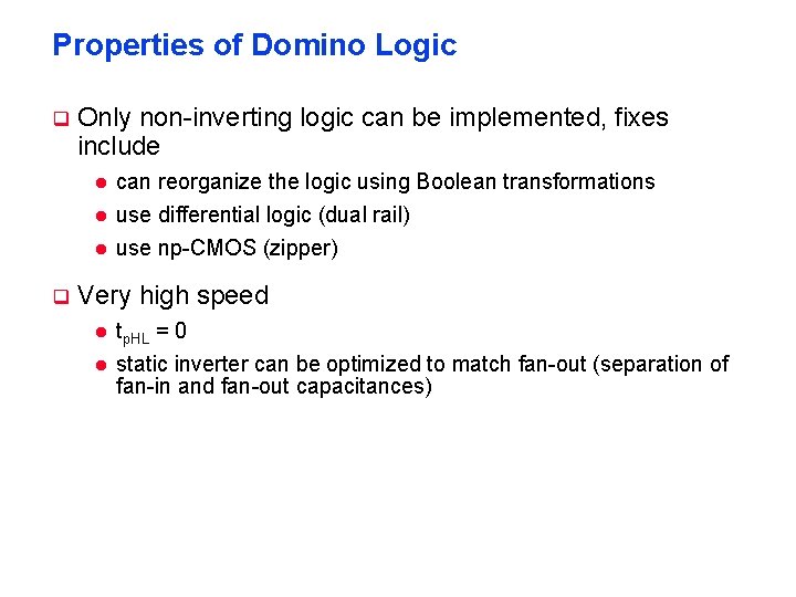
Properties of Domino Logic q Only non-inverting logic can be implemented, fixes include l can reorganize the logic using Boolean transformations use differential logic (dual rail) l use np-CMOS (zipper) l q Very high speed l tp. HL l =0 static inverter can be optimized to match fan-out (separation of fan-in and fan-out capacitances)

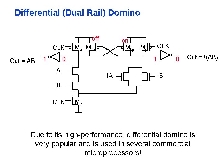
Differential (Dual Rail) Domino off CLK Out = AB 1 on Mp Mkp 0 CLK Mp 0 !Out = !(AB) 1 A !A !B B CLK Me Due to its high-performance, differential domino is very popular and is used in several commercial microprocessors!

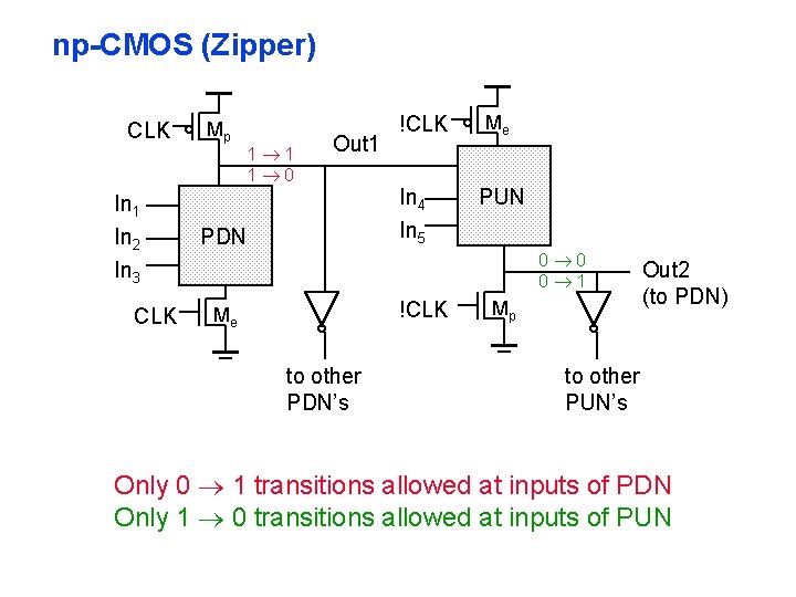
np-CMOS (Zipper) CLK In 1 In 2 In 3 CLK Mp 1 1 1 0 Out 1 PDN !CLK In 4 In 5 Me PUN 0 0 0 1 !CLK Me to other PDN’s Mp Out 2 (to PDN) to other PUN’s Only 0 1 transitions allowed at inputs of PDN Only 1 0 transitions allowed at inputs of PUN

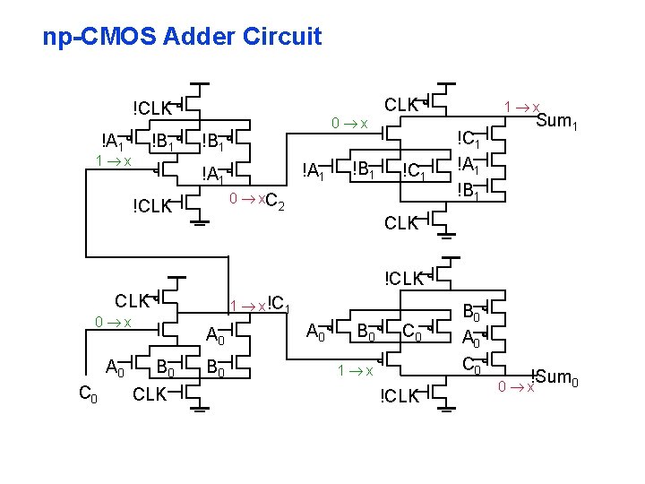
np-CMOS Adder Circuit !CLK !A 1 !B 1 1 x 0 x !B 1 !A 1 0 x. C !CLK !B 1 2 CLK !C 1 1 x Sum 1 !C 1 !A 1 !B 1 CLK !CLK 1 x!C 1 0 x A 0 C 0 A 0 B 0 CLK B 0 A 0 B 0 C 0 1 x !CLK B 0 A 0 C 0 !Sum 0 0 x

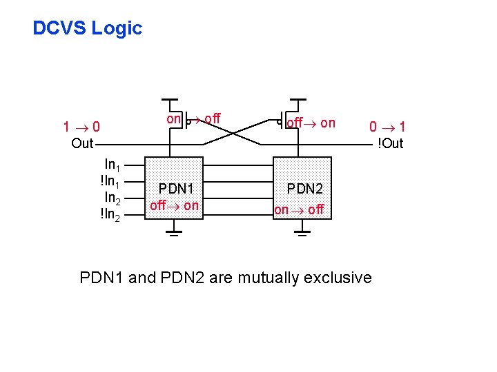
DCVS Logic 1 0 Out In 1 !In 1 In 2 !In 2 on off PDN 1 off on off on 0 1 !Out PDN 2 on off PDN 1 and PDN 2 are mutually exclusive

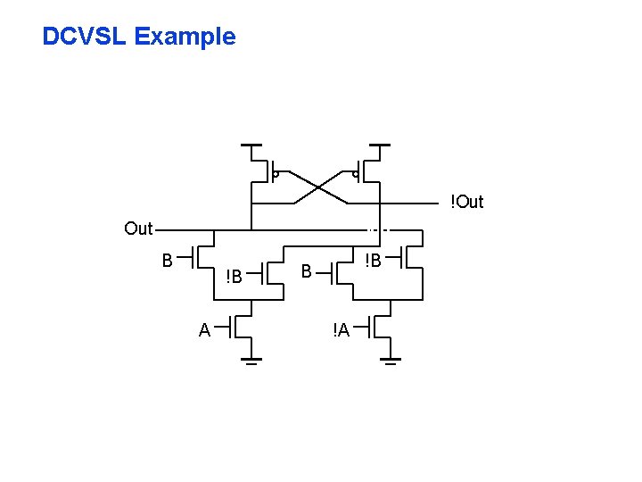
DCVSL Example !Out B !B A !B B !A

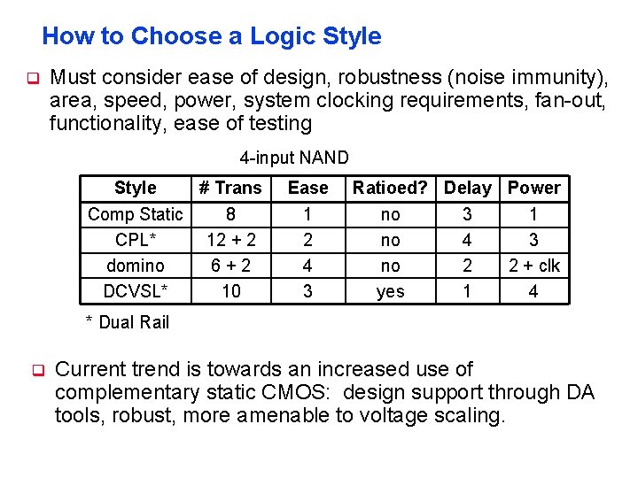
How to Choose a Logic Style q Must consider ease of design, robustness (noise immunity), area, speed, power, system clocking requirements, fan-out, functionality, ease of testing 4 -input NAND Style # Trans Comp Static 8 CPL* 12 + 2 domino 6+2 DCVSL* 10 Ease 1 2 4 3 Ratioed? Delay Power no 3 1 no 4 3 no 2 2 + clk yes 1 4 * Dual Rail q Current trend is towards an increased use of complementary static CMOS: design support through DA tools, robust, more amenable to voltage scaling.