Basic Logic Gates and Truth Tables NOT Inverter
 F = A. B NAND F")
Basic Logic Gates and Truth Tables NOT (Inverter) F = A. B NAND F = A+B NOR AND F = A+B OR

Basic Logic Gates and Truth Tables

Introduction to Field Programmable Gate Arrays

Introduction to Field Programmable Gate Arrays The first FPGAs for Xilinx in 1985 using a very mature 1. 2 m process consists of 1, 000 ASIC gate equivalent running at 18 MHZ. https: //anysilicon. com/fpga-vs-asic-choose/

Introduction to Field Programmable Gate Arrays

FPGA Design Flow Overview The ISE® design flow comprises the following steps: design entry, design synthesis, design implementation, and Xilinx® device programming. Design verification, which includes both functional verification and timing verification, takes places at different points during the design flow. This section describes what to do during each step. For additional details on each design step, click on a link below the following figure. https: //www. xilinx. com/support/documentation/sw_manuals/xilinx 10/isehelp/ise_c_fpga_design_flow_overview. htm

difference between logical and bit-wise operator Suppose A=3′b 101, B=3′b 010. Logical AND: Y=A&&B means if A is true(non-zero) and B(non-zero) is true Y will get ‘ 1’ else ‘ 0′. So here Y=1. Bit-wise AND: Y=A&B means bit-wise and operation of A, B. So here Y=3′b 000. Logical OR: Y=A||B means if any of these two true i. e. A is true(non-zero) or B(non-zero) is true Y will get ‘ 1’ else if both are false(Zero) then ‘ 0′. So here Y=1; Bit-wise OR: Y=A|B means bit-wise ‘or’ operation of A, B. So here Y=3′b 111. But the trick is with NOT operation. Logical NOT: Y=!B means if B is true(non-zero) Y will get false i. e. ‘ 0’ else ‘ 1′. So here Y=0. Bit-wise NOT: Y=~B means bit-wise complement operation of B. So here Y=3′b 101.

Precedence of Operations in Verilog Highest Lowest == tests for only 1 and 0, while === tests for 1, 0, X, Z. Verilog HDL operators can be divided into several groups

1/1 00 1/1 11 0/1 1/0 01 0/0 Current St Q 1 Q 0 Input In Next St Q 1+Q 0+ Output Out 00 0 01 1 00 1 01 0 10 0 01 1 11 0 10 0 11 0 10 1 11 0 01 1 11 1 00 1 0/0 1/1 10 Q 1’Q 0 + Q 1 Q 0’ CLK 1 1 Out = In. Q 0 + Q 1’Q 0’ + Q 1 Q 0 In’Q 0’ + In’Q 1 + In. Q 1’Q 0 0 0 In Q 1 Q 0 00 0 0 1 0 01 1 11 0 10 1 1 0 1 Q 1+ = Q 1’Q 0 + Q 1 Q 0’ Q 1 Q 0 In 00 0 1 1 0 01 0 11 1 10 1 1 0 0 Q 0+ = In’Q 0’ + In’Q 1 + In. Q 1’Q 0 Q 1 Q 0 In 00 01 11 10 1 0 1 Out = In. Q 0 + Q 1’Q 0’ + Q 1 Q 0

Examples to complete two_input_xor: // example 1 assign out = in 1 ^ in 2; // example 2 wire product 1, product 2; assign product 1 = in 1 && !in 2; assign product 2 = !in 1 && in 2; assign out = product 1 || product 2; // example 3 assign out = (in 1 != in 2); // example 4 assign out = in 1 ? (!in 2) : (in 2); // could have done in // single assignment // statement…
 module mux_2")
// Behavioral Model of a 2 to 1 MUX (16 data inputs) module mux_2 to 1(Y, A, B, sel); output [15: 0] Y; input [15: 0] A, B; input sel; reg [15: 0] Y; always @(A or B or sel) if (sel == 1'b 0) Y = A; else Y = B; endmodule // Behavioral Model of a 4 to 1 MUX (16 data inputs) module mux_4 to 1(Y, A, B, C, D, sel); output [15: 0] Y; input [15: 0] A, B, C, D; input [1: 0] sel; reg [15: 0] Y; always @(A or B or C or D or sel) case ( sel ) 2'b 00: Y = A; 2'b 01: Y = B; 2'b 10: Y = C; 2'b 11: Y = D; default: Y = 16'hxxxx; endcase endmodule

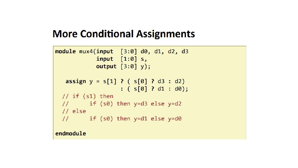
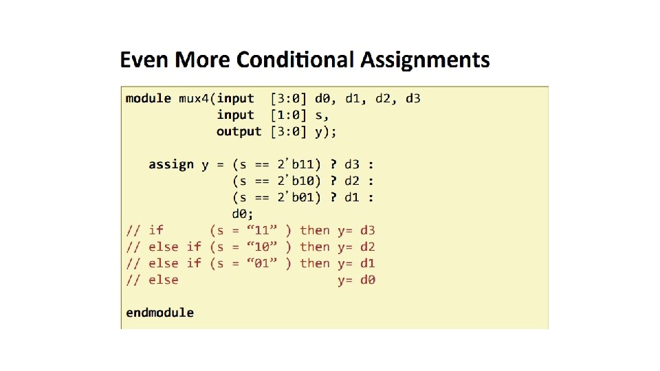
2 -bit MUX examples Using if Statement Using assign Statement http: //www. asic-world. com/examples/verilog/mux. html Using case Statement

http: //euler. ecs. umass. edu/ece 232/pdf/03 -verilog-11. pdf

Sample Test Questions


Synthesis of Combinational Logic – Gate Netlist Synthesis tools further optimize a gate netlist in term of Verilog primitives. Example: Given the pre-synthesized circuit below, write the Verilog, optimize circuit using only 2 -input gates (Optimized) cs. haifa. ac. il/courses/verilog_tutorial 2. ppt

http: //www. syssec. ethz. ch/content/dam/ethz/special-interest/infk/inst-infsec/system-security-groupdam/education/Digitaltechnik_14/07_Verilog_Combinational. pdf

Structural Modeling of Sequential Circuits // Mixed Structural and Dataflow module Seq_Circuit_Structure (input In, CLK, output Out); wire D 0, D 1, Q 0 b, Q 1 b; // Instantiate two D Flip-Flops D_FF FF 0(D 0, CLK, Q 0 b); D_FF FF 1(D 1, CLK, Q 1 b); // Modeling logic assign D 0 = Q 1 b & In; assign D 1 = (Q 0 & ~In) | (Q 1 & ~In); assign Out = Q 0 & Q 1; endmodule

- Slides: 28