Solar MPPT Pure Sine Inverter Design Overview v


- Slides: 34
Solar MPPT Pure Sine Inverter
Design Overview v The solar inverter is a critical component in a solar energy system. v At the heart of the system is a -time microcontroller. real v It is programmed to perform the control loops necessary for all the power management functions v The controller also maximizes the power output from the PV through MPPT algorithm.
Conventional Solar MPPT system Solar MPPT Pure Sine inverter
Need for Maximum power point tracking q Photovoltaic cells have a complex relationship between their operating environment and the maximum power produced. q Graph shows solar cell I-V curves where a line intersects the knee of the curves where the maximum power point is located. q The PV maximum output power is dependent on the operating conditions of the panel.
Perturb and observe tracking algorithm P-V and I-V curve of solar cell Perturb and Observe Method § In this method, the controller adjusts the voltage by a small amount from the array and measures power § It is referred to as a hill climbing method, because it depends on the rise of the curve of power against voltage below the maximum power point, and the fall above that point.
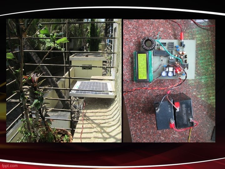
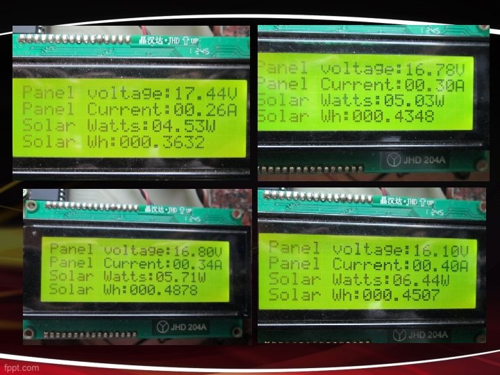
DC-DC Buck Converter – MPPT Charge controller Mosfet used as a switching device. PWM duty cycle D varied according to MPPT algorithm. Converter output charges battery. If there is excess voltage available from the PV, then it converts that to additional current to the battery. Vout = D x Vin Solar panel DC DC converter Storage battery
Panel Voltage switch ON switch OFF
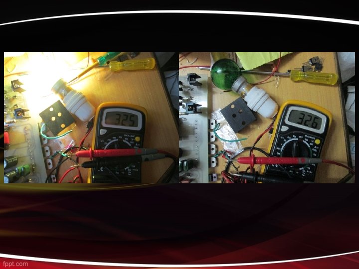
How to make 230 V AC from 12/24 V DC efficiently ? … well without the transformer being bulky and noisy Generate 50 Hz AC from 12/24 V DC Generate 12/24 v AC @80 Khz from 12/24 v DC Step up to 325 v AC @80 Khz using a HF ferrite transformer Step up to 230 V AC using a 50 Hz conventional transformer Rectify & filter 325 v AC to get 325 v DC Shape 50 Hz wave from 325 v DC to get Vrms 230 v@50 Hz
Push Pull converter - HVDC generation using SG 3525 SMPS controller Ø SG 3525 is a single package multi function SMPS controller IC Ø Switching frequencies between 10 KHz to 500 KHz can be used Ø Step up with a high frequency transformer Ø Convert back to DC with simple rectifiers Ø Feedback for output regulation Ø Softstart for gradually loading the transformer Ø Direct Mosfet Gate drive
HVDC generation
High Frequency transformer …What makes them slim? Flux density, which is the key design factor of a transformer, is a function of both cross sectional area of the core and frequency Bmax = Vrms× 108/4. 44 N×Ac×F Bmax = Vpk× 108/4 N×Ac×F In this equations: V - voltage (volts) Ac - core's cross-sectional area (sq. cm) for sine waves for square waves N - winding's turns F- frequency (hertz) v Desired flux density can be achieved by reducing the cross sectional area of the core but increasing the frequency v For a given wattage, the ferrite core HF transformers operate with lower flux densities than the Iron core transformers
High Frequency transformer Higher frequency transformers are smaller and lighter compared to their 50 Hz counterparts Before After
High side 1 Low side 1 High side 2 USPWM - Unipolar Sinusoidal Pulse Width Modulation Ø USPWM signals generated by MCU Ø Use of single VDD Low side 2 Ø Carrier PWM @ 62. 5 Khz Output Ø Sine look up table is used to modulate PWM
50 Hz Sine wave shape using PWM § High voltage MOSFETs or IGBTs are used for the switching bridge § The bridge arms are 180 o out of phase. § Pairs Q 1 -Q 3 & Q 2 -Q 4 conduct at a time 360 V DC Ø Dead time provided in code to avoid shoot-through condition § Gate drive circuitry has to be isolated from the digital circuits. § A low pass filter at the output produces continuous sine wave from PWM signals
Complete discharge path DC 360 V Transient suppressor diode
IGBT Vs MOSFET
High voltage isolation photodiode led Optocoupler Ø PWM Switching elements are on the HV side. Ø Isolation is needed between HV & LV circuits.
MOSFET Gate drive Low side mosfet gate drive High side mosfet gate drive Source grounded No level shift Floating source between Vdd & gnd Bootstrap cap Level shift to Vss+12 v Ø MOSFET/IGBT are voltage switched devices. They can be turned on easily by applying the voltage to the gate. Ø Due to gate junction capacitance , special effort should be made to turn them off.
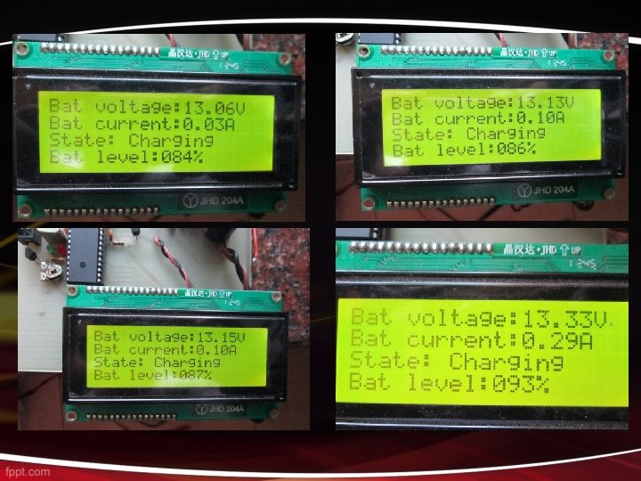
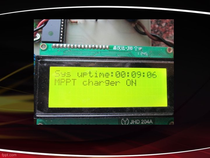
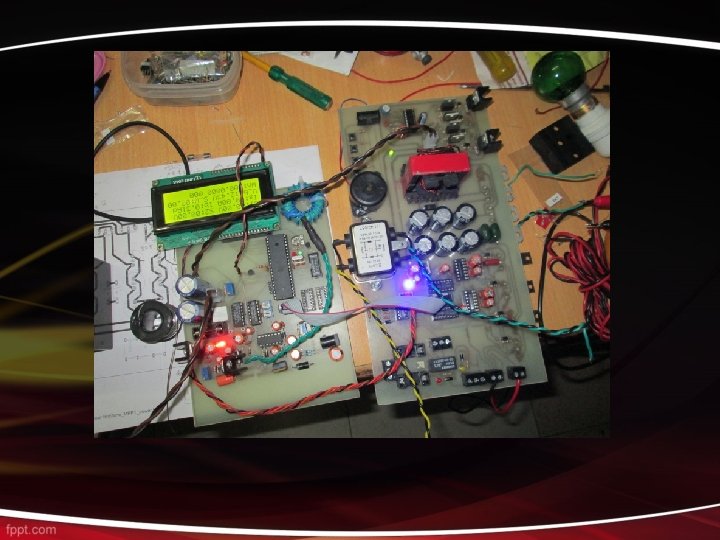
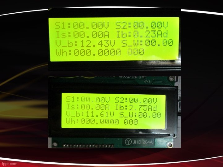
Other necessary circuitry v Battery Charge and discharge current sensing using Hall effect current sensor v Battery voltage monitor v Solar panel voltage & current sense v Mains voltage sense and Zero cross detector v Overload & Short Circuit protection v Change over relay v Auxiliary power supply v LCD Display, Audio alarm , Front panel switches
Mains sense Block diagram Changeover ctrl LCD panel Mains Changeover Relay Filter MOSFET H-Bridge HVDC generation using sg 3525 Supply for gate drive, MCU & other ckts Aux pwr supply Opto coupler Atmega 16 MCU USPWM signals Output sense Gate driver HF transformer & rectifier Switches O/P sense Bat voltage monitor Push Pull converter Battery Charge controller Solar panel Buzzer MPPT control
HF Ferrite Transformer ETD 44 Core used Suitable upto 1 KW power AWG 29 copper wire used to minimize skin effect at high frequency Primary wound using Litz wire to improve current capacity & minimize copper losses
Non overlapping turn on & turn off
Gate Drive signals of High side Mosfets
Component Failures
Further improvements Ø Lead Acid batteries can be replaced with newer lithium iron phosphate (Li. Fe. PO 4) battery. Ø Extremely safe and stable chemistry. Ø Long life-cycle 8 X of Lead acid battery. Ø Light weight with best power-to-weight ratio: 1/3 of Lead acid. Ø Good performance at high temperature Ø Low self-discharge rate, less than 3% monthly. Ø Environment friendly: Clean and Green energy poses no pollution on our environment.
Further improvements Ø Battery elimination possible using ‘Grid-Tie Solar Inverter’ which feeds solar power into the mains grid Ø Better short circuit, overload protection , current sense circuits Ø Enhanced gate drives & IGBT usage Ø Better designed output LC filter Ø Use of a three level PWM signal instead of a two level, this allows a much lower average power output to produce the sine wave needed and assisting in the efficiency of the device
THANK YOU