
Lecture 20 Today we will n Look at

- Slides: 16
Lecture 20 Today we will n Look at why our NMOS and PMOS inverters might not be the best inverter designs n Introduce the CMOS inverter n Analyze how the CMOS inverter works
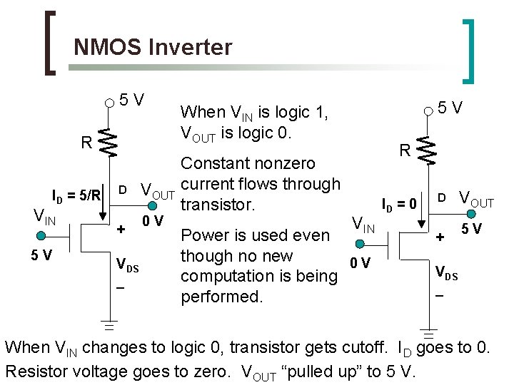
NMOS Inverter 5 V R ID = 5/R VIN 5 V D + VDS _ Constant nonzero VOUT current flows through transistor. 0 V 5 V When VIN is logic 1, VOUT is logic 0. R VIN Power is used even though no new 0 V computation is being performed. ID = 0 D + VOUT 5 V VDS _ When VIN changes to logic 0, transistor gets cutoff. ID goes to 0. Resistor voltage goes to zero. VOUT “pulled up” to 5 V.
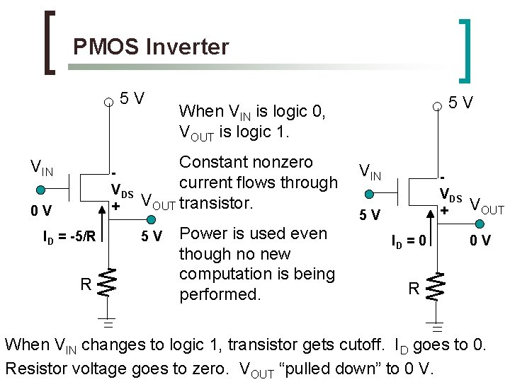
PMOS Inverter 5 V VIN VDS + 0 V ID = -5/R R Constant nonzero current flows through VOUT transistor. 5 V 5 V When VIN is logic 0, VOUT is logic 1. Power is used even though no new computation is being performed. VIN VDS + 5 V ID = 0 VOUT 0 V R When VIN changes to logic 1, transistor gets cutoff. ID goes to 0. Resistor voltage goes to zero. VOUT “pulled down” to 0 V.
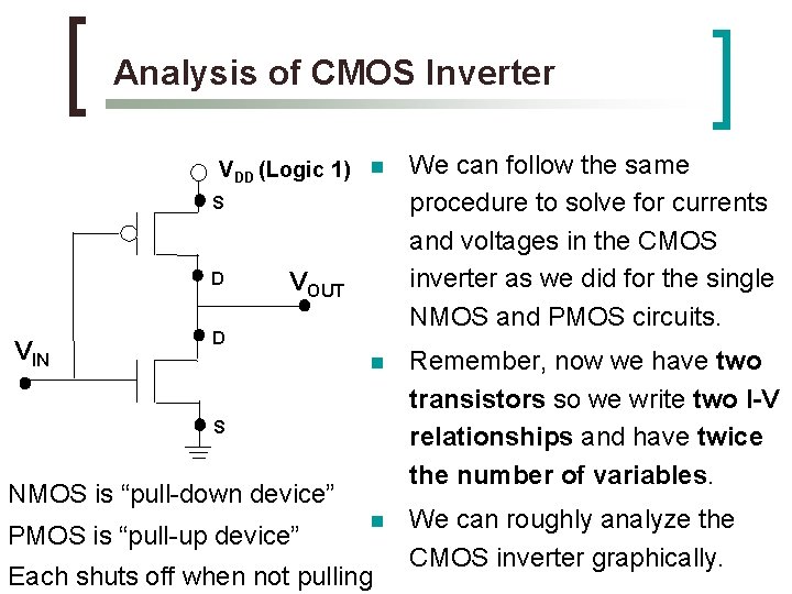
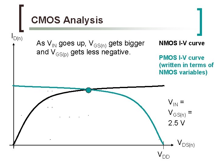
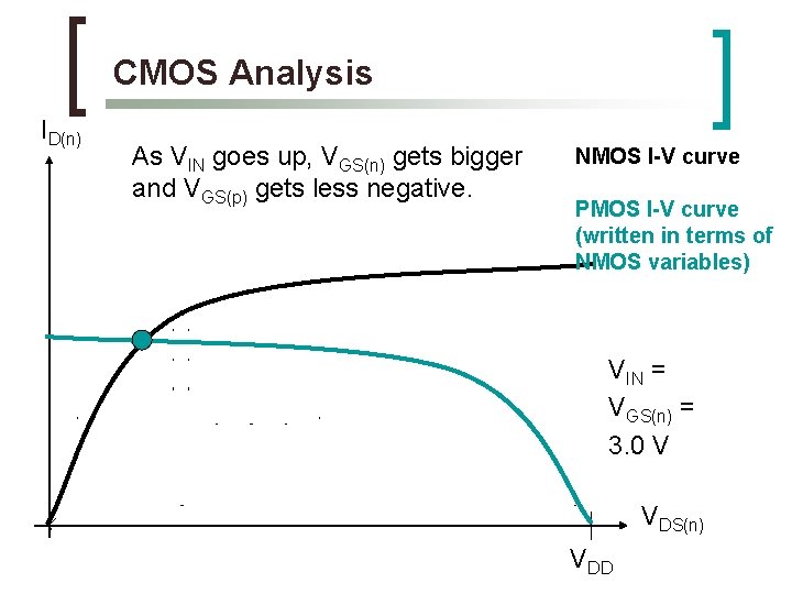
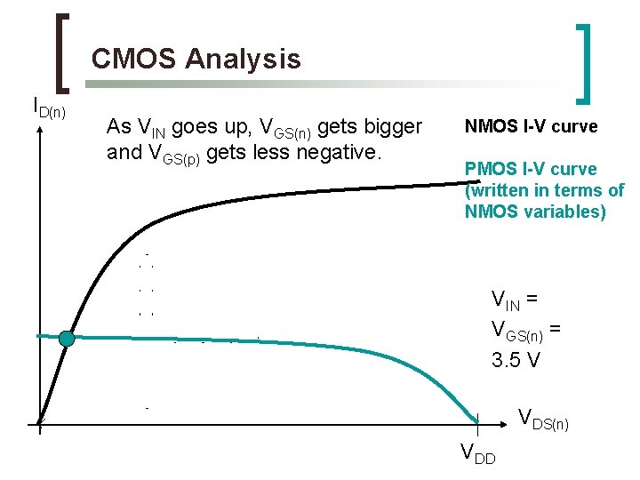
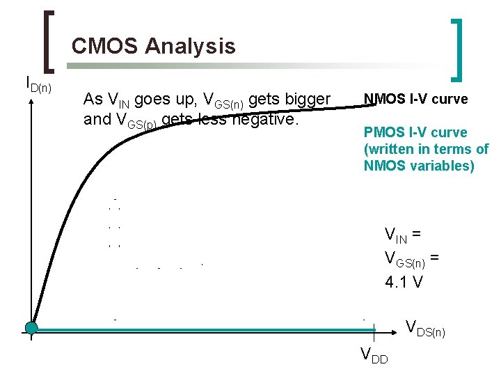
Analysis of CMOS Inverter VDD (Logic 1) n S D VIN VOUT D n Remember, now we have two transistors so we write two I-V relationships and have twice the number of variables. n We can roughly analyze the CMOS inverter graphically. S NMOS is “pull-down device” PMOS is “pull-up device” We can follow the same procedure to solve for currents and voltages in the CMOS inverter as we did for the single NMOS and PMOS circuits. Each shuts off when not pulling
NMOS Inverter ID VGS = 3 V X Linear ID vs VDS given by surrounding circuit X VGS = 1 V VDS
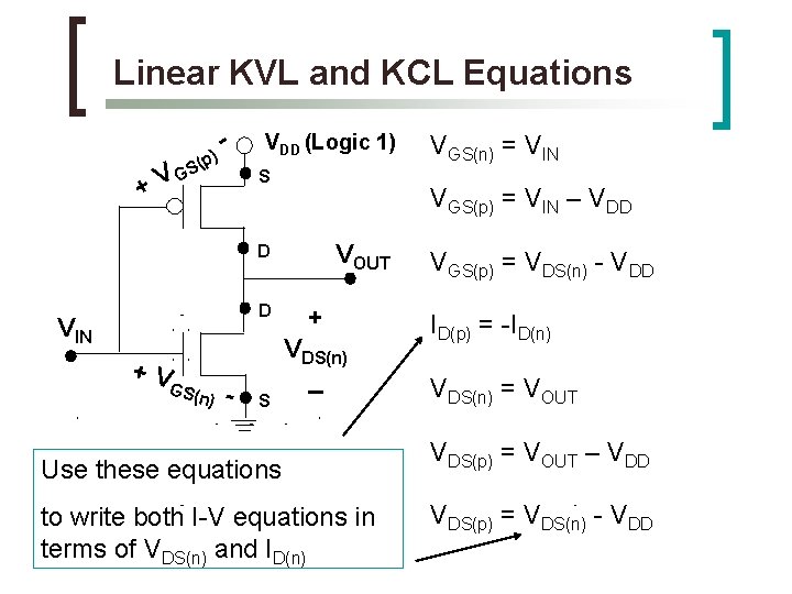
Linear KVL and KCL Equations GS V + (p) - VDD (Logic 1) S VGS(p) = VIN – VDD VOUT D D VIN +V GS(n ) - S VGS(n) = VIN + VDS(n) _ Use these equations to write both I-V equations in terms of VDS(n) and ID(n) VGS(p) = VDS(n) - VDD ID(p) = -ID(n) VDS(n) = VOUT VDS(p) = VOUT – VDD VDS(p) = VDS(n) - VDD
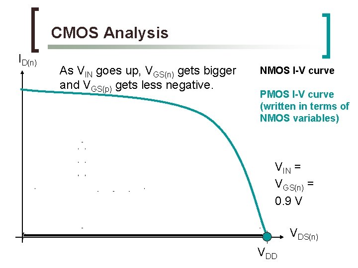
CMOS Analysis ID(n) As VIN goes up, VGS(n) gets bigger and VGS(p) gets less negative. NMOS I-V curve PMOS I-V curve (written in terms of NMOS variables) VIN = VGS(n) = 0. 9 V VDS(n) VDD
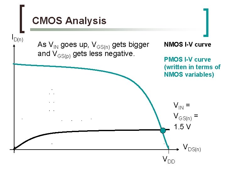
CMOS Analysis ID(n) As VIN goes up, VGS(n) gets bigger and VGS(p) gets less negative. NMOS I-V curve PMOS I-V curve (written in terms of NMOS variables) VIN = VGS(n) = 1. 5 V VDS(n) VDD
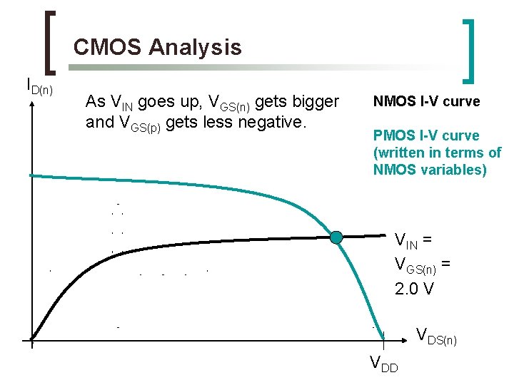
CMOS Analysis ID(n) As VIN goes up, VGS(n) gets bigger and VGS(p) gets less negative. NMOS I-V curve PMOS I-V curve (written in terms of NMOS variables) VIN = VGS(n) = 2. 0 V VDS(n) VDD
CMOS Analysis ID(n) As VIN goes up, VGS(n) gets bigger and VGS(p) gets less negative. NMOS I-V curve PMOS I-V curve (written in terms of NMOS variables) VIN = VGS(n) = 2. 5 V VDS(n) VDD
CMOS Analysis ID(n) As VIN goes up, VGS(n) gets bigger and VGS(p) gets less negative. NMOS I-V curve PMOS I-V curve (written in terms of NMOS variables) VIN = VGS(n) = 3. 0 V VDS(n) VDD
CMOS Analysis ID(n) As VIN goes up, VGS(n) gets bigger and VGS(p) gets less negative. NMOS I-V curve PMOS I-V curve (written in terms of NMOS variables) VIN = VGS(n) = 3. 5 V VDS(n) VDD
CMOS Analysis ID(n) As VIN goes up, VGS(n) gets bigger and VGS(p) gets less negative. NMOS I-V curve PMOS I-V curve (written in terms of NMOS variables) VIN = VGS(n) = 4. 1 V VDS(n) VDD
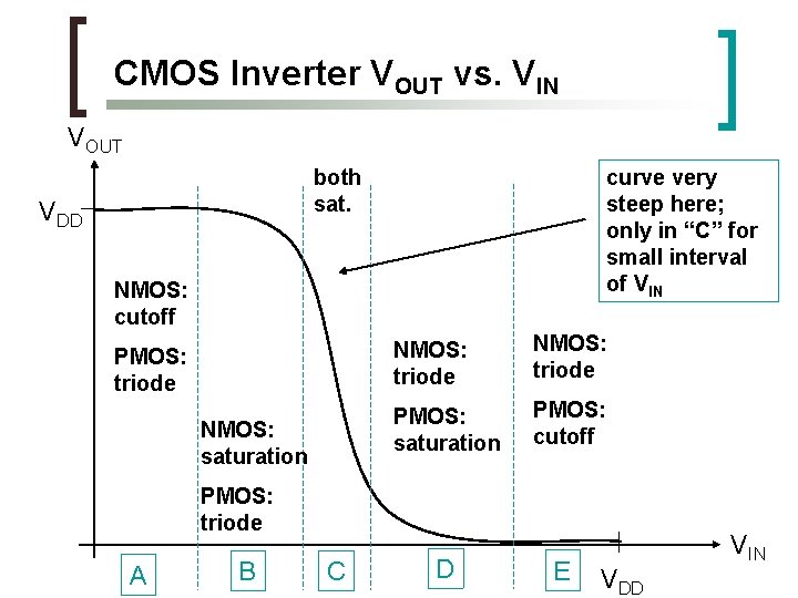
CMOS Inverter VOUT vs. VIN VOUT both sat. VDD curve very steep here; only in “C” for small interval of VIN NMOS: cutoff PMOS: triode NMOS: saturation NMOS: triode PMOS: saturation PMOS: cutoff PMOS: triode A B C D E VIN VDD
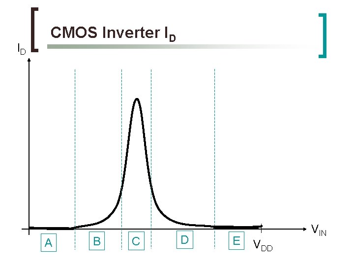
ID CMOS Inverter ID A B C D E VIN VDD
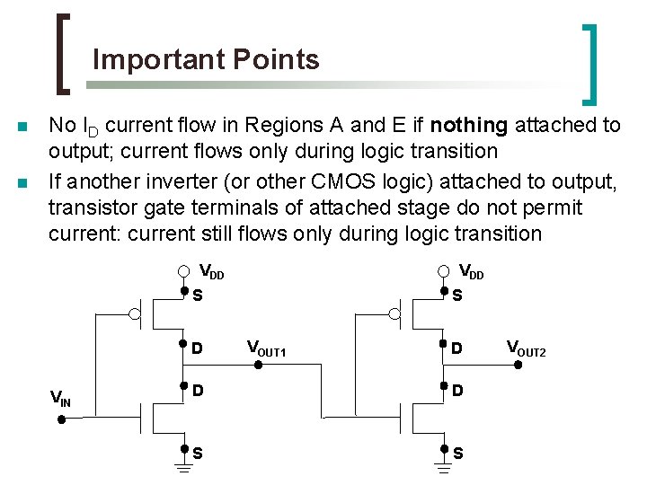
Important Points n n No ID current flow in Regions A and E if nothing attached to output; current flows only during logic transition If another inverter (or other CMOS logic) attached to output, transistor gate terminals of attached stage do not permit current: current still flows only during logic transition VDD S D VIN S VOUT 1 D D D S S VOUT 2