ECE 424 Introduction to VLSI Emre Yengel Department


- Slides: 24

ECE 424 – Introduction to VLSI Emre Yengel Department of Electrical and Communication Engineering Fall 2014

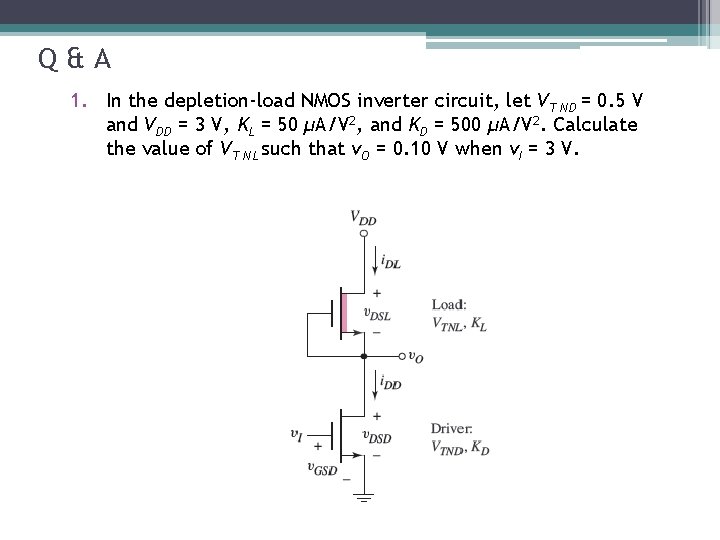
Q&A 1. In the depletion-load NMOS inverter circuit, let VT ND = 0. 5 V and VDD = 3 V, KL = 50 μA/V 2, and KD = 500 μA/V 2. Calculate the value of VT NL such that v. O = 0. 10 V when v. I = 3 V.

Q&A 2. Consider the NMOS inverter with depletion load in Figure 16. 7(a). Let VDD = 1. 8 V, and assume VT ND = 0. 3 V and VT NL = − 0. 6 V. (a) Design the circuit such that the power dissipation is 80μW and the output voltage is v. O = 0. 06 V when v. I is a logic 1. (b) Using the results of part (a), determine the transition points for the driver and load transistors. (c) If (W/L)D found in part (a) is doubled, what is the maximum power dissipation in the inverter and what is v. O when v. I is a logic 1?

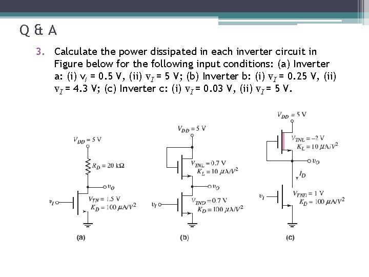
Q&A 3. Calculate the power dissipated in each inverter circuit in Figure below for the following input conditions: (a) Inverter a: (i) v. I = 0. 5 V, (ii) v. I = 5 V; (b) Inverter b: (i) v. I = 0. 25 V, (ii) v. I = 4. 3 V; (c) Inverter c: (i) v. I = 0. 03 V, (ii) v. I = 5 V.

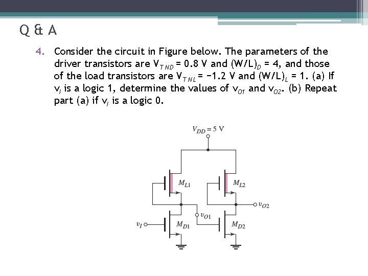
Q&A 4. Consider the circuit in Figure below. The parameters of the driver transistors are VT ND = 0. 8 V and (W/L)D = 4, and those of the load transistors are VT NL = − 1. 2 V and (W/L)L = 1. (a) If v. I is a logic 1, determine the values of v. O 1 and v. O 2. (b) Repeat part (a) if v. I is a logic 0.

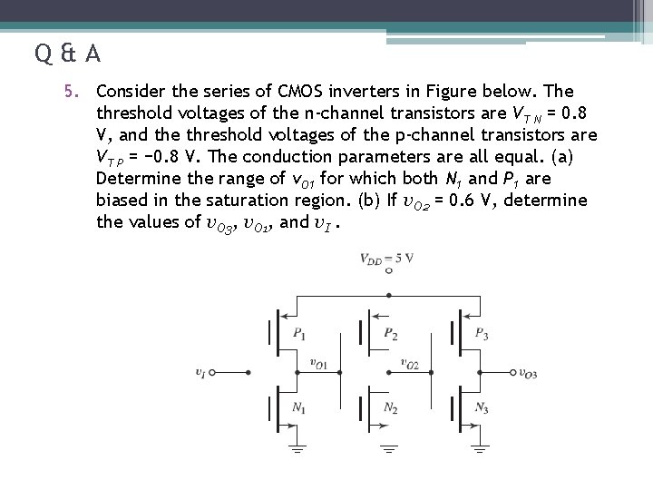
Q&A 5. Consider the series of CMOS inverters in Figure below. The threshold voltages of the n-channel transistors are VT N = 0. 8 V, and the threshold voltages of the p-channel transistors are VT P = − 0. 8 V. The conduction parameters are all equal. (a) Determine the range of v. O 1 for which both N 1 and P 1 are biased in the saturation region. (b) If v. O 2 = 0. 6 V, determine the values of v. O 3, v. O 1, and v. I.

Q&A 6. (a) A CMOS inverter is biased at VDD = 2. 5 V. The transistor parameters are Kn = Kp = 120μA/V 2, VT N = 0. 4 V, and VT P = − 0. 4 V. Calculate the current in the transistors as a function of the input voltage for 0 ≤ v. I ≤ 2. 5 V. (b) Repeat part (a) for VDD = 1. 8 V and 0 ≤ v. I ≤ 1. 8 V.

Q&A 7. A CMOS inverter is biased at VDD = 3. 3 V. The transistor threshold voltages are VT N = +0. 4 V and VT P = − 0. 4 V. Determine the peak current in the inverter and the input voltage at which it occurs for (a) (W/L)n = 3, (W/L)p = 7. 5; (b) (W/L)n = (W/L)p = 4; (c) (W/L)n = 3, (W/L)p = 12. (k’n = 50 and k’p =20)

Q&A 8. (a) A CMOS digital logic circuit contains the equivalent of 4 million CMOS inverters and is biased at VDD = 1. 8 V. The equivalent load capacitance of each inverter is 0. 12 p. F and each inverter is switching at 150 MHz. Determine the total average power dissipated in the circuit. (b) If the switching frequency is doubled, but the total power dissipation is to remain the same with the same load capacitance, determine the required bias voltage.

Q&A 9. A particular IC chip can dissipate 3 W and contains 10 million CMOS inverters. Each inverter is being switched at a frequency f. (a) Determine the average power that each inverter can dissipate without exceeding the total allowed power. (b) If the switching frequency is f = 5 MHz, what is the maximum capacitive load on each inverter if (i) VDD = 5 V, (ii) VDD = 3. 3 V, and (iii) VDD = 1. 5 V.

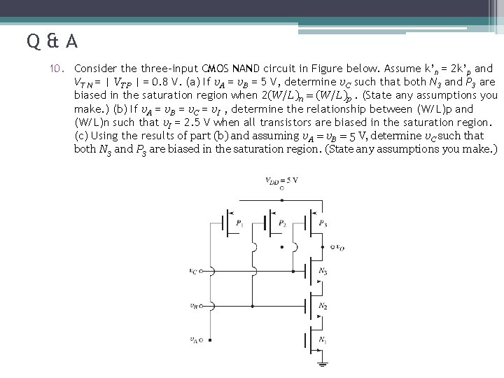
Q&A 10. Consider the three-input CMOS NAND circuit in Figure below. Assume k’n = 2 k’p and VT N = | VT P | = 0. 8 V. (a) If v. A = v. B = 5 V, determine v. C such that both N 3 and P 3 are biased in the saturation region when 2(W/L)n = (W/L)p. (State any assumptions you make. ) (b) If v. A = v. B = v. C = v. I , determine the relationship between (W/L)p and (W/L)n such that v. I = 2. 5 V when all transistors are biased in the saturation region. (c) Using the results of part (b) and assuming v. A = v. B = 5 V, determine v. C such that both N 3 and P 3 are biased in the saturation region. (State any assumptions you make. )

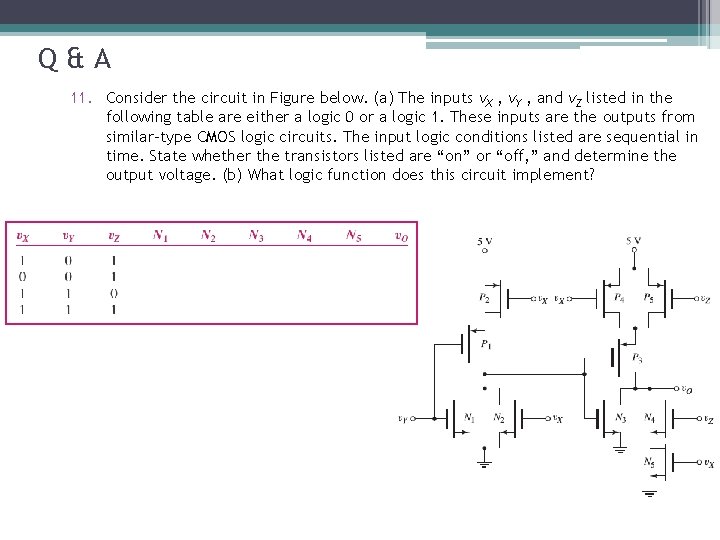
Q&A 11. Consider the circuit in Figure below. (a) The inputs v. X , v. Y , and v. Z listed in the following table are either a logic 0 or a logic 1. These inputs are the outputs from similar-type CMOS logic circuits. The input logic conditions listed are sequential in time. State whether the transistors listed are “on” or “off, ” and determine the output voltage. (b) What logic function does this circuit implement?

Q&A 12. Consider a four-input CMOS NOR logic gate. Determine the W/L ratios of the transistors to provide for symmetrical switching based on the CMOS inverter design with (W/L)n= 2 and (W/L)p= 4. (b) If the load capacitance of the NOR gate doubles, determine the required W/L ratios to provide the same switching speed as the logic gate in part (a).

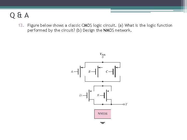
Q&A 13. Figure below shows a classic CMOS logic circuit. (a) What is the logic function performed by the circuit? (b) Design the NMOS network.

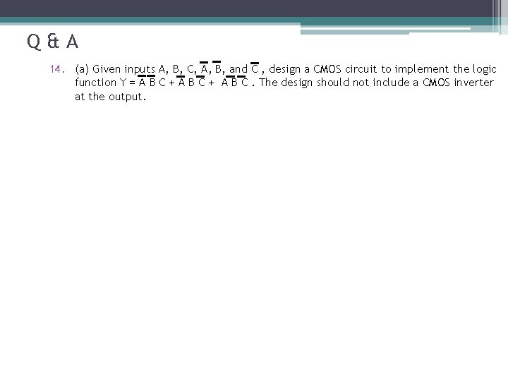
Q&A 14. (a) Given inputs A, B, C, A, B, and C , design a CMOS circuit to implement the logic function Y = A B C + A B C. The design should not include a CMOS inverter at the output.

Q&A 14. (a) Given inputs A, B, C, A, B, and C , design a CMOS circuit to implement the logic function Y = A B C + A B C. The design should not include a CMOS inverter at the output.

Q&A 14. (a) Given inputs A, B, C, A, B, and C , design a CMOS circuit to implement the logic function Y = A B C + A B C. The design should not include a CMOS inverter at the output.

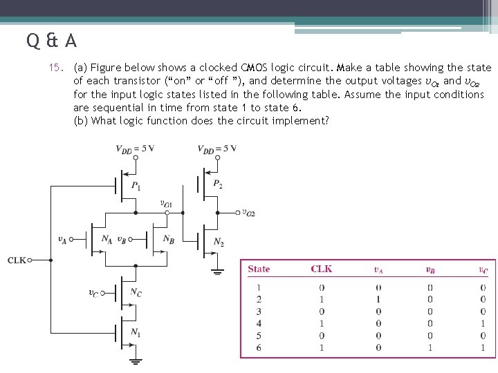
Q&A 15. (a) Figure below shows a clocked CMOS logic circuit. Make a table showing the state of each transistor (“on” or “off ”), and determine the output voltages v. O 1 and v. O 2 for the input logic states listed in the following table. Assume the input conditions are sequential in time from state 1 to state 6. (b) What logic function does the circuit implement?

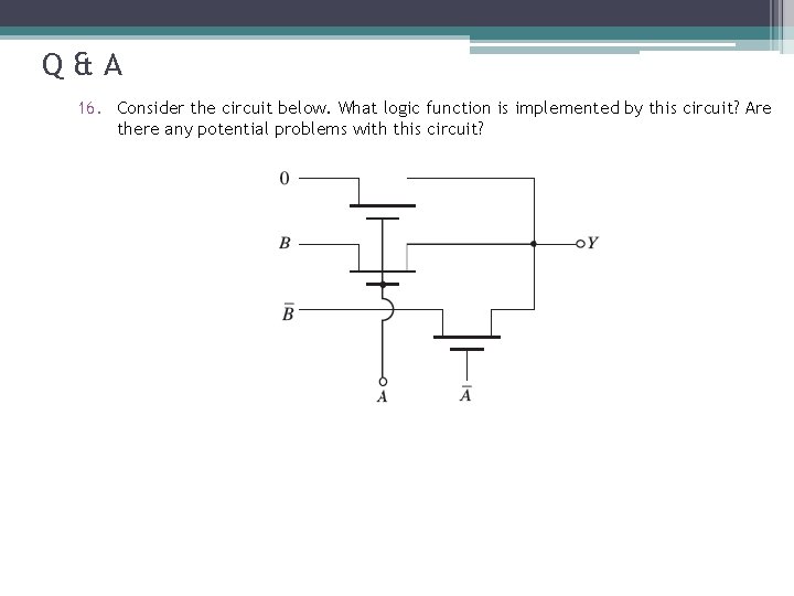
Q&A 16. Consider the circuit below. What logic function is implemented by this circuit? Are there any potential problems with this circuit?

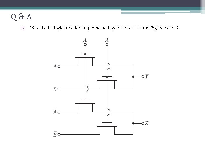
Q&A 17. What is the logic function implemented by the circuit in the Figure below?

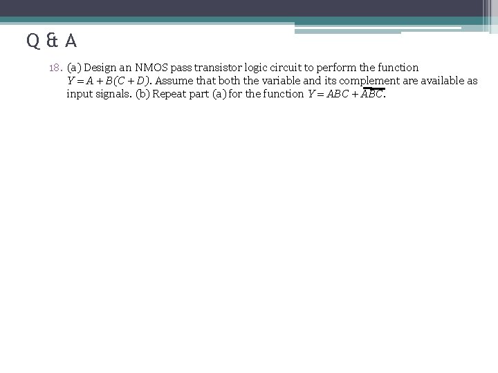
Q&A 18. (a) Design an NMOS pass transistor logic circuit to perform the function Y = A + B(C + D). Assume that both the variable and its complement are available as input signals. (b) Repeat part (a) for the function Y = ABC + ABC.

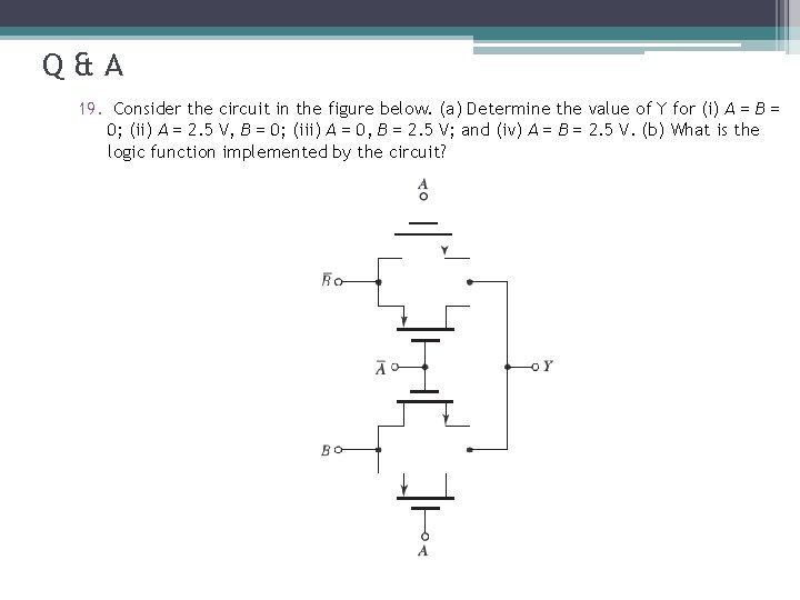
Q&A 19. Consider the circuit in the figure below. (a) Determine the value of Y for (i) A = B = 0; (ii) A = 2. 5 V, B = 0; (iii) A = 0, B = 2. 5 V; and (iv) A = B = 2. 5 V. (b) What is the logic function implemented by the circuit?

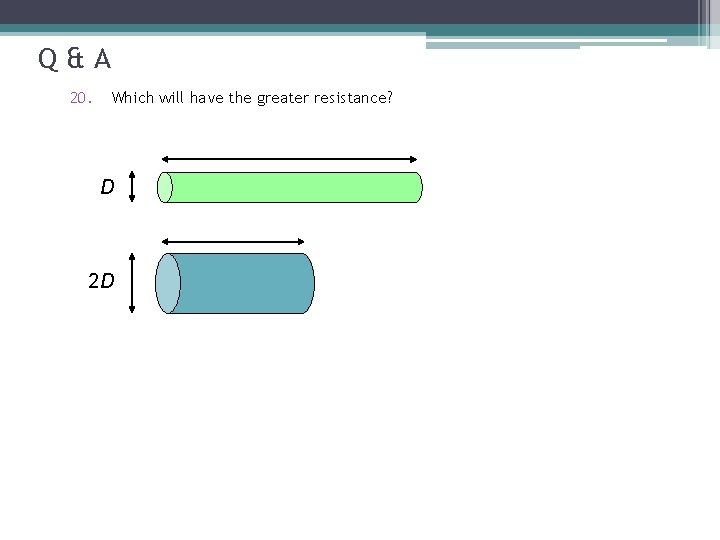
Q&A 20. Which will have the greater resistance? D 2 D

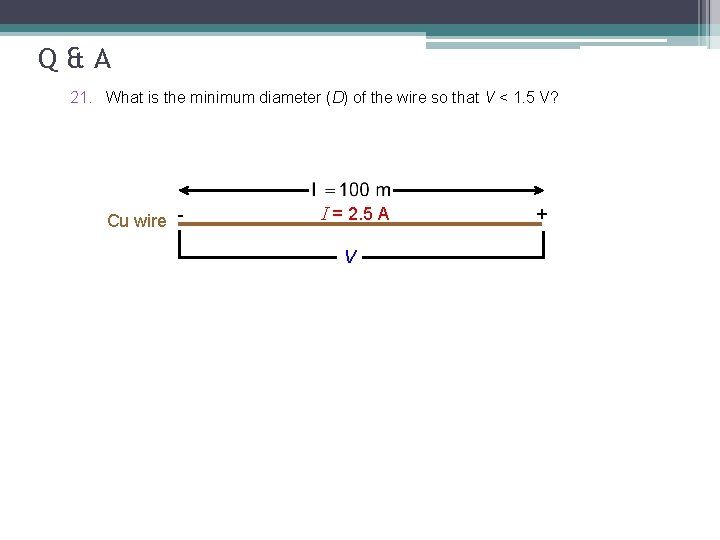
Q&A 21. What is the minimum diameter (D) of the wire so that V < 1. 5 V? Cu wire - I = 2. 5 A V +