ECE 424 Introduction to VLSI Design Emre Yengel

- Slides: 23

ECE 424 – Introduction to VLSI Design Emre Yengel Department of Electrical and Communication Engineering Fall 2014

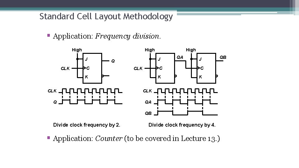
Standard Cell Layout Methodology § Application: Frequency division. High J CLK J Q C High CLK K CLK Q QA QA J C C K K QB QB Divide clock frequency by 2. Divide clock frequency by 4. § Application: Counter (to be covered in Lecture 13. )

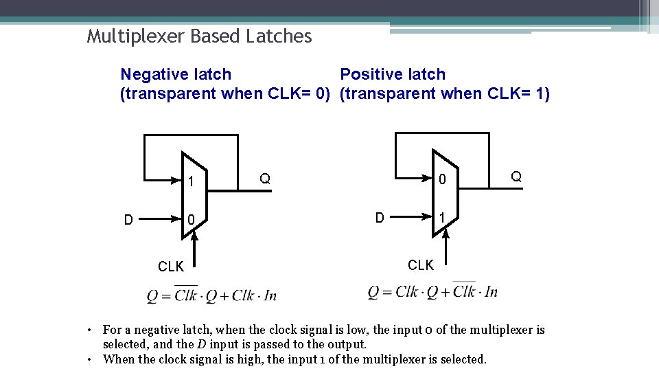
Multiplexer Based Latches Negative latch Positive latch (transparent when CLK= 0) (transparent when CLK= 1) 1 0 D CLK Q 0 Q 1 D CLK • For a negative latch, when the clock signal is low, the input 0 of the multiplexer is selected, and the D input is passed to the output. • When the clock signal is high, the input 1 of the multiplexer is selected.

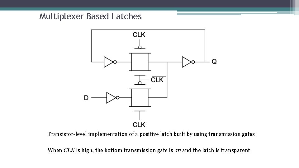
Multiplexer Based Latches Transistor-level implementation of a positive latch built by using transmission gates When CLK is high, the bottom transmission gate is on and the latch is transparent

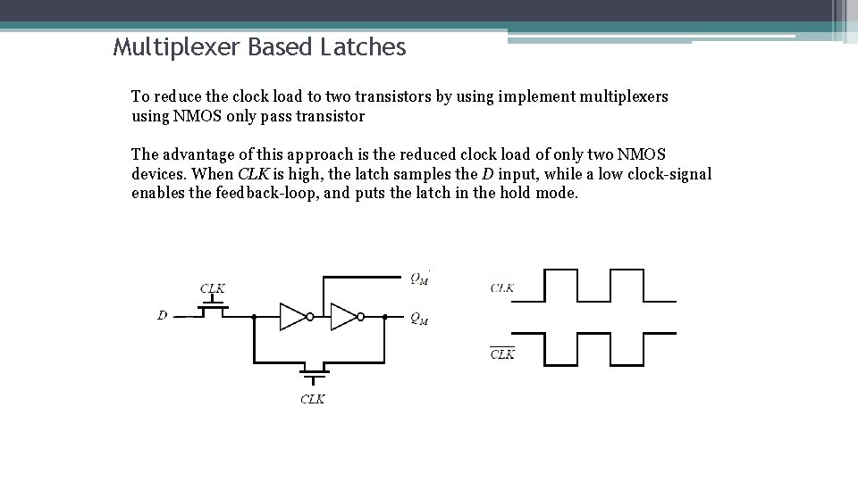
Multiplexer Based Latches To reduce the clock load to two transistors by using implement multiplexers using NMOS only pass transistor The advantage of this approach is the reduced clock load of only two NMOS devices. When CLK is high, the latch samples the D input, while a low clock-signal enables the feedback-loop, and puts the latch in the hold mode.

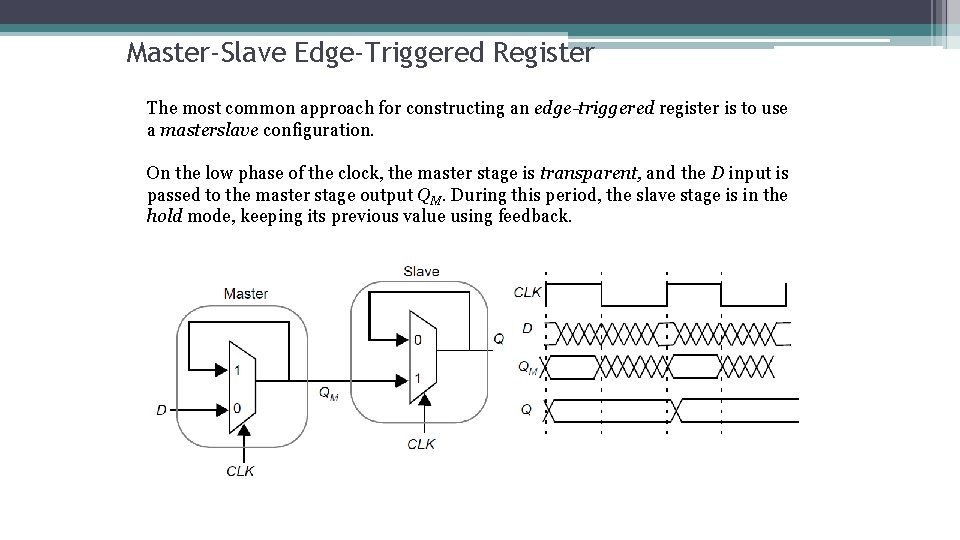
Master-Slave Edge-Triggered Register The most common approach for constructing an edge-triggered register is to use a masterslave configuration. On the low phase of the clock, the master stage is transparent, and the D input is passed to the master stage output QM. During this period, the slave stage is in the hold mode, keeping its previous value using feedback.

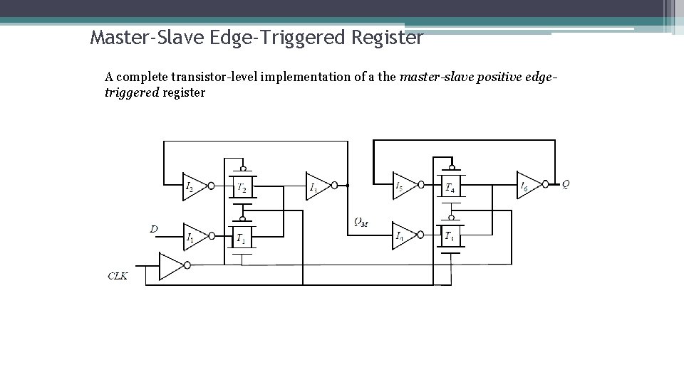
Master-Slave Edge-Triggered Register A complete transistor-level implementation of a the master-slave positive edgetriggered register

Dynamic Latches and Registers • A stored value in a static sequential circuit remains valid as long as the supply voltage is applied to the circuit, hence the name static. • The major disadvantage of the static gate is its complexity. • When registers are used in computational structures , the requirement that the memory should hold state for extended periods of time can be significantly relaxed. This is based on temporary storage of charge on parasitic capacitors. • In this idea, the absence of charge denotes a 0, while its presence stands for a stored 1. A stored value can hence only be kept for a limited amount of time, typically in the range of milliseconds. • If one wants to preserve signal integrity, a periodic refresh of its value is necessary. Hence the name dynamic storage.

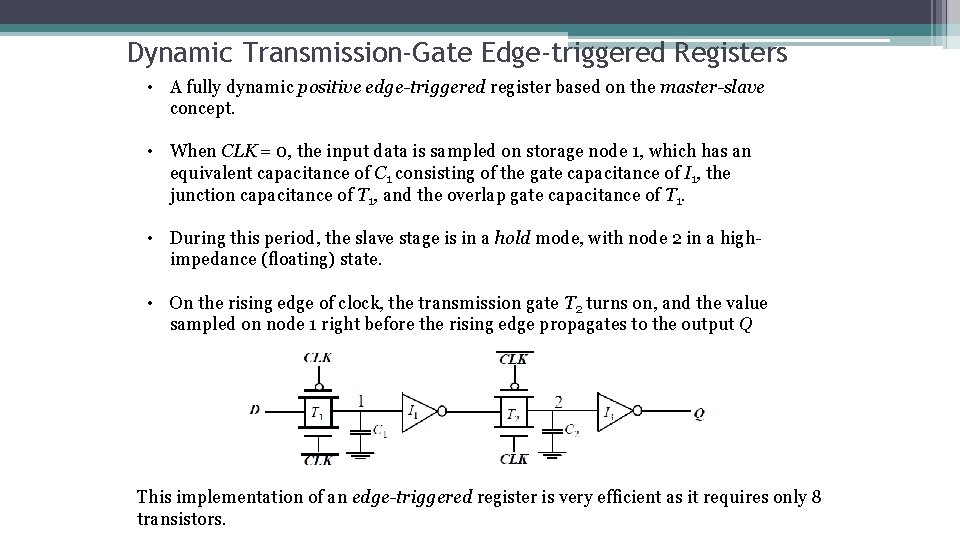
Dynamic Transmission-Gate Edge-triggered Registers • A fully dynamic positive edge-triggered register based on the master-slave concept. • When CLK = 0, the input data is sampled on storage node 1, which has an equivalent capacitance of C 1 consisting of the gate capacitance of I 1, the junction capacitance of T 1, and the overlap gate capacitance of T 1. • During this period, the slave stage is in a hold mode, with node 2 in a highimpedance (floating) state. • On the rising edge of clock, the transmission gate T 2 turns on, and the value sampled on node 1 right before the rising edge propagates to the output Q This implementation of an edge-triggered register is very efficient as it requires only 8 transistors.

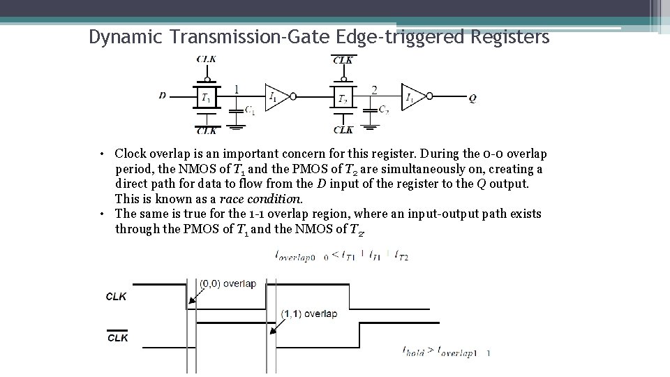
Dynamic Transmission-Gate Edge-triggered Registers • Clock overlap is an important concern for this register. During the 0 -0 overlap period, the NMOS of T 1 and the PMOS of T 2 are simultaneously on, creating a direct path for data to flow from the D input of the register to the Q output. This is known as a race condition. • The same is true for the 1 -1 overlap region, where an input-output path exists through the PMOS of T 1 and the NMOS of T 2.

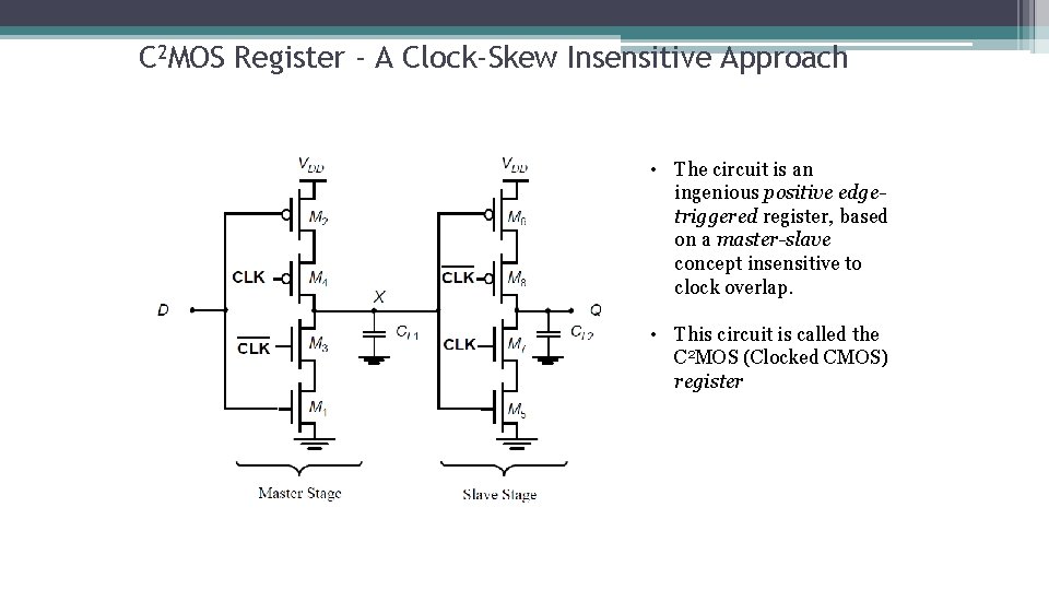
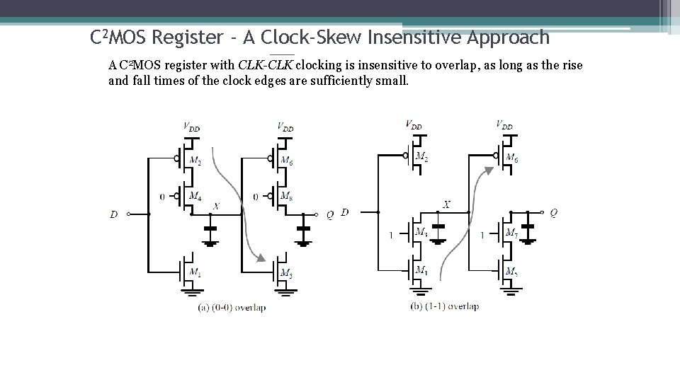
C 2 MOS Register - A Clock-Skew Insensitive Approach • The circuit is an ingenious positive edgetriggered register, based on a master-slave concept insensitive to clock overlap. • This circuit is called the C 2 MOS (Clocked CMOS) register

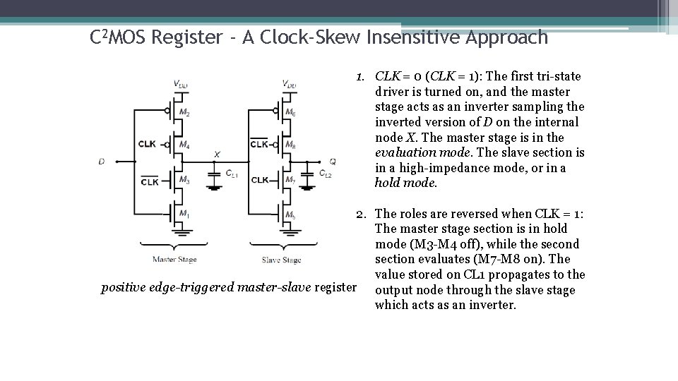
C 2 MOS Register - A Clock-Skew Insensitive Approach 1. CLK = 0 (CLK = 1): The first tri-state driver is turned on, and the master stage acts as an inverter sampling the inverted version of D on the internal node X. The master stage is in the evaluation mode. The slave section is in a high-impedance mode, or in a hold mode. 2. The roles are reversed when CLK = 1: The master stage section is in hold mode (M 3 -M 4 off), while the second section evaluates (M 7 -M 8 on). The value stored on CL 1 propagates to the positive edge-triggered master-slave register output node through the slave stage which acts as an inverter.

C 2 MOS Register - A Clock-Skew Insensitive Approach A C 2 MOS register with CLK-CLK clocking is insensitive to overlap, as long as the rise and fall times of the clock edges are sufficiently small.

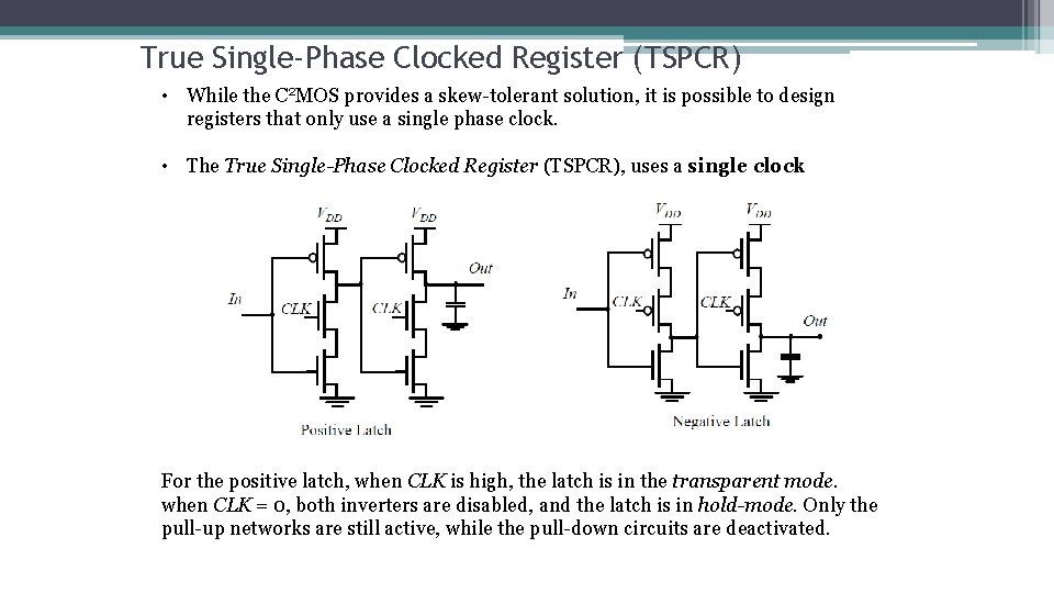
True Single-Phase Clocked Register (TSPCR) • While the C 2 MOS provides a skew-tolerant solution, it is possible to design registers that only use a single phase clock. • The True Single-Phase Clocked Register (TSPCR), uses a single clock For the positive latch, when CLK is high, the latch is in the transparent mode. when CLK = 0, both inverters are disabled, and the latch is in hold-mode. Only the pull-up networks are still active, while the pull-down circuits are deactivated.

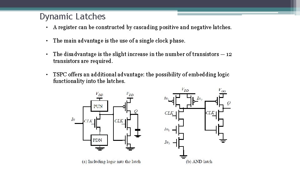
Dynamic Latches • A register can be constructed by cascading positive and negative latches. • The main advantage is the use of a single clock phase. • The disadvantage is the slight increase in the number of transistors — 12 transistors are required. • TSPC offers an additional advantage: the possibility of embedding logic functionality into the latches.

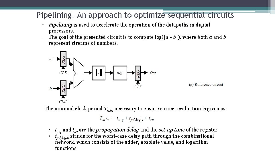
Pipelining: An approach to optimize sequential circuits • Pipelining is used to accelerate the operation of the datapaths in digital processors. • The goal of the presented circuit is to compute log(|a - b|), where both a and b represent streams of numbers. The minimal clock period Tmin necessary to ensure correct evaluation is given as: • tc-q and tsu are the propagation delay and the set-up time of the register • tpd, logic stands for the worst-case delay path through the combinational network, which consists of the adder, absolute value, and logarithm functions.

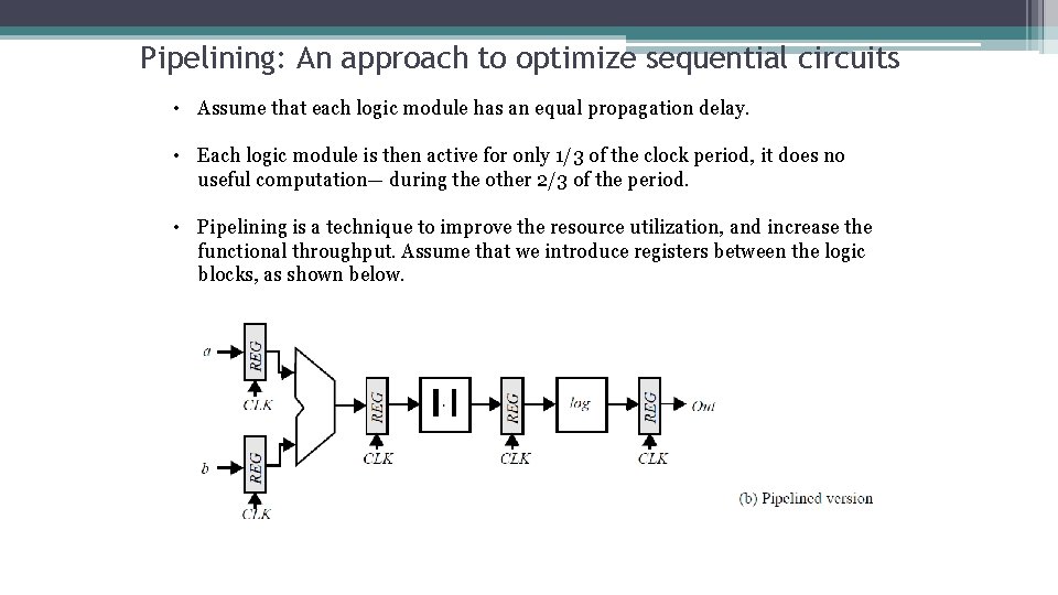
Pipelining: An approach to optimize sequential circuits • Assume that each logic module has an equal propagation delay. • Each logic module is then active for only 1/3 of the clock period, it does no useful computation— during the other 2/3 of the period. • Pipelining is a technique to improve the resource utilization, and increase the functional throughput. Assume that we introduce registers between the logic blocks, as shown below.

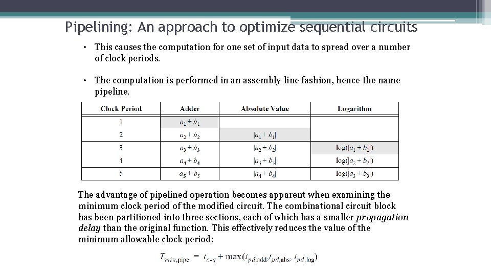
Pipelining: An approach to optimize sequential circuits • This causes the computation for one set of input data to spread over a number of clock periods. • The computation is performed in an assembly-line fashion, hence the name pipeline. The advantage of pipelined operation becomes apparent when examining the minimum clock period of the modified circuit. The combinational circuit block has been partitioned into three sections, each of which has a smaller propagation delay than the original function. This effectively reduces the value of the minimum allowable clock period:

Non-Bistable Sequential Circuits • The most important property of a latch circuit is that it has two stable states, and is hence called bistable. • Other regenerative circuits can be catalogued as astable and monostable. • Another interesting regenerative circuit is the Schmitt trigger: its switching threshold is variable and depends upon the direction of the transition (low-tohigh or high-to-low). This peculiar feature can come in handy in noisy environments.

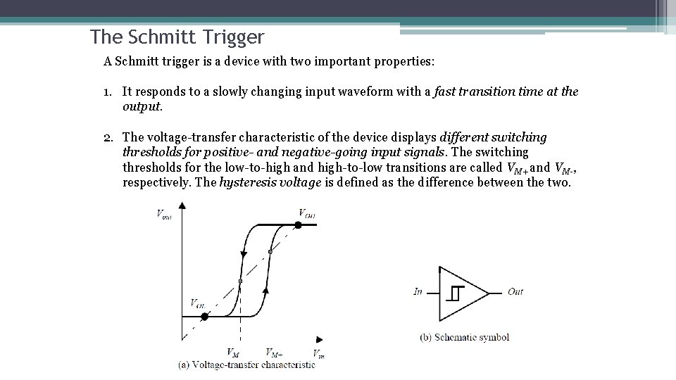
The Schmitt Trigger A Schmitt trigger is a device with two important properties: 1. It responds to a slowly changing input waveform with a fast transition time at the output. 2. The voltage-transfer characteristic of the device displays different switching thresholds for positive- and negative-going input signals. The switching thresholds for the low-to-high and high-to-low transitions are called VM+ and VM-, respectively. The hysteresis voltage is defined as the difference between the two.

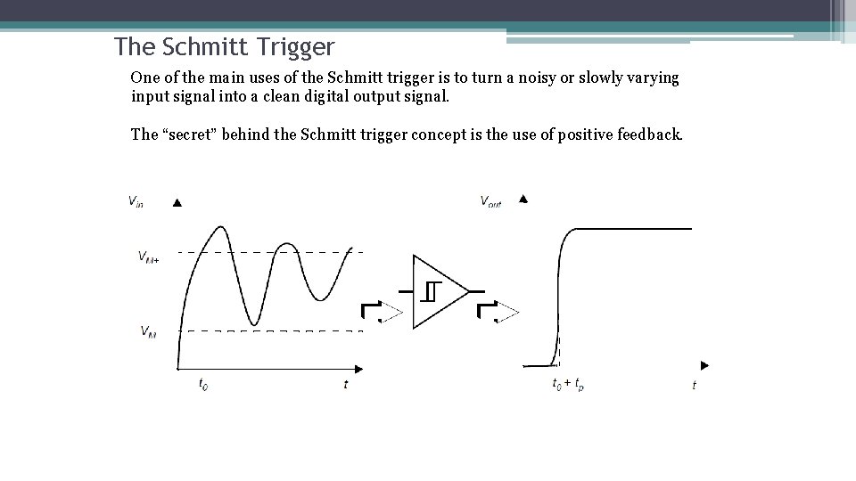
The Schmitt Trigger One of the main uses of the Schmitt trigger is to turn a noisy or slowly varying input signal into a clean digital output signal. The “secret” behind the Schmitt trigger concept is the use of positive feedback.

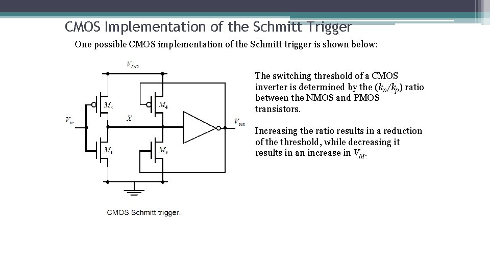
CMOS Implementation of the Schmitt Trigger One possible CMOS implementation of the Schmitt trigger is shown below: The switching threshold of a CMOS inverter is determined by the (kn/kp) ratio between the NMOS and PMOS transistors. Increasing the ratio results in a reduction of the threshold, while decreasing it results in an increase in VM.

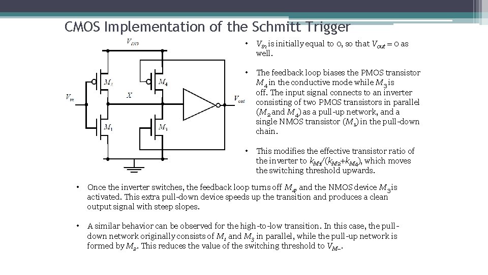
CMOS Implementation of the Schmitt Trigger • Vin is initially equal to 0, so that Vout = 0 as well. • The feedback loop biases the PMOS transistor M 4 in the conductive mode while M 3 is off. The input signal connects to an inverter consisting of two PMOS transistors in parallel (M 2 and M 4) as a pull-up network, and a single NMOS transistor (M 1) in the pull-down chain. • This modifies the effective transistor ratio of the inverter to k. M 1/(k. M 2+k. M 4), which moves the switching threshold upwards. • Once the inverter switches, the feedback loop turns off M 4, and the NMOS device M 3 is activated. This extra pull-down device speeds up the transition and produces a clean output signal with steep slopes. • A similar behavior can be observed for the high-to-low transition. In this case, the pulldown network originally consists of M 1 and M 3 in parallel, while the pull-up network is formed by M 2. This reduces the value of the switching threshold to VM–.