ECE 424 Introduction to VLSI Design Emre Yengel

- Slides: 41

ECE 424 – Introduction to VLSI Design Emre Yengel Department of Electrical and Communication Engineering Fall 2014

Goals of This Course • Understand the manufacturing technologies of integrated semiconductor devices and integrated circuits • Learn to design and implement state-of-the-art digital Very Large Scale Integrated (VLSI) chips using CMOS technology • Learn to analyze sequential circuits designed by CMOS technology • Learn to analyze, simulate and test of the digital design by CAD tools (KICAD will be used) • Learn the basics of Xilinx FPGA

Course Information Instructor • Emre Yengel • Office: L 106 • +90 -312 -233 -1309 • e. yengel@cankaya. edu. tr More on Course • Course Web Page: ece 424. cankaya. edu. tr • Text Book: Digital Integrated Circuits (2 nd ed. ), Jan M. Rabaey, 2002 • Lectures in class will cover basics of course • Homeworks will help you gain a deep understanding of the subject • Assessment: HWs (%15), Attendance (%10), Lab (%20), Midterm (%25), Final (%30) • Lab sessions will cover PSPICE and FPGA basics

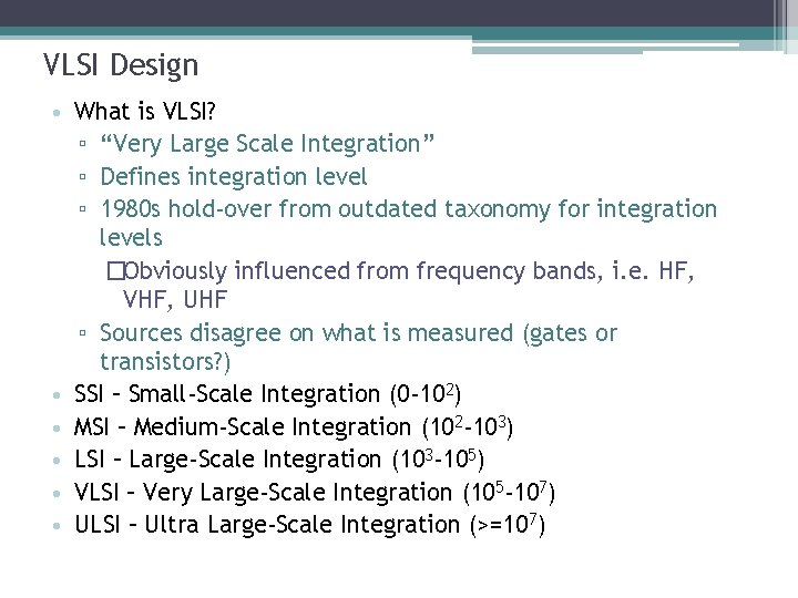
VLSI Design • What is VLSI? ▫ “Very Large Scale Integration” ▫ Defines integration level ▫ 1980 s hold-over from outdated taxonomy for integration levels �Obviously influenced from frequency bands, i. e. HF, VHF, UHF ▫ Sources disagree on what is measured (gates or transistors? ) • SSI – Small-Scale Integration (0 -102) • MSI – Medium-Scale Integration (102 -103) • LSI – Large-Scale Integration (103 -105) • VLSI – Very Large-Scale Integration (105 -107) • ULSI – Ultra Large-Scale Integration (>=107)

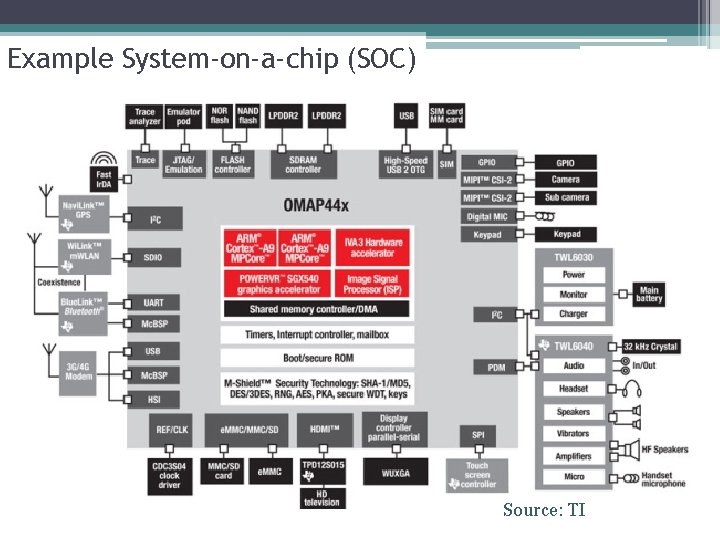
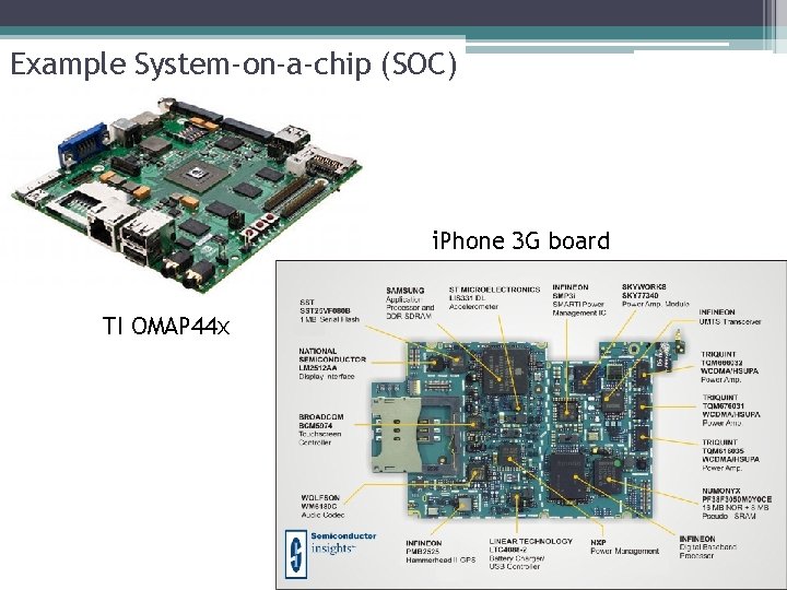
Example System-on-a-chip (SOC) Source: TI

Example System-on-a-chip (SOC) i. Phone 3 G board TI OMAP 44 x

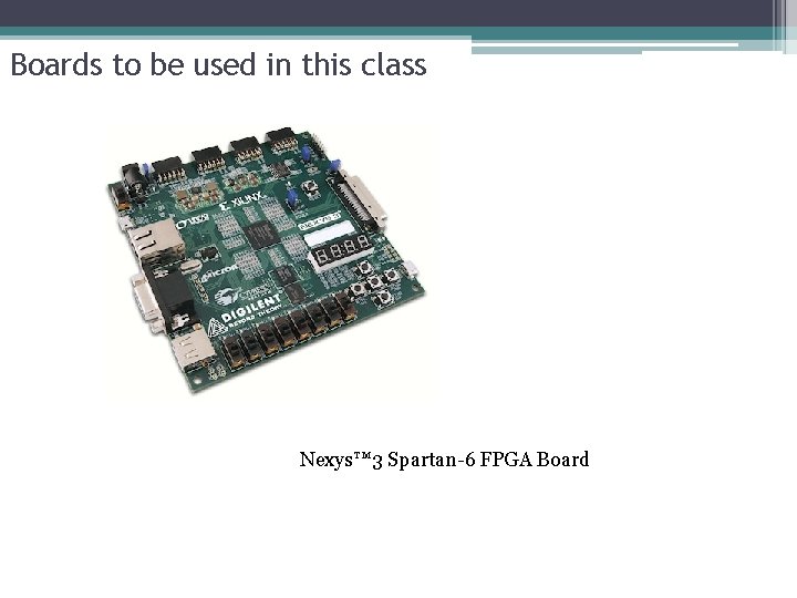
Boards to be used in this class Nexys™ 3 Spartan-6 FPGA Board

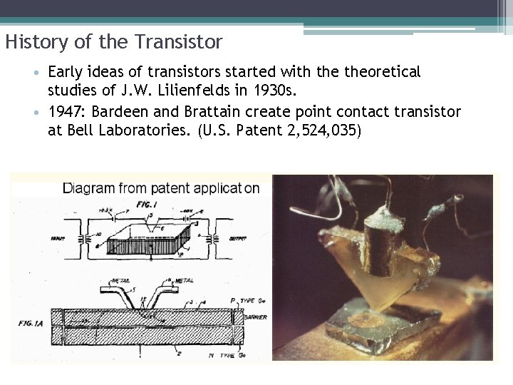
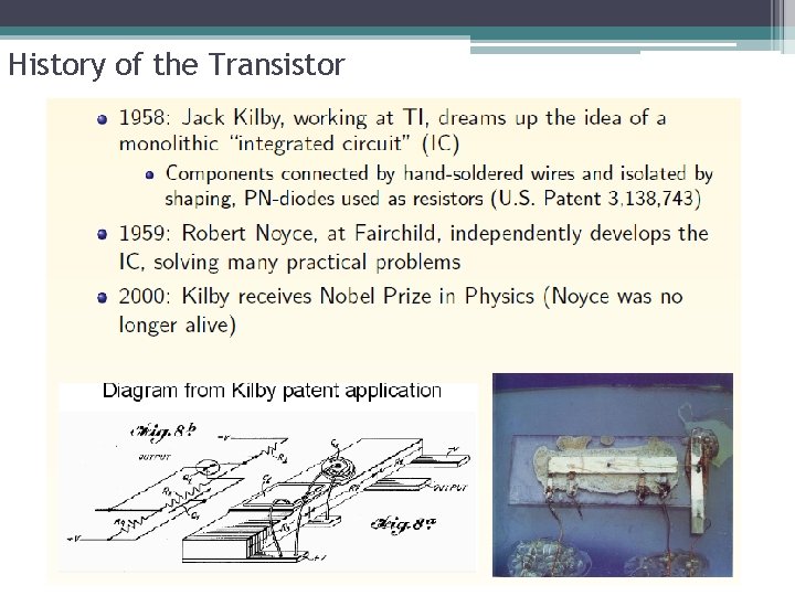
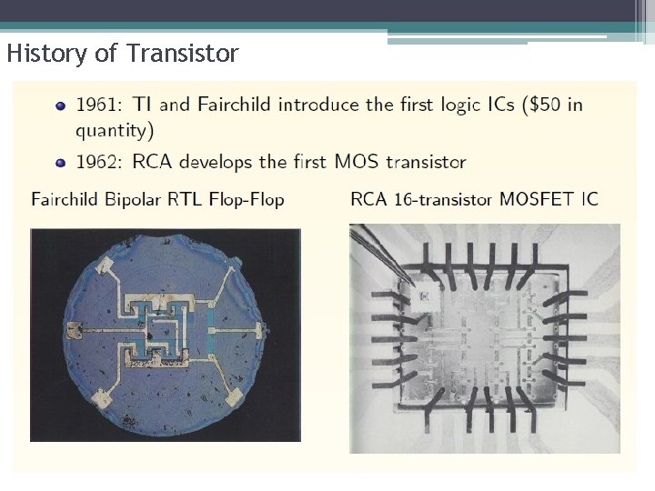
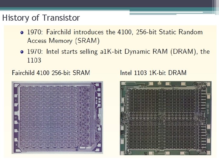
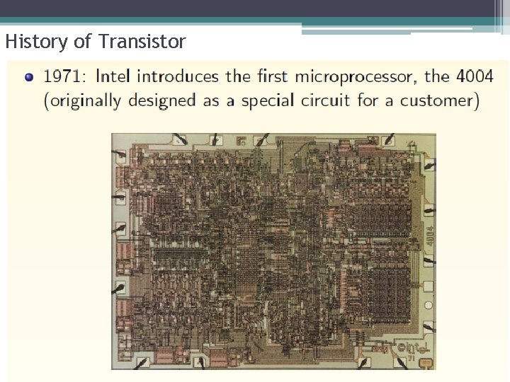
History of the Transistor • Early ideas of transistors started with theoretical studies of J. W. Lilienfelds in 1930 s. • 1947: Bardeen and Brattain create point contact transistor at Bell Laboratories. (U. S. Patent 2, 524, 035)

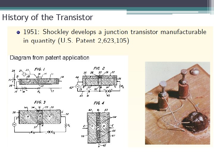
History of the Transistor

History of the Transistor

History of Transistor

History of Transistor

History of Transistor

History of Transistor

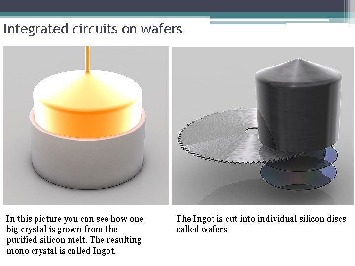
Integrated circuits on wafers In this picture you can see how one big crystal is grown from the purified silicon melt. The resulting mono crystal is called Ingot. The Ingot is cut into individual silicon discs called wafers

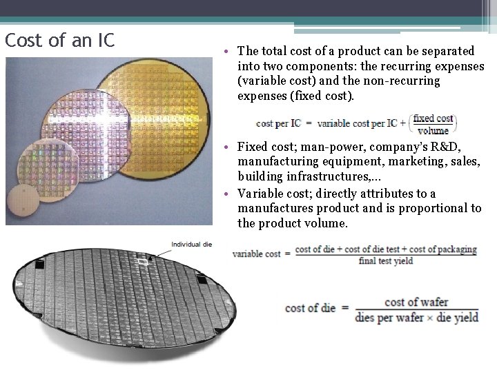
Cost of an IC • The total cost of a product can be separated into two components: the recurring expenses (variable cost) and the non-recurring expenses (fixed cost). • Fixed cost; man-power, company’s R&D, manufacturing equipment, marketing, sales, building infrastructures, … • Variable cost; directly attributes to a manufactures product and is proportional to the product volume.

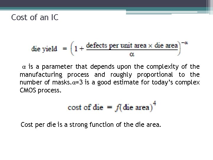
Cost of an IC α is a parameter that depends upon the complexity of the manufacturing process and roughly proportional to the number of masks. α=3 is a good estimate for today’s complex CMOS process. Cost per die is a strong function of the die area.

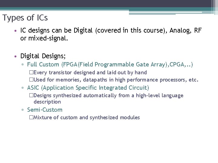
Types of ICs • IC designs can be Digital (covered in this course), Analog, RF or mixed-signal. • Digital Designs; ▫ Full Custom (FPGA(Field Programmable Gate Array), CPGA, . . ) �Every transistor designed and laid out by hand �Used for memories, datapaths in high performance processors, etc. ▫ ASIC (Application Specific Integrated Circuit) �Designs synthesized automatically from a high-level language description ▫ Semi-Custom �Mixture of custom and synthesized modules

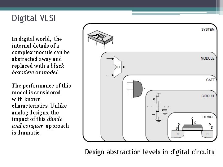
Digital VLSI In digital world, the internal details of a complex module can be abstracted away and replaced with a black box view or model. The performance of this model is considered with known characteristics. Unlike analog designs, the impact of this divide and conquer approach is dramatic. Design abstraction levels in digital circuits

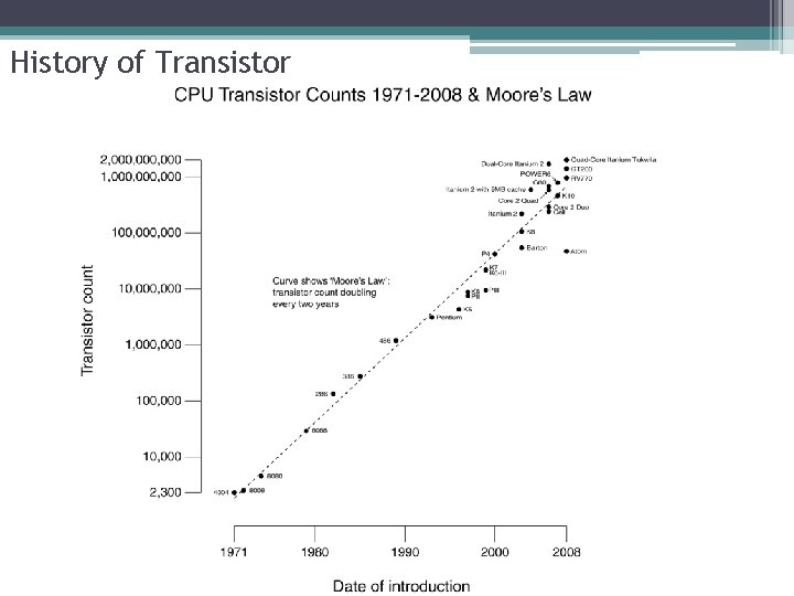
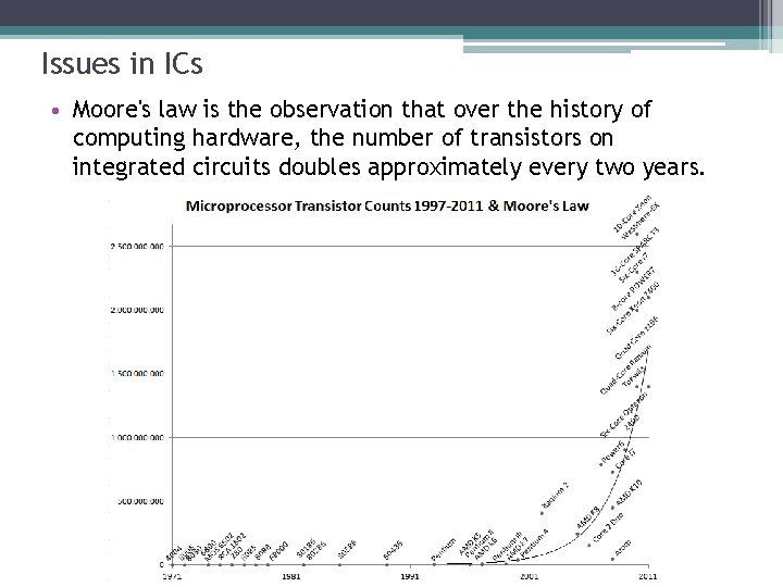
Issues in ICs • Moore's law is the observation that over the history of computing hardware, the number of transistors on integrated circuits doubles approximately every two years.

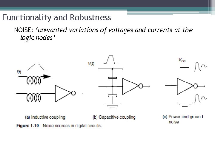
Functionality and Robustness NOISE: ‘unwanted variations of voltages and currents at the logic nodes’

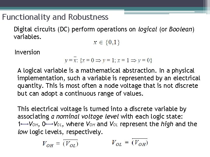
Functionality and Robustness Digital circuits (DC) perform operations on logical (or Boolean) variables. Inversion A logical variable is a mathematical abstraction. In a physical implementation, such a variable is represented by an electrical quantity. This is most often a node voltage that is not discrete but can adopt a continuous range of values. This electrical voltage is turned into a discrete variable by associating a nominal voltage level with each logic state: 1 VOH, 0 VOL, where VOH and VOL represent the high and the low logic levels, respectively.

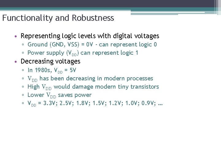
Functionality and Robustness • Representing logic levels with digital voltages ▫ Ground (GND, VSS) = 0 V - can represent logic 0 ▫ Power supply (VDD) can represent logic 1 • Decreasing voltages ▫ ▫ ▫ In 1980 s, VDD = 5 V VDD has been decreasing in modern processes High VDD would damage modern tiny transistors Lower VDD saves power VDD = 3. 3 V; 2. 5 V; 1. 8 V; 1. 5 V; 1. 2 V; 1. 0 V; 0. 9 V; …

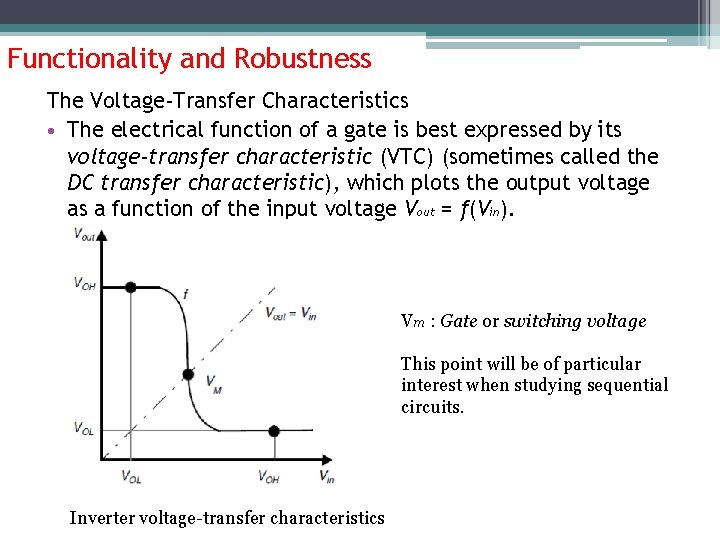
Functionality and Robustness The Voltage-Transfer Characteristics • The electrical function of a gate is best expressed by its voltage-transfer characteristic (VTC) (sometimes called the DC transfer characteristic), which plots the output voltage as a function of the input voltage Vout = f(Vin). Vm : Gate or switching voltage This point will be of particular interest when studying sequential circuits. Inverter voltage-transfer characteristics

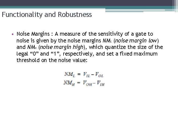
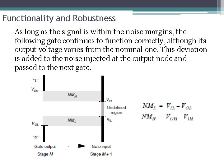
Functionality and Robustness • Noise Margins : A measure of the sensitivity of a gate to noise is given by the noise margins NML (noise margin low) and NMH (noise margin high), which quantize the size of the legal “ 0” and “ 1”, respectively, and set a fixed maximum threshold on the noise value:

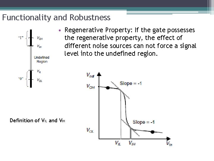
Functionality and Robustness • Regenerative Property: If the gate possesses the regenerative property, the effect of different noise sources can not force a signal level into the undefined region. Definition of VIL and VIH

Functionality and Robustness As long as the signal is within the noise margins, the following gate continues to function correctly, although its output voltage varies from the nominal one. This deviation is added to the noise injected at the output node and passed to the next gate.

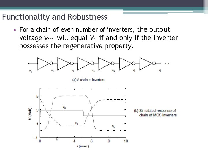
Functionality and Robustness • For a chain of even number of inverters, the output voltage vout will equal VOL if and only if the inverter possesses the regenerative property.

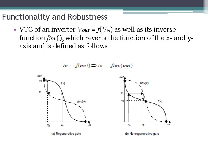
Functionality and Robustness • VTC of an inverter Vout = f(Vin) as well as its inverse function finv(), which reverts the function of the x- and yaxis and is defined as follows:

Functionality and Robustness • Noise Immunity: expresses the ability of the system to process and transmit information correctly in the presence of noise. • A system with good noise immunity must reject the noise instead of overpowering it. • Directivity: a gate to be unidirectional which changes in an output level should not appear at any unchanging input of the same circuit.

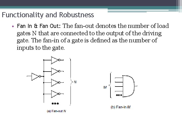
Functionality and Robustness • Fan In & Fan Out: The fan-out denotes the number of load gates N that are connected to the output of the driving gate. The fan-in of a gate is defined as the number of inputs to the gate.

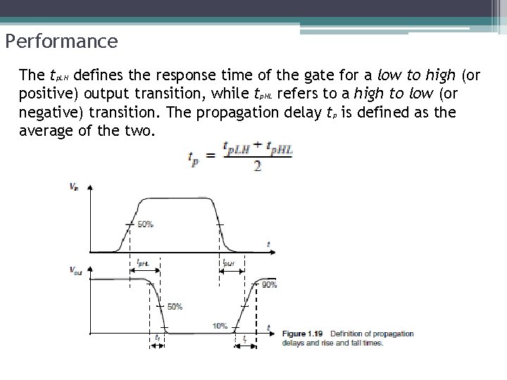
Performance • Performance of a digital circuit can be expressed with the computational ability that the circuit can manage. It is often expressed by the duration of the clock period (clock cycle time), or its rate (clock frequency). • The propagation delay tp of a gate defines how quickly it responds to a change at its input(s). It expresses the delay experienced by a signal when passing through a gate. It is measured between the 50% transition points of the input and output waveforms

Performance The tp. LH defines the response time of the gate for a low to high (or positive) output transition, while tp. HL refers to a high to low (or negative) transition. The propagation delay tp is defined as the average of the two.

Performance • The delay is a function of the slopes of the input and output signals of the gate. To quantify this, the rise and fall times tr and tf, which express how fast a signal transits between the different levels. • The rise/fall time of a signal is largely determined by the strength of the driving gate, and the load presented by the node itself, which sums the contributions of the connecting gates (fan-out) and the wiring parasitics.

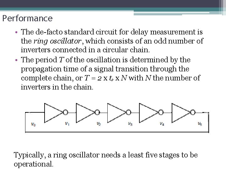
Performance • The de-facto standard circuit for delay measurement is the ring oscillator, which consists of an odd number of inverters connected in a circular chain. • The period T of the oscillation is determined by the propagation time of a signal transition through the complete chain, or T = 2 x tp x N with N the number of inverters in the chain. Typically, a ring oscillator needs a least five stages to be operational.

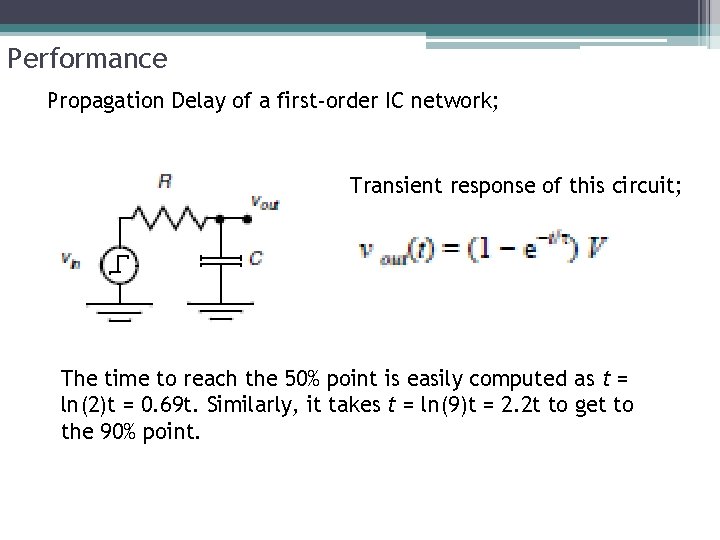
Performance Propagation Delay of a first-order IC network; Transient response of this circuit; The time to reach the 50% point is easily computed as t = ln(2)t = 0. 69 t. Similarly, it takes t = ln(9)t = 2. 2 t to get to the 90% point.

Power and Energy Consumption • The power consumption of a design determines how much energy is consumed per operation, and how much heat the circuit dissipates. • These factors influence a great number of critical design decisions; ▫ ▫ the power-supply capacity the battery lifetime supply-line sizing packaging and cooling requirements • So, power dissipation is an important property of a design that affects feasibility, cost, and reliability.

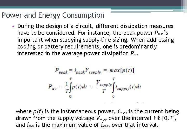
Power and Energy Consumption • During the design of a circuit, different dissipation measures have to be considered. For instance, the peak power Ppeak is important when studying supply-line sizing. When addressing cooling or battery requirements, one is predominantly interested in the average power dissipation Pav. where p(t) is the instantaneous power, isupply is the current being drawn from the supply voltage Vsupply over the interval t € [0, T], and ipeak is the maximum value of isupply over that interval.

Power and Energy Consumption • The dissipation can further be decomposed into static and dynamic components. • The propagation delay and the power consumption of a gate are related—the propagation delay is mostly determined by the speed at which a given amount of energy can be stored on the gate capacitors. • The product of power consumption and propagation delay is generally a constant. This product is called the power-delay product (or PDP) and can be considered as a quality measure for a switching device. The PDP is simply the energy consumed by the gate per switching event.

Power and Energy Consumption • An ideal gate is one that is fast, and consumes little energy. The energy-delay product (E-D) is a combined metric that brings those two elements together, and is often used as the ultimate quality metric.

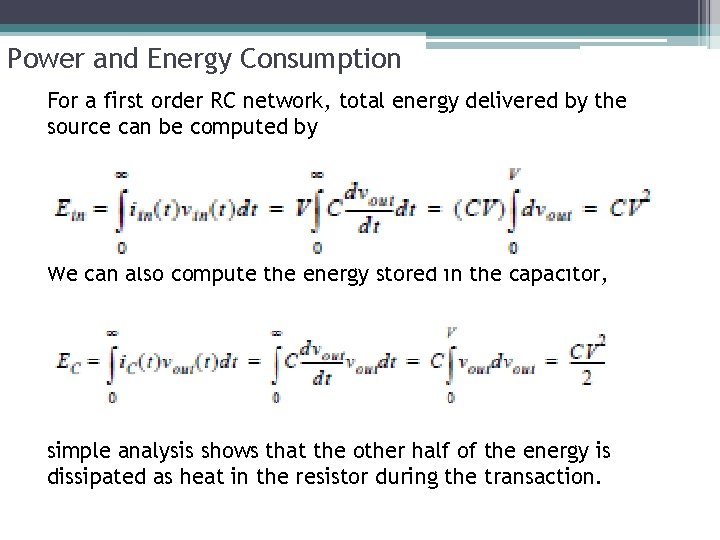
Power and Energy Consumption For a first order RC network, total energy delivered by the source can be computed by We can also compute the energy stored in the capacitor, simple analysis shows that the other half of the energy is dissipated as heat in the resistor during the transaction.