ECE 424 Introduction to VLSI Design Emre Yengel

- Slides: 35

ECE 424 – Introduction to VLSI Design Emre Yengel Department of Electrical and Communication Engineering Fall 2012

Standard Cell Layout Methodology Layout The Design Rules describe: • Minimum width to avoid breaks in a line • Minimum spacing to avoid shorts between lines • Minimum overlap to ensure two layers completely overlap Unit Transistor • Transistor dimensions are specified by their W/L ratio • For 0. 6 μm process, W = 1. 2μm and L = 0. 6μm • Such a minimum width contacted transistor is called UNITTRANSISTOR

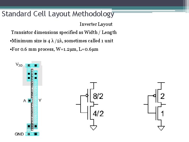
Standard Cell Layout Methodology Inverter Layout Transistor dimensions specified as Width / Length • Minimum size is 4 λ /2λ, sometimes called 1 unit • For 0. 6 mm process, W=1. 2μm, L=0. 6μm

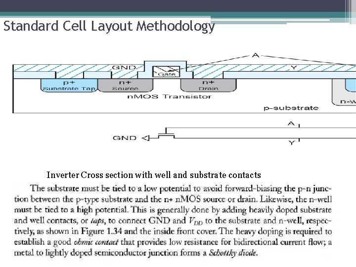
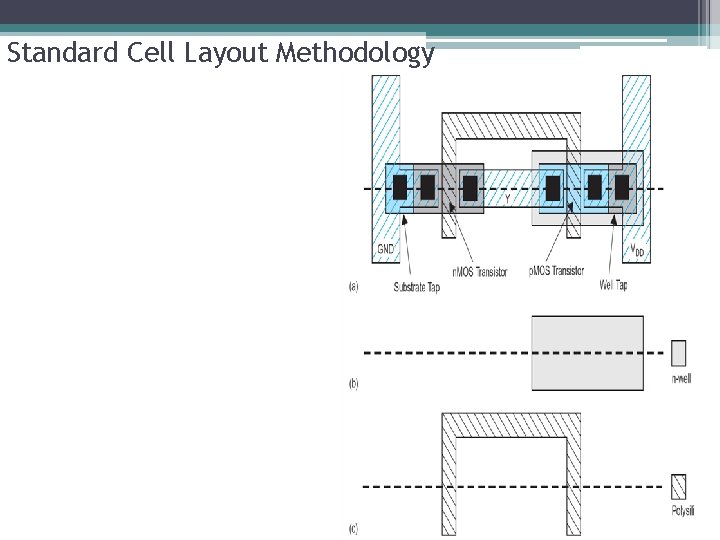
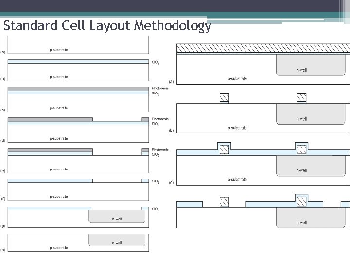
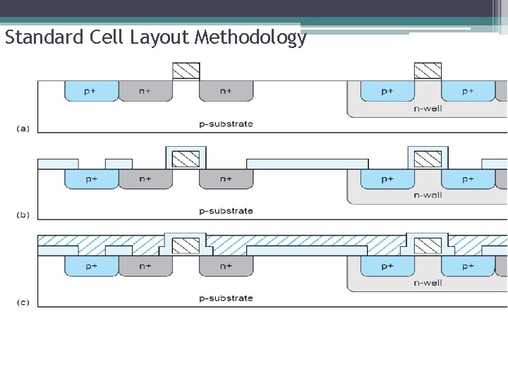
Standard Cell Layout Methodology Inverter Cross section with well and substrate contacts

Standard Cell Layout Methodology

Standard Cell Layout Methodology

Standard Cell Layout Methodology

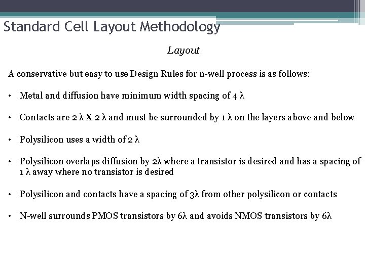
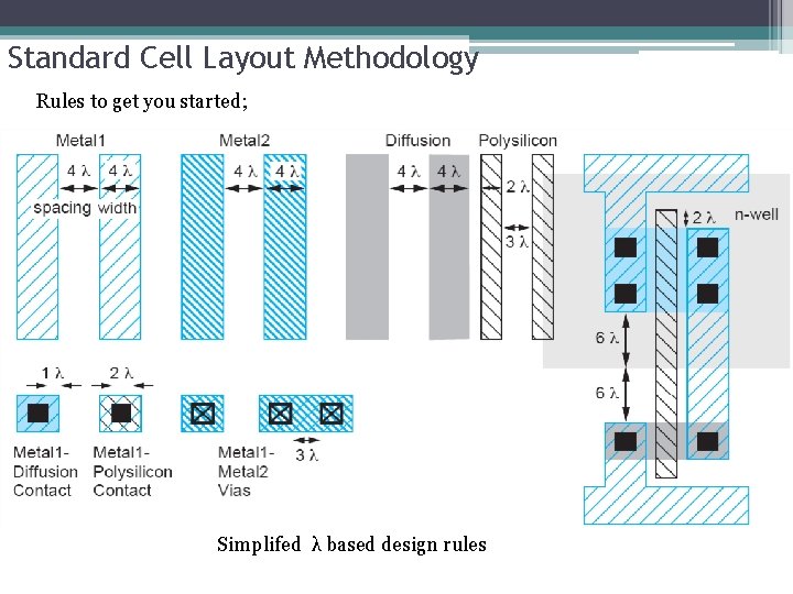
Standard Cell Layout Methodology Layout A conservative but easy to use Design Rules for n-well process is as follows: • Metal and diffusion have minimum width spacing of 4 λ • Contacts are 2 λ X 2 λ and must be surrounded by 1 λ on the layers above and below • Polysilicon uses a width of 2 λ • Polysilicon overlaps diffusion by 2λ where a transistor is desired and has a spacing of 1 λ away where no transistor is desired • Polysilicon and contacts have a spacing of 3λ from other polysilicon or contacts • N-well surrounds PMOS transistors by 6λ and avoids NMOS transistors by 6λ

Standard Cell Layout Methodology Rules to get you started; Simplifed λ based design rules

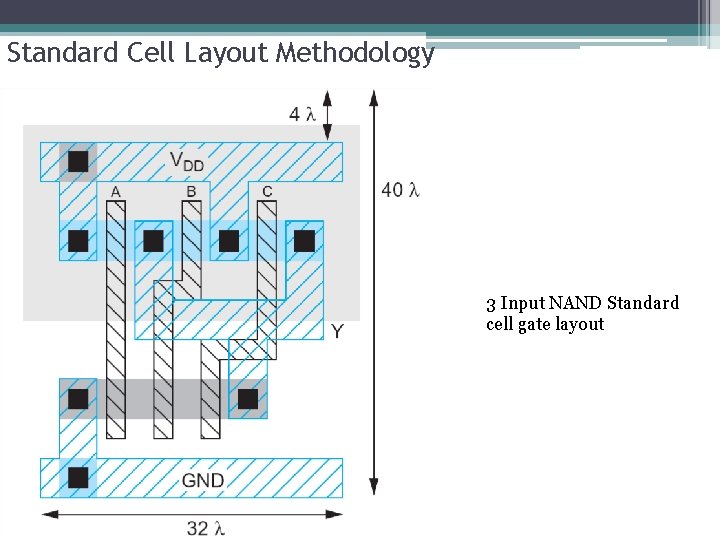
Standard Cell Layout Methodology 3 Input NAND Standard cell gate layout

Standard Cell Layout Methodology Well Spacing: Wells must surround transistors by 6 λ • Implies 12 λ between opposite transistor flavors • Leaves room for one wire track

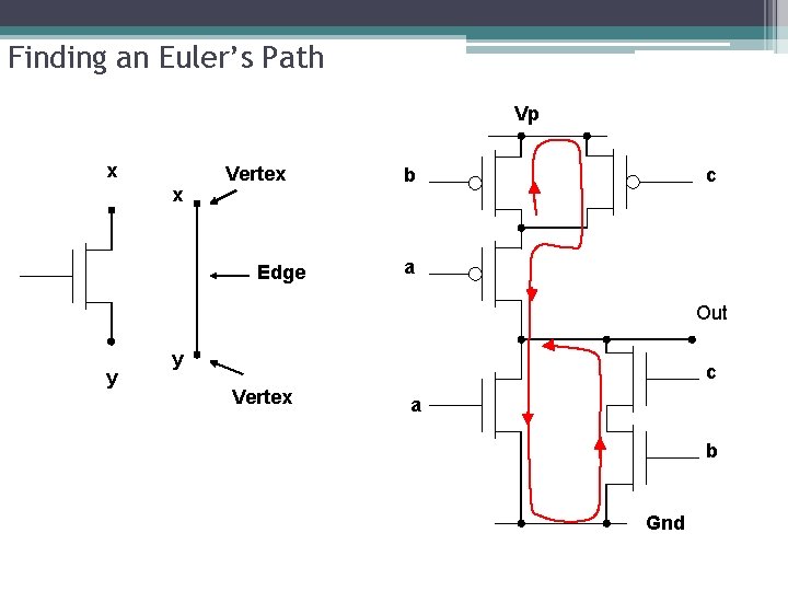
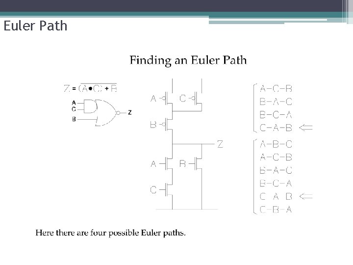
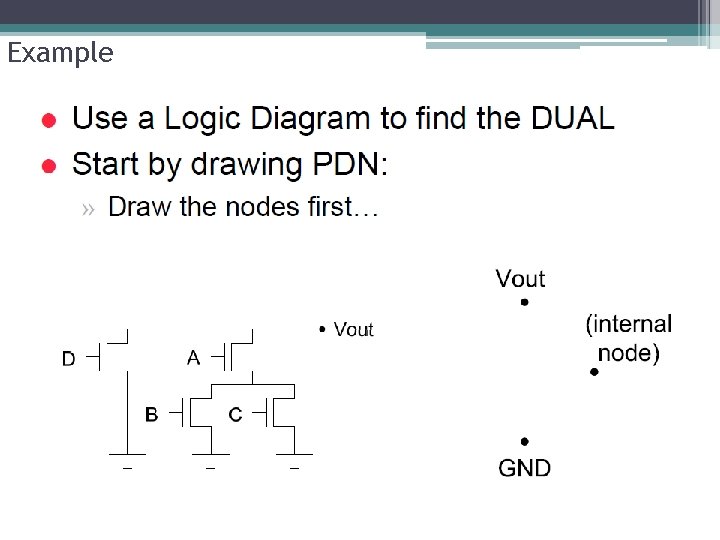
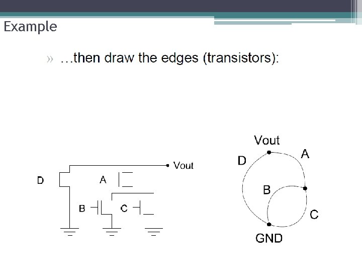
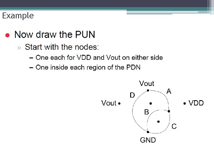
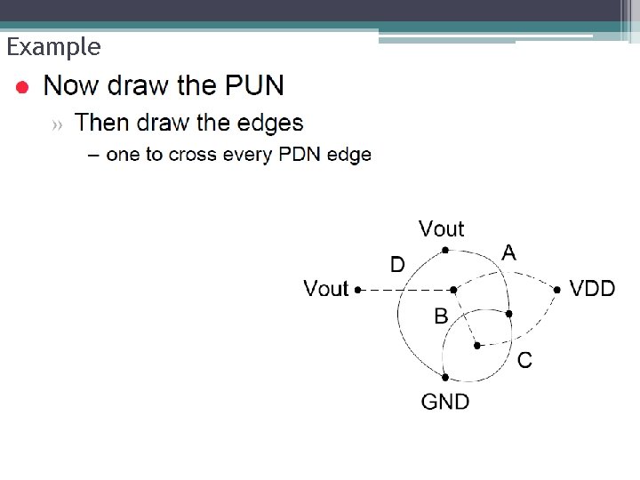
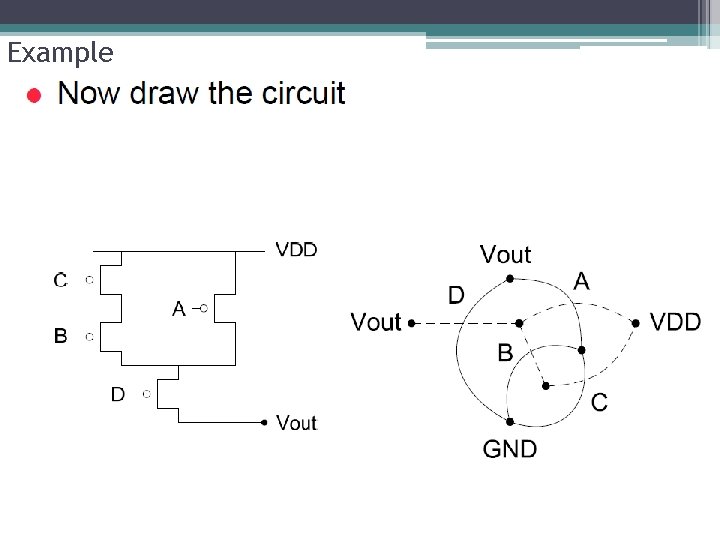
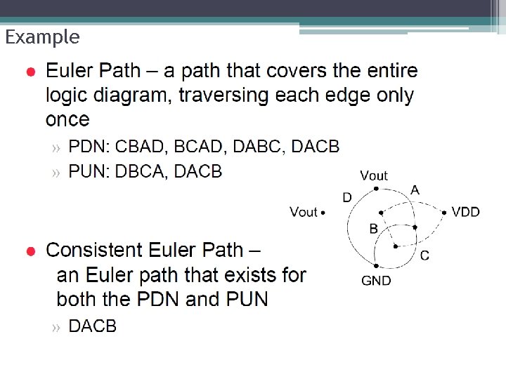
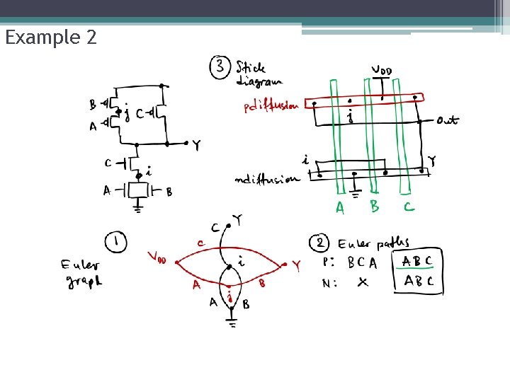
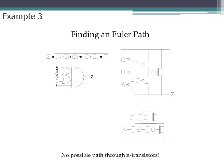
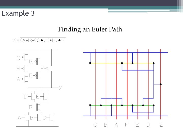
Standard Cell Layout Methodology A simple method for finding the optimum gate ordering is the Euler-path method: Simply find a Euler path in the pull-down network graph and a Euler path in the pull-up network graph with the identical ordering of input labels, i. e. , find a common Euler path for both graphs. The Euler path is defined as an uninterrupted path that traverses each edge (branch) of the graph exactly once.

Finding an Euler’s Path Computer Algorithms: • It is relatively easy for a computer to consider all possible arrangements of transistors in search of a suitable Euler path. This is not so easy for the human designer. One Human Algorithm • Find a path which passes through all n-transistors exactly once. • Express the path in terms of the gate connections. • Is it possible to follow a similarly labelled path through the p-transistors? Ø Yes – you’ve succeeded. Ø No – try again (you may like to try a p path first this time)

Finding an Euler’s Path Vp x x Vertex Edge b c a Out y y c Vertex a b Gnd

Euler Path

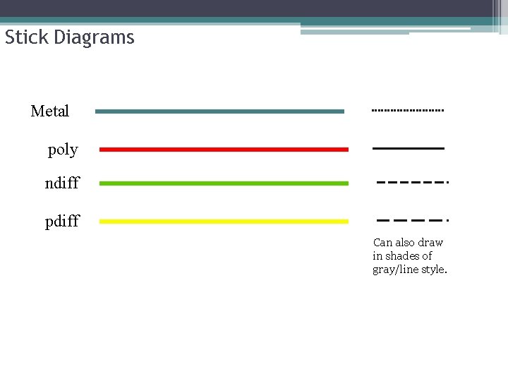
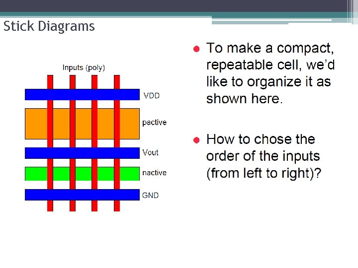
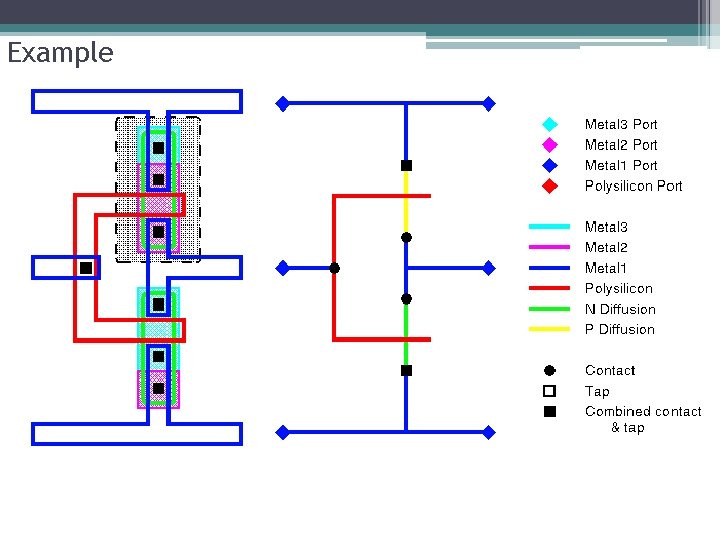
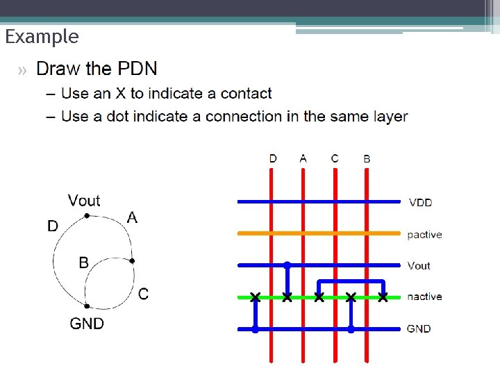
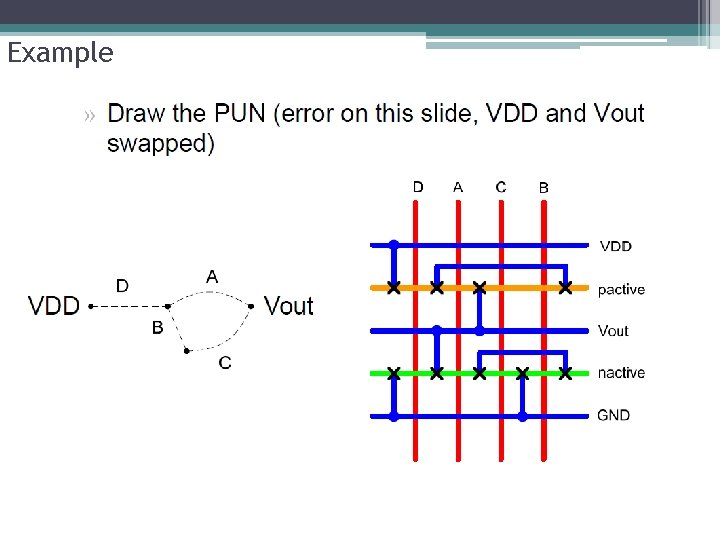
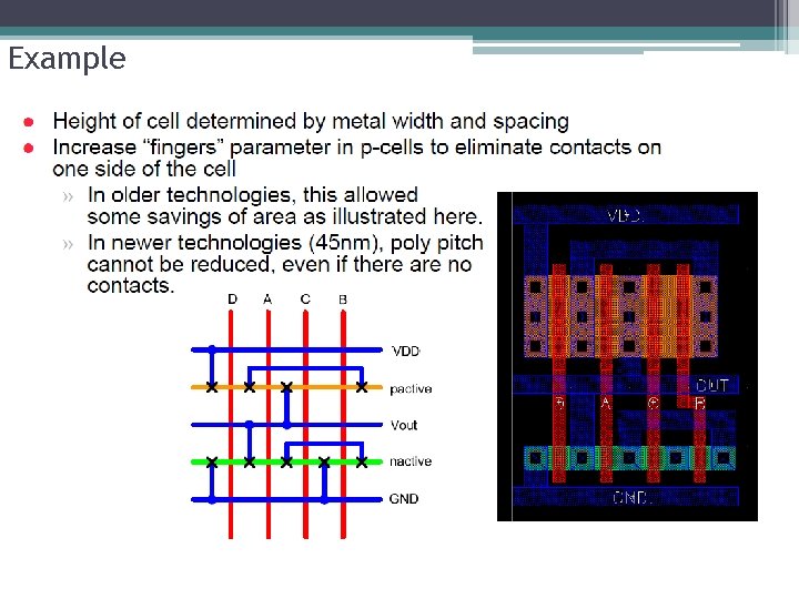
Stick Diagrams (SD) • VLSI design aims to translate circuit concepts onto silicon. • stick diagrams are a means of capturing topography and layer information using simple diagrams. • Stick diagrams convey layer information through colour codes (or monochrome encoding). • Acts as an interface between symbolic circuit and the actual layout.

Stick Diagrams; § Does show all components/vias. § It shows relative placement of components. § Goes one step closer to the layout § Helps plan the layout and routing Stick Diagrams Does not show • Exact placement of components • Transistor sizes • Wire lengths, wire widths, tub boundaries. • Any other low level details such as parasitics.

Stick Diagrams Metal poly ndiff pdiff Can also draw in shades of gray/line style.

Stick Diagrams

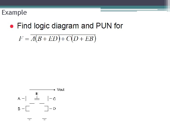
Example

Example

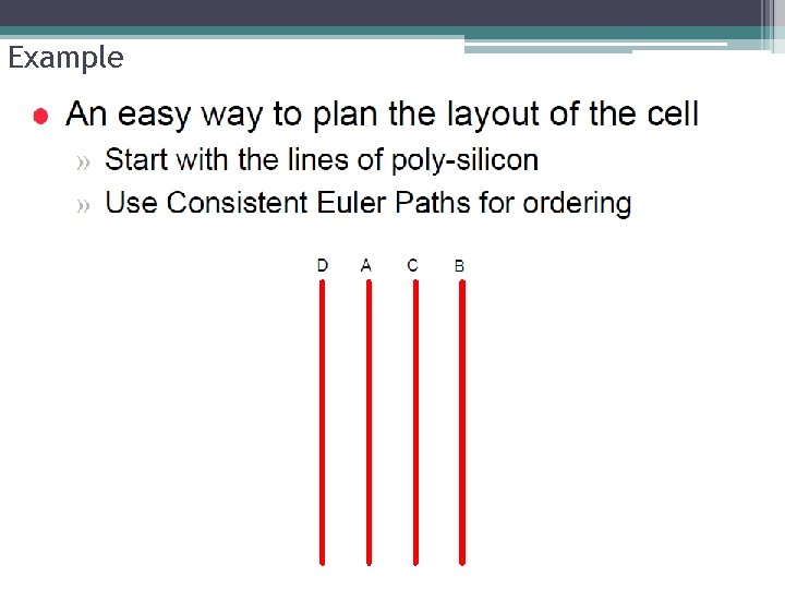
Example

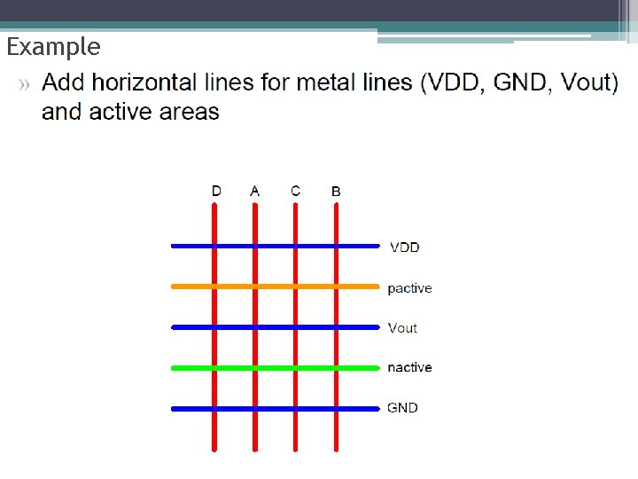
Example

Example

Example

Example

Example

Example

Example

Example

Example

Example

Example 2

Example 3

Example 3