NMOS Inverter EMOSFET Driver and Load Load i
- Slides: 26

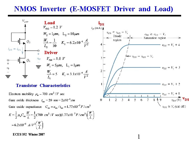
NMOS Inverter (E-MOSFET Driver and Load) Load i. DS Driver Transistor Characteristics v. DS ECES 352 Winter 2007 1

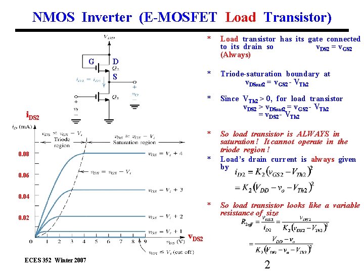
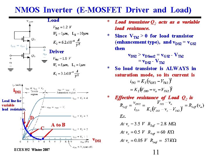
NMOS Inverter (E-MOSFET Load Transistor) G * Load transistor has its gate connected to its drain so v. DS 2 = v. GS 2 (Always) * Triode-saturation boundary at v. DSsat 2 = v. GS 2 - VTh 2 * Since VTh 2 > 0, for load transistor v. DS 2 > v. DSsat 2 = v. GS 2 - VTh 2 = v. DS 2 - VTh 2 * So load transistor is ALWAYS in saturation ! It cannot operate in the triode region ! Load’s drain current is always given by D S i. DS 2 0. 08 * 0. 06 0. 04 * 0. 02 So load transistor looks like a variable resistance of size v. DS 2 ECES 352 Winter 2007 2

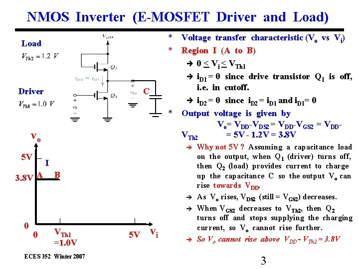
NMOS Inverter (E-MOSFET Driver and Load) * Voltage transfer characteristic (Vo vs Vi) * Region I (A to B) 0 < Vi < VTh 1 i. D 1 = 0 since drive transistor Q 1 is off, i. e. in cutoff. i. D 2 = 0 since i. D 2 = i. D 1 and i. D 1= 0 * Output voltage is given by Vo= VDD-VDS 2 = VDD-VGS 2 = VDDVTh 2 = 5 V - 1. 2 V = 3. 8 V Load Driver C vo 5 V I 3. 8 V A B 0 0 VTh 1 =1. 0 V ECES 352 Winter 2007 5 V vi Why not 5 V ? Assuming a capacitance load on the output, when Q 1 (driver) turns off, then Q 2 (load) provides current to charge up the capacitance C so the output Vo can rise towards VDD. As Vo rises, VDS 2 (still = VGS 2) decreases. When VGS 2 decreases to VTh 2, then Q 2 turns off and stops supplying the charging current, so Vo cannot rise further. So Vo cannot rise above VDD - VTh 2 = 3. 8 V 3

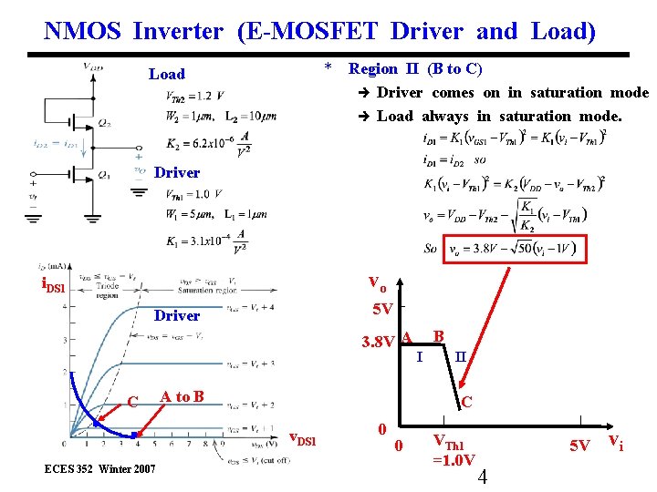
NMOS Inverter (E-MOSFET Driver and Load) * Region II (B to C) Driver comes on in saturation mode Load always in saturation mode. Load Driver vo i. DS 1 5 V Driver 3. 8 V A C A to B I II C v. DS 1 ECES 352 Winter 2007 B 0 0 VTh 1 =1. 0 V 5 V 4 vi

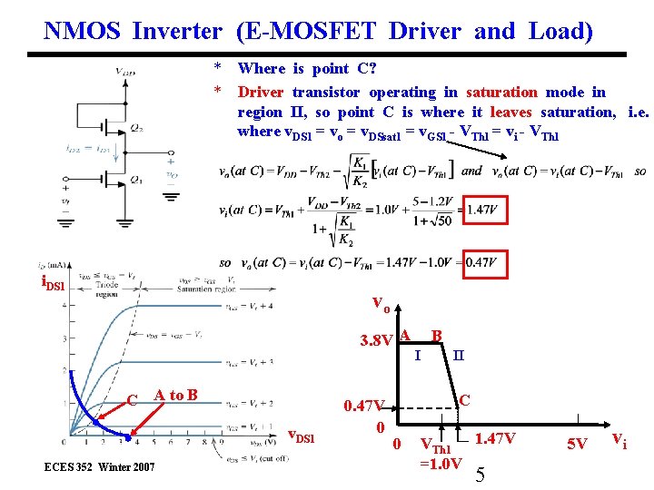
NMOS Inverter (E-MOSFET Driver and Load) * Where is point C? * Driver transistor operating in saturation mode in region II, so point C is where it leaves saturation, i. e. where v. DS 1 = vo = v. DSsat 1 = v. GS 1 - VTh 1 = vi - VTh 1 i. DS 1 vo 3. 8 V A C A to B v. DS 1 ECES 352 Winter 2007 0. 47 V 0 B I II C 0 VTh 1 1. 47 V =1. 0 V 5 5 V vi

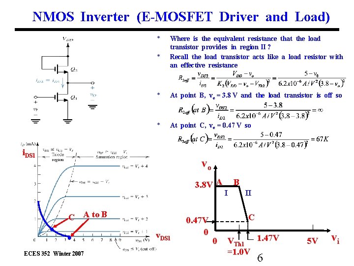
NMOS Inverter (E-MOSFET Driver and Load) * * Where is the equivalent resistance that the load transistor provides in region II ? Recall the load transistor acts like a load resistor with an effective resistance * At point B, vo = 3. 8 V and the load transistor is off so * At point C, vo = 0. 47 V so i. DS 1 vo 3. 8 V A C A to B v. DS 1 ECES 352 Winter 2007 0. 47 V 0 B I II C 0 VTh 1 1. 47 V =1. 0 V 6 5 V vi

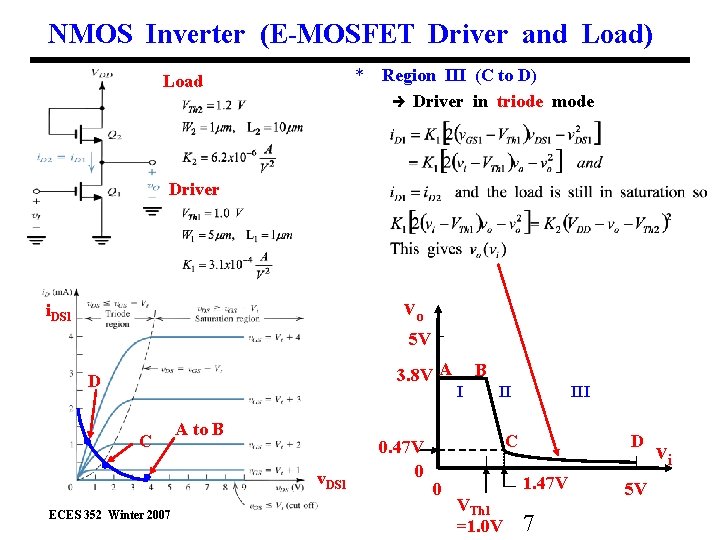
NMOS Inverter (E-MOSFET Driver and Load) * Region III (C to D) Driver in triode mode Load Driver vo i. DS 1 5 V 3. 8 V A D C A to B v. DS 1 ECES 352 Winter 2007 0. 47 V 0 B I II III C 0 D 1. 47 V VTh 1 =1. 0 V 7 5 V vi

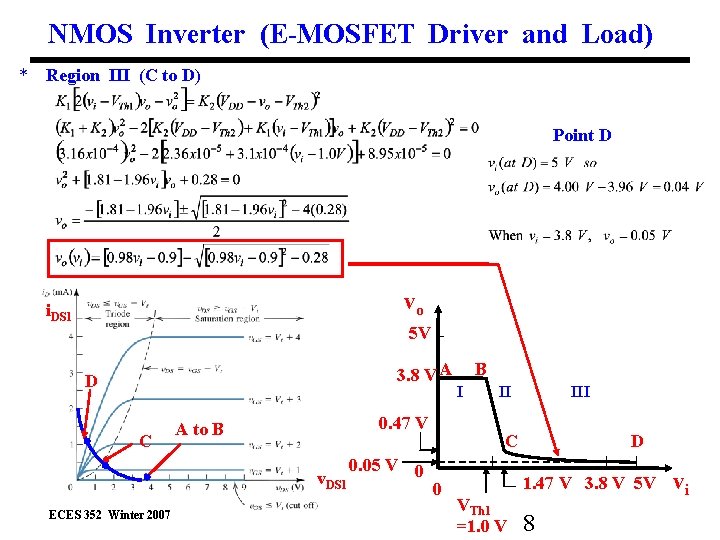
NMOS Inverter (E-MOSFET Driver and Load) * Region III (C to D) Point D vo i. DS 1 5 V 3. 8 V A D C 0. 47 V A to B v. DS 1 ECES 352 Winter 2007 0. 05 V 0 B I II III C 0 D 1. 47 V 3. 8 V 5 V VTh 1 =1. 0 V 8 vi

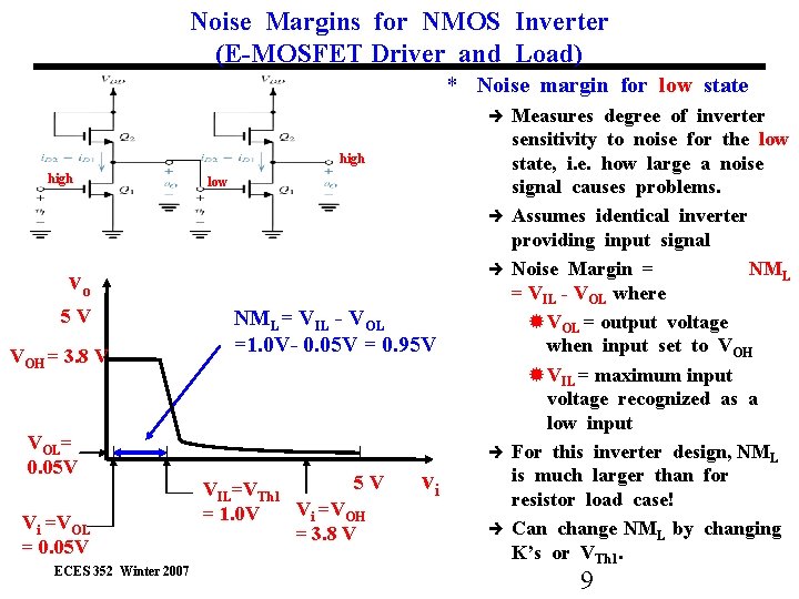
Noise Margins for NMOS Inverter (E-MOSFET Driver and Load) * Noise margin for low state high low vo 5 V VOH = 3. 8 V VOL= 0. 05 V Vi =VOL = 0. 05 V ECES 352 Winter 2007 NML= VIL - VOL =1. 0 V- 0. 05 V = 0. 95 V 5 V VIL=VTh 1 Vi =VOH = 1. 0 V = 3. 8 V vi Measures degree of inverter sensitivity to noise for the low state, i. e. how large a noise signal causes problems. Assumes identical inverter providing input signal Noise Margin = NML = VIL - VOL where VOL = output voltage when input set to VOH VIL = maximum input voltage recognized as a low input For this inverter design, NML is much larger than for resistor load case! Can change NML by changing K’s or VTh 1. 9

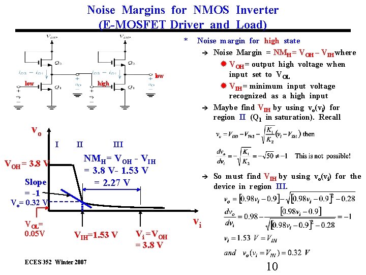
Noise Margins for NMOS Inverter (E-MOSFET Driver and Load) * low high vo I VOH = 3. 8 V Slope = -1 II Noise margin for high state Noise Margin = NMH = VOH – VIH where VOH = output high voltage when input set to VOL VIH = minimum input voltage recognized as a high input Maybe find VIH by using vo(vi) for region II (Q 1 in saturation). Recall III NMH= VOH - VIH = 3. 8 V- 1. 53 V = 2. 27 V So must find VIH by using vo(vi) for the device in region III. Vo= 0. 32 V VOL= 0. 05 V VIH=1. 53 V ECES 352 Winter 2007 Vi =VOH = 3. 8 V vi 10

NMOS Inverter (E-MOSFET Driver and Load) Load * Load transistor Q 2 acts as a variable load resistance. * Since VTh 2 > 0 for load transistor (enhancement type), and v. DS 2 = v. GS 2 then v. DS 2 > v. DSsat 2 = v. GS 2 - VTh 2 = v. DS 2 - VTh 2 * So load transistor is ALWAYS in saturation mode, so its current is Driver i. DS 1 * Effective resistance of Load Q 2 is Load line for variable load resistance. D C A to B v. DS 1 ECES 352 Winter 2007 11

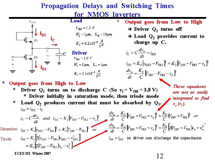
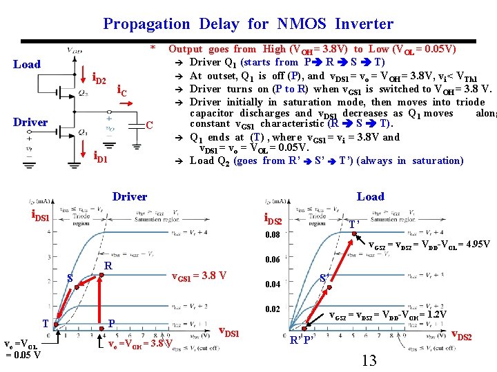
Propagation Delays and Switching Times for NMOS Inverters Load i. D 2 i. C C * Output goes from Low to High Driver Q 1 turns off Load Q 2 provides current to charge up C. Driver i. D 1 * Output goes from High to Low * Driver Q 1 turns on to discharge C (So vi = VOH = 3. 8 V) * Driver initially in saturation mode, then triode mode * Load Q 2 produces current that must be absorbed by Q 1. Saturation Triode ECES 352 Winter 2007 12 These equations are not as easily integrated to find vo (vi ).

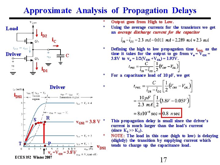
Propagation Delay for NMOS Inverter * Load i. D 2 i. C Driver C i. D 1 Output goes from High (VOH = 3. 8 V) to Low (VOL = 0. 05 V) Driver Q 1 (starts from P R S T) At outset, Q 1 is off (P), and v. DS 1 = vo = VOH = 3. 8 V, vi < VTh 1 Driver turns on (P to R) when v. GS 1 is switched to VOH = 3. 8 V. Driver initially in saturation mode, then moves into triode capacitor discharges and v. DS 1 decreases as Q 1 moves along constant v. GS 1 characteristic (R S T). Q 1 ends at (T) , where v. GS 1 = vi = 3. 8 V and v. DS 1 = vo = VOL = 0. 05 V. Load Q 2 (goes from R’ S’ T’) (always in saturation) Driver Load i. DS 1 i. DS 2 T’ 0. 08 R S v. GS 2 = v. DS 2 = VDD-VOL = 4. 95 V 0. 06 v. GS 1 = 3. 8 V S’ 0. 04 0. 02 T P vo =VOL vo =VOH = 3. 8 V ECES 352 Winter 2007 = 0. 05 V v. DS 1 v. GS 2 = v. DS 2 = VDD-VOH = 1. 2 V v. DS 2 R’ P’ 13

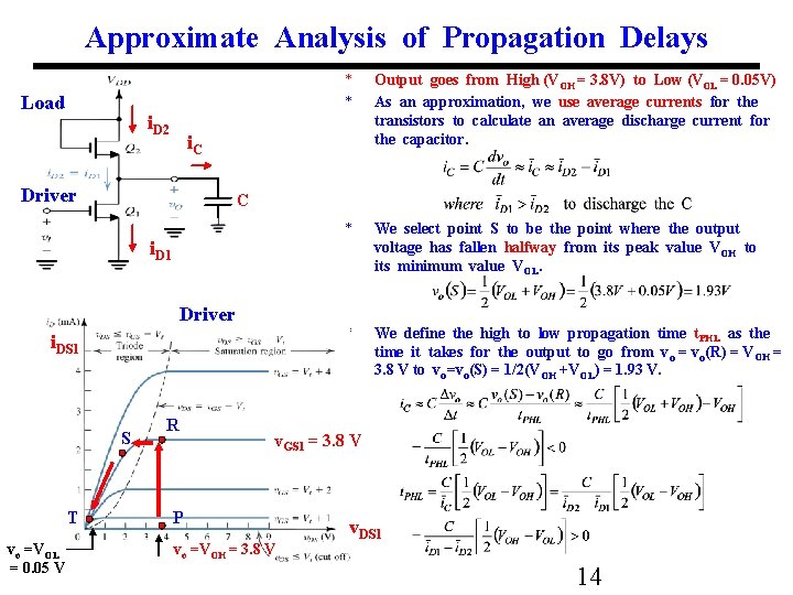
Approximate Analysis of Propagation Delays Load i. D 2 Output goes from High (VOH = 3. 8 V) to Low (VOL = 0. 05 V) As an approximation, we use average currents for the transistors to calculate an average discharge current for the capacitor. * We select point S to be the point where the output voltage has fallen halfway from its peak value VOH to its minimum value VOL. * We define the high to low propagation time t. PHL as the time it takes for the output to go from vo = vo(R) = VOH = 3. 8 V to vo=vo(S) = 1/2(VOH +VOL) = 1. 93 V. i. C Driver C i. D 1 Driver i. DS 1 S T * * R v. GS 1 = 3. 8 V P vo =VOL vo =VOH = 3. 8 V ECES 352 Winter 2007 = 0. 05 V v. DS 1 14

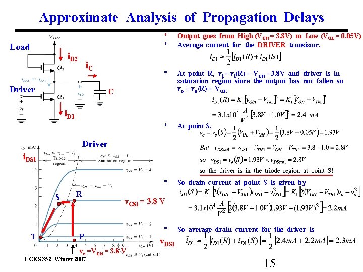
Approximate Analysis of Propagation Delays Load i. D 2 i. C Driver * * Output goes from High (VOH = 3. 8 V) to Low (VOL = 0. 05 V) Average current for the DRIVER transistor. * At point R, vi = vi(R) = VOH =3. 8 V and driver is in saturation region since the output has not fallen so vo = vo(R) = VOH * At point S, * So drain current at point S is given by C i. D 1 Driver i. DS 1 S T R v. GS 1 = 3. 8 V P vo =VOH = 3. 8 V ECES 352 Winter 2007 * So average drain current for the driver is v. DS 1 15

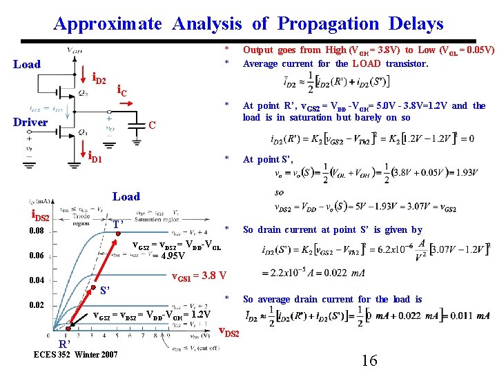
Approximate Analysis of Propagation Delays Load i. D 2 * * Output goes from High (VOH = 3. 8 V) to Low (VOL = 0. 05 V) Average current for the LOAD transistor. * At point R’, v. GS 2 = VDD -VOH= 5. 0 V - 3. 8 V=1. 2 V and the load is in saturation but barely on so * At point S’, * So drain current at point S’ is given by i. C Driver C i. D 1 Load i. DS 2 T’ 0. 08 v. GS 2 = v. DS 2 = VDD-VOL = 4. 95 V 0. 06 v. GS 1 = 3. 8 V 0. 04 S’ 0. 02 * So average drain current for the load is v. GS 2 = v. DS 2 = VDD-VOH = 1. 2 V R’ ECES 352 Winter 2007 v. DS 2 16

Approximate Analysis of Propagation Delays Load i. D 2 * * Output goes from High to Low. Using the average currents for the transistors we get an average discharge current for the capacitor * Defining the high to low propagation time t. PHL as the time it takes for the output to go from vo = VOH = 3. 8 V to vo = 1/2(VOH +VOL) = 1. 93 V. * For a capacitance load of 10 p. F, we get i. C Driver C i. D 1 Driver * i. DS 1 S R v. GS 1 = 3. 8 V * * T P vo =VOH = 3. 8 V ECES 352 Winter 2007 v. DS 1 This propagation delay is small since the driver’s current is much larger than the load’s current (since K 1 >> K 2). NOTE: The load in this case (high to low) is delaying (slightly) the transition by supplying current which tends to charge up the capacitance load. 17

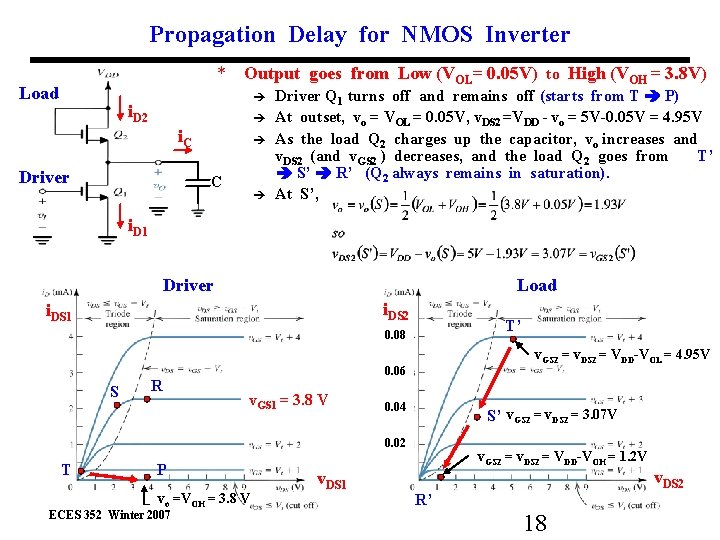
Propagation Delay for NMOS Inverter * Output goes from Low (VOL= 0. 05 V) to High (VOH = 3. 8 V) Load i. D 2 i. C Driver Q 1 turns off and remains off (starts from T P) At outset, vo = VOL = 0. 05 V, v. DS 2 =VDD - vo = 5 V-0. 05 V = 4. 95 V As the load Q 2 charges up the capacitor, vo increases and v. DS 2 (and v. GS 2 ) decreases, and the load Q 2 goes from T’ S’ R’ (Q 2 always remains in saturation). At S’, i. D 1 Driver Load i. DS 2 i. DS 1 T’ 0. 08 S R v. GS 2 = v. DS 2 = VDD-VOL = 4. 95 V 0. 06 v. GS 1 = 3. 8 V 0. 04 S’ v. GS 2 = v. DS 2 = 3. 07 V 0. 02 T P vo =VOH = 3. 8 V ECES 352 Winter 2007 v. DS 1 v. GS 2 = v. DS 2 = VDD-VOH = 1. 2 V v. DS 2 R’ 18

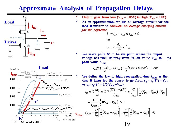
Approximate Analysis of Propagation Delays Load i. D 2 * * Output goes from Low (VOL = 0. 05 V) to High (VOH = 3. 8 V). As an approximation, we use an average current for the load transistor to calculate an average charging current for the capacitor. * We select point S’ to be the point where the output voltage has risen halfway from its low value VOL to peak value VOH. i. C Driver C i. D 1 its Load i. DS 2 * T’ 0. 08 v. GS 2 = v. DS 2 = VDD-VOL = 4. 95 V 0. 06 We define the low to high propagation time t. PLH as the time it takes for the output to go from vo = vo(T’) = VOL to vo=vo(S’) = 1/2(VOH +VOL). 0. 04 S’ 0. 02 v. GS 2 = v. DS 2 = VDD-VOH = 1. 2 V R’ ECES 352 Winter 2007 v. DS 2 19

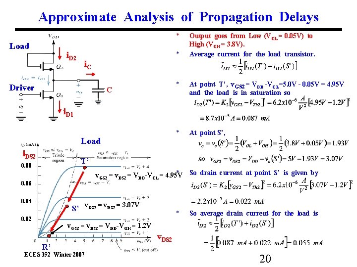
Approximate Analysis of Propagation Delays * Load i. D 2 * Output goes from Low (VOL = 0. 05 V) to High (VOH = 3. 8 V). Average current for the load transistor. i. C Driver C * At point T’, v. GS 2 = VDD -VOL=5. 0 V - 0. 05 V = 4. 95 V and the load is in saturation so * At point S’, i. D 1 Load i. DS 2 T’ 0. 08 * So drain current at point S’ is given by v. GS 2 = v. DS 2 = VDD-VOL = 4. 95 V 0. 06 0. 04 S’ v. GS 2 = v. DS 2 = 3. 07 V 0. 02 * So average drain current for the load is v. GS 2 = v. DS 2 = VDD-VOH = 1. 2 V R’ ECES 352 Winter 2007 v. DS 2 20

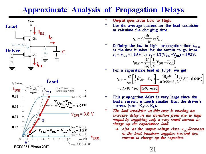
Approximate Analysis of Propagation Delays Load i. D 2 * * Output goes from Low to High. Use the average current for the load transistor to calculate the charging time. * Defining the low to high propagation time t. PLH as the time it takes for the output to go from vo = VOL = 0. 05 V to vo = 1/2(VOH +VOL) = 1. 93 V. * For a capacitance load of 10 p. F, we get * This propagation delay is very large since the load’s current is much smaller than the driver’s current (since K 2 << K 1). The load transistor in this case is causing an excessive delay in the transition from low to high output by supplying only a very small current to charge up the capacitance load. Also, as the output voltage rises, vgs 2 decreases so the load transistor supplies less and less current to charge up the capacitor. i. C Driver C i. D 1 Load i. DS 2 T’ 0. 08 v. GS 2 = v. DS 2 = VDD-VOL = 4. 95 V 0. 06 v. GS 1 = 3. 8 V 0. 04 S’ 0. 02 v. GS 2 = v. DS 2 = VDD-VOH = 1. 2 V R’ ECES 352 Winter 2007 v. DS 2 * 21

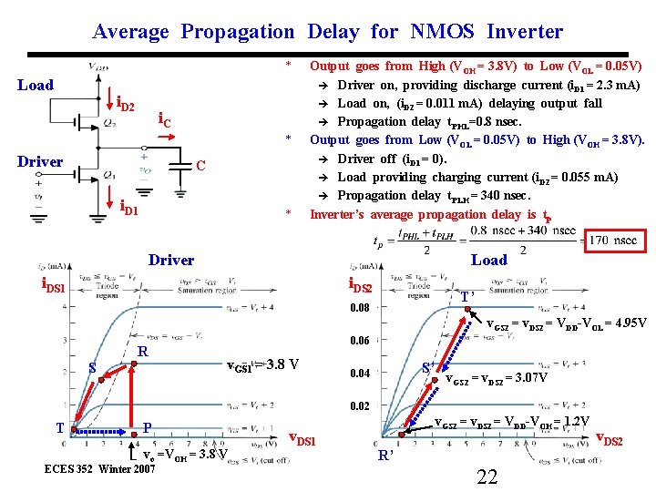
Average Propagation Delay for NMOS Inverter * Load i. D 2 i. C * Driver C i. D 1 * Output goes from High (VOH = 3. 8 V) to Low (VOL = 0. 05 V) Driver on, providing discharge current (i. D 1 = 2. 3 m. A) Load on, (i. D 2 = 0. 011 m. A) delaying output fall Propagation delay t. PHL=0. 8 nsec. Output goes from Low (VOL = 0. 05 V) to High (VOH = 3. 8 V). Driver off (i. D 1 = 0). Load providing charging current (i. D 2 = 0. 055 m. A) Propagation delay t. PLH = 340 nsec. Inverter’s average propagation delay is tp Driver Load i. DS 1 i. DS 2 T’ 0. 08 v. GS 2 = v. DS 2 = VDD-VOL = 4. 95 V R S 0. 06 v. GS 1 = 3. 8 V S’ 0. 04 v. GS 2 = v. DS 2 = 3. 07 V 0. 02 T P vo =VOH = 3. 8 V ECES 352 Winter 2007 v. DS 1 v. GS 2 = v. DS 2 = VDD-VOH = 1. 2 V R’ 22 v. DS 2

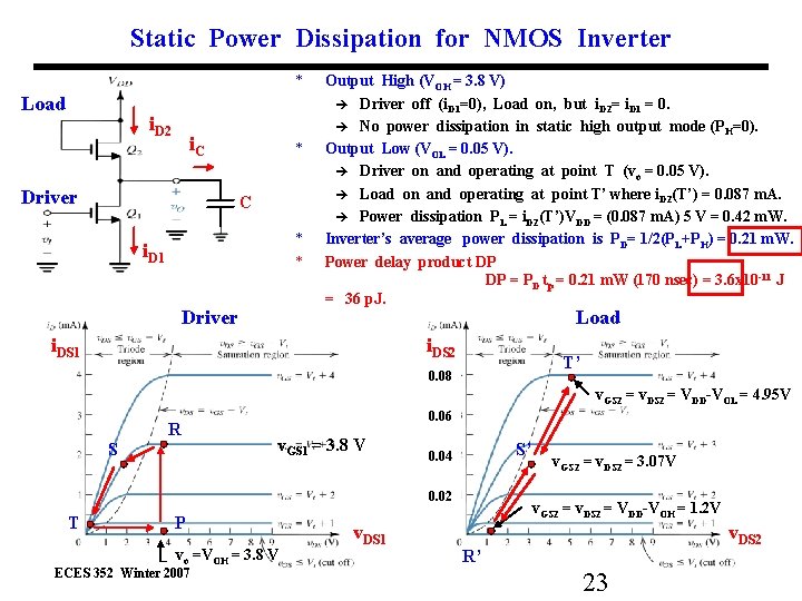
Static Power Dissipation for NMOS Inverter * Load i. D 2 i. C Driver * C * * i. D 1 Driver Output High (VOH = 3. 8 V) Driver off (i. D 1=0), Load on, but i. D 2= i. D 1 = 0. No power dissipation in static high output mode (PH=0). Output Low (VOL = 0. 05 V). Driver on and operating at point T (vo = 0. 05 V). Load on and operating at point T’ where i. D 2(T’) = 0. 087 m. A. Power dissipation PL = i. D 2(T’)VDD = (0. 087 m. A) 5 V = 0. 42 m. W. Inverter’s average power dissipation is PD= 1/2(PL+PH) = 0. 21 m. W. Power delay product DP DP = PD tp = 0. 21 m. W (170 nsec) = 3. 6 x 10 -11 J = 36 p. J. Load i. DS 1 i. DS 2 T’ 0. 08 v. GS 2 = v. DS 2 = VDD-VOL = 4. 95 V R S 0. 06 v. GS 1 = 3. 8 V S’ 0. 04 0. 02 T P vo =VOH = 3. 8 V ECES 352 Winter 2007 v. DS 1 v. GS 2 = v. DS 2 = 3. 07 V v. GS 2 = v. DS 2 = VDD-VOH = 1. 2 V v. DS 2 R’ 23

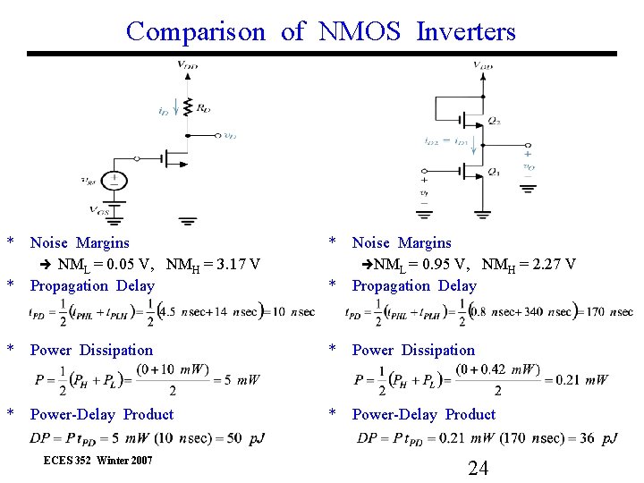
Comparison of NMOS Inverters * Noise Margins NML = 0. 05 V, NMH = 3. 17 V * Propagation Delay * Noise Margins NML = 0. 95 V, NMH = 2. 27 V * Propagation Delay * Power Dissipation * Power-Delay Product ECES 352 Winter 2007 24

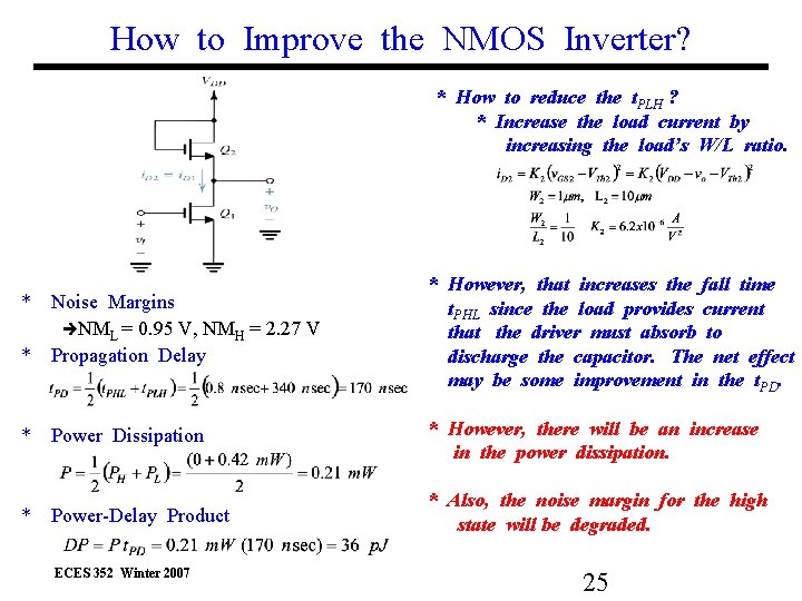
How to Improve the NMOS Inverter? * How to reduce the t. PLH ? * Increase the load current by increasing the load’s W/L ratio. * Noise Margins NML = 0. 95 V, NMH = 2. 27 V * Propagation Delay * However, that increases the fall time t. PHL since the load provides current that the driver must absorb to discharge the capacitor. The net effect may be some improvement in the t. PD. * Power Dissipation * However, there will be an increase in the power dissipation. * Power-Delay Product * Also, the noise margin for the high state will be degraded. ECES 352 Winter 2007 25

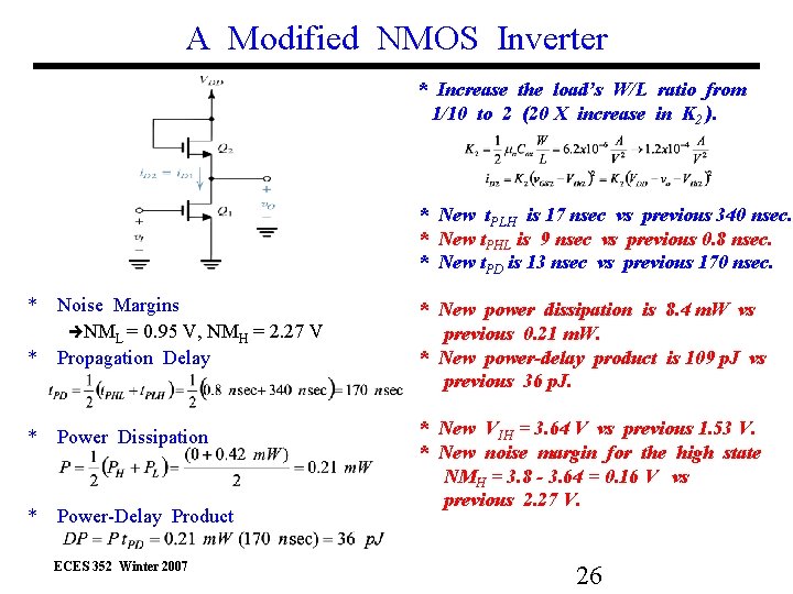
A Modified NMOS Inverter * Increase the load’s W/L ratio from 1/10 to 2 (20 X increase in K 2 ). * New t. PLH is 17 nsec vs previous 340 nsec. * New t. PHL is 9 nsec vs previous 0. 8 nsec. * New t. PD is 13 nsec vs previous 170 nsec. * Noise Margins NML = 0. 95 V, NMH = 2. 27 V * Propagation Delay * New power dissipation is 8. 4 m. W vs previous 0. 21 m. W. * New power-delay product is 109 p. J vs previous 36 p. J. * Power Dissipation * New VIH = 3. 64 V vs previous 1. 53 V. * New noise margin for the high state NMH = 3. 8 - 3. 64 = 0. 16 V vs previous 2. 27 V. * Power-Delay Product ECES 352 Winter 2007 26