Digital Design Chapter 9 Hardware Description Languages Slides
- Slides: 53

Digital Design Chapter 9: Hardware Description Languages Slides to accompany the textbook Digital Design, First Edition, by Frank Vahid, John Wiley and Sons Publishers, 2007. http: //www. ddvahid. com Copyright © 2007 Frank Vahid Instructors of courses requiring Vahid's Digital Design textbook (published by John Wiley and Sons) have permission to modify and use these slides for customary course-related activities, subject to keeping this copyright notice in place and unmodified. These slides may be posted as unanimated pdf versions on publicly-accessible course websites. . Power. Point source (or pdf Digital Design with animations) may not be posted to publicly-accessible websites, but may be posted for students on internal protected sites or distributed directly to students by other electronic means. Copyright © 2006 1 Instructors may make printouts of the slides available to students for a reasonable photocopying charge, without incurring royalties. Any other use requires explicit permission. Instructors Franksource Vahid may obtain Power. Point or obtain special use permissions from Wiley – see http: //www. ddvahid. com for information.

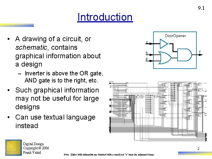
9. 1 Introduction Door. Opener • A drawing of a circuit, or schematic, contains graphical information about a design c – Inverter is above the OR gate, AND gate is to the right, etc. • Such graphical information may not be useful for large designs • Can use textual language instead Digital Design Copyright © 2006 Frank Vahid f h p si a tap a rtn o co t g 2 Note: Slides with animation are denoted with a small red "a" near the animated items

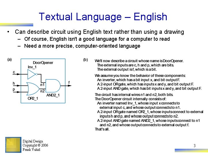
Textual Language – English • Can describe circuit using English text rather than using a drawing – Of course, English isn't a good language for a computer to read – Need a more precise, computer-oriented language Digital Design Copyright © 2006 Frank Vahid 3

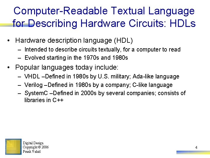
Computer-Readable Textual Language for Describing Hardware Circuits: HDLs • Hardware description language (HDL) – Intended to describe circuits textually, for a computer to read – Evolved starting in the 1970 s and 1980 s • Popular languages today include: – VHDL –Defined in 1980 s by U. S. military; Ada-like language – Verilog –Defined in 1980 s by a company; C-like language – System. C –Defined in 2000 s by several companies; consists of libraries in C++ Digital Design Copyright © 2006 Frank Vahid 4

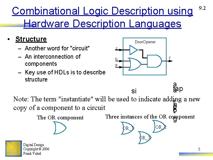
Combinational Logic Description using Hardware Description Languages • Structure 9. 2 Door. Opener – Another word for "circuit" – An interconnection of components – Key use of HDLs is to describe structure c f h p a tap a si Note: The term "instantiate" will be used to indicate adding rtn a new o co copy of a component to a circuit t The OR component Three instances of the OR component g OR_2 OR_1 OR_3 Digital Design Copyright © 2006 Frank Vahid 5

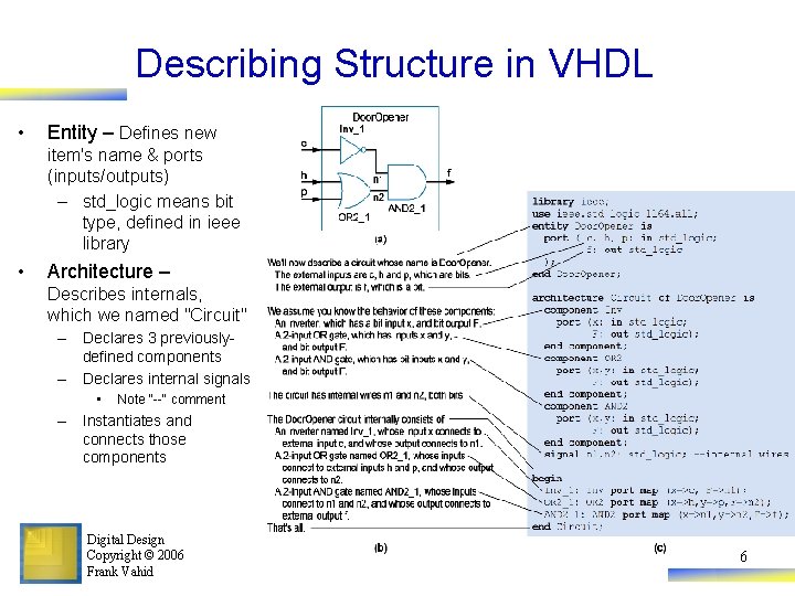
Describing Structure in VHDL • Entity – Defines new item's name & ports (inputs/outputs) – std_logic means bit type, defined in ieee library • Architecture – Describes internals, which we named "Circuit" – Declares 3 previouslydefined components – Declares internal signals • Note "--" comment – Instantiates and connects those components Digital Design Copyright © 2006 Frank Vahid 6

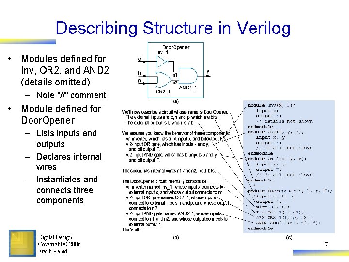
Describing Structure in Verilog • Modules defined for Inv, OR 2, and AND 2 (details omitted) – Note "//" comment • Module defined for Door. Opener – Lists inputs and outputs – Declares internal wires – Instantiates and connects three components Digital Design Copyright © 2006 Frank Vahid 7

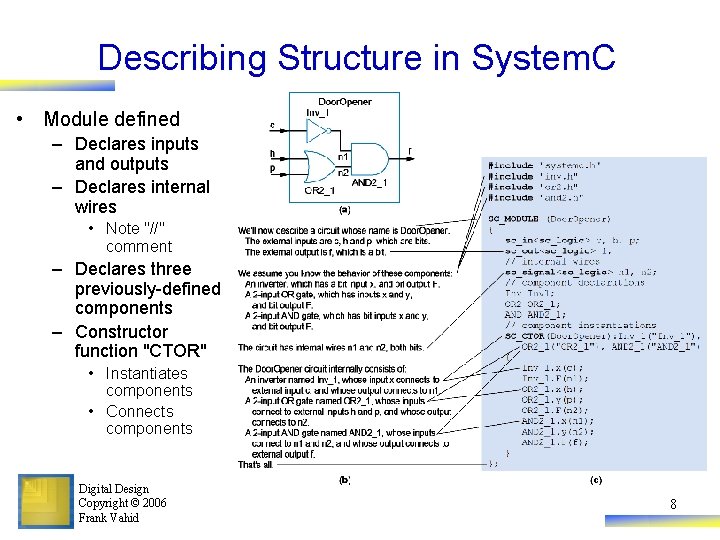
Describing Structure in System. C • Module defined – Declares inputs and outputs – Declares internal wires • Note "//" comment – Declares three previously-defined components – Constructor function "CTOR" • Instantiates components • Connects components Digital Design Copyright © 2006 Frank Vahid 8

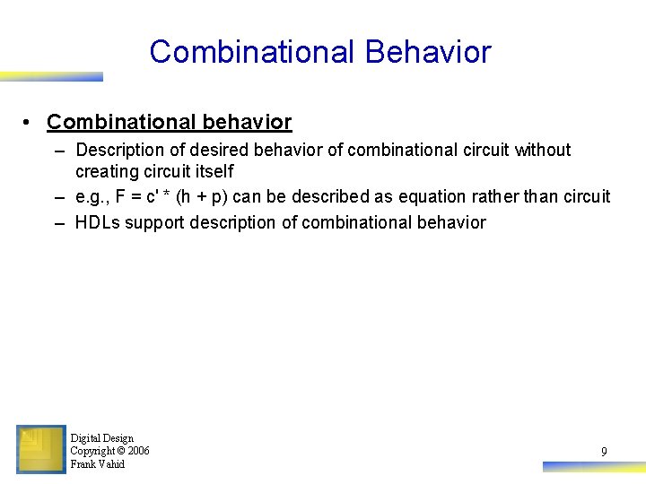
Combinational Behavior • Combinational behavior – Description of desired behavior of combinational circuit without creating circuit itself – e. g. , F = c' * (h + p) can be described as equation rather than circuit – HDLs support description of combinational behavior Digital Design Copyright © 2006 Frank Vahid 9

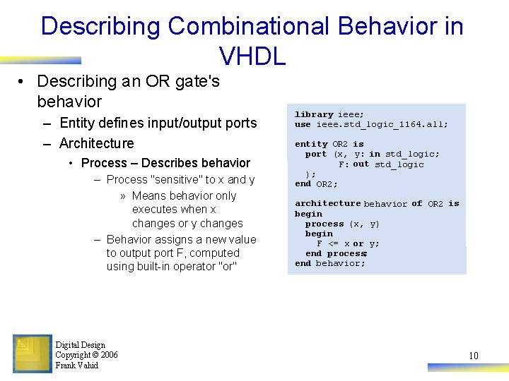
Describing Combinational Behavior in VHDL • Describing an OR gate's behavior – Entity defines input/output ports – Architecture • Process – Describes behavior – Process "sensitive" to x and y » Means behavior only executes when x changes or y changes – Behavior assigns a new value to output port F, computed using built-in operator "or" Digital Design Copyright © 2006 Frank Vahid library ieee; use ieee. std_logic_1164. all; entity OR 2 is port (x, y: in std_logic; F: out std_logic ); end OR 2; architecture behavior of OR 2 is begin process (x, y) begin F <= x or y; end process; end behavior; 10

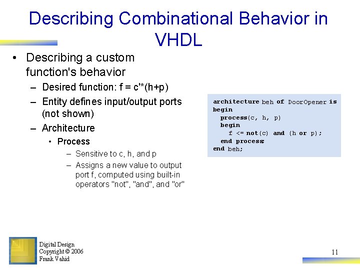
Describing Combinational Behavior in VHDL • Describing a custom function's behavior – Desired function: f = c'*(h+p) – Entity defines input/output ports (not shown) – Architecture • Process – Sensitive to c, h, and p – Assigns a new value to output port f, computed using built-in operators "not", "and", and "or" Digital Design Copyright © 2006 Frank Vahid architecture beh of Door. Opener is begin process(c, h, p) begin f <= not(c) and (h or p); end process; end beh; 11

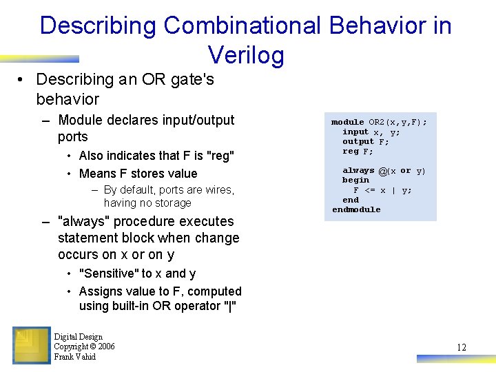
Describing Combinational Behavior in Verilog • Describing an OR gate's behavior – Module declares input/output ports • Also indicates that F is "reg" • Means F stores value – By default, ports are wires, having no storage – "always" procedure executes statement block when change occurs on x or on y module OR 2(x, y, F); input x, y; output F; reg F; always @(x or y) begin F <= x | y; endmodule • "Sensitive" to x and y • Assigns value to F, computed using built-in OR operator "|" Digital Design Copyright © 2006 Frank Vahid 12

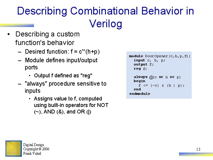
Describing Combinational Behavior in Verilog • Describing a custom function's behavior – Desired function: f = c'*(h+p) – Module defines input/output ports • Output f defined as "reg" – "always" procedure sensitive to inputs • Assigns value to f, computed using built-in operators for NOT (~), AND (&), and OR (|) Digital Design Copyright © 2006 Frank Vahid module Door. Opener(c, h, p, f); input c, h, p; output f; reg f; always @(c or h or p) begin f <= (~c) & (h | p); endmodule 13

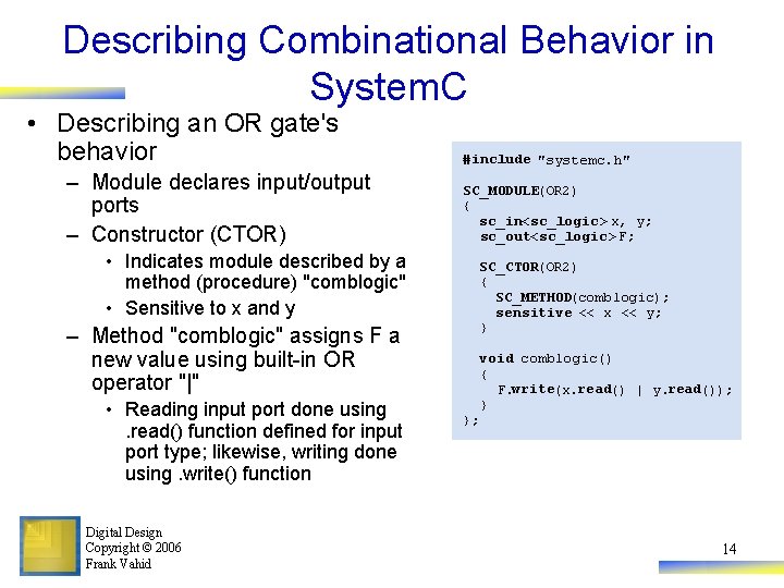
Describing Combinational Behavior in System. C • Describing an OR gate's behavior – Module declares input/output ports – Constructor (CTOR) • Indicates module described by a method (procedure) "comblogic" • Sensitive to x and y – Method "comblogic" assigns F a new value using built-in OR operator "|" • Reading input port done using. read() function defined for input port type; likewise, writing done using. write() function Digital Design Copyright © 2006 Frank Vahid #include "systemc. h" SC_MODULE(OR 2) { sc_in<sc_logic> x, y; sc_out<sc_logic> F; SC_CTOR(OR 2) { SC_METHOD(comblogic); sensitive << x << y; } void comblogic() { F. write(x. read() | y. read()); } }; 14

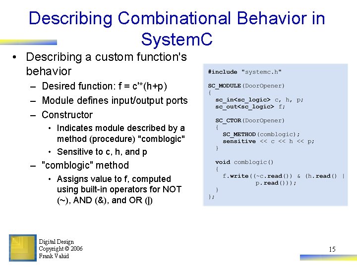
Describing Combinational Behavior in System. C • Describing a custom function's behavior – Desired function: f = c'*(h+p) – Module defines input/output ports – Constructor • Indicates module described by a method (procedure) "comblogic" • Sensitive to c, h, and p – "comblogic" method • Assigns value to f, computed using built-in operators for NOT (~), AND (&), and OR (|) Digital Design Copyright © 2006 Frank Vahid 15

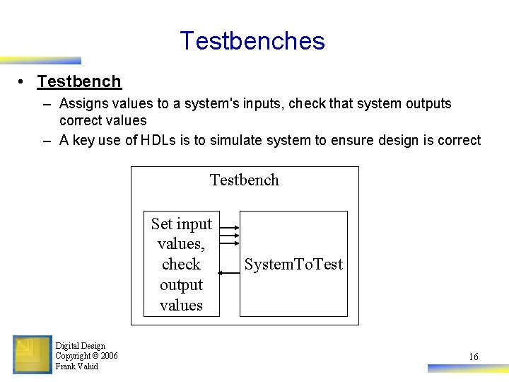
Testbenches • Testbench – Assigns values to a system's inputs, check that system outputs correct values – A key use of HDLs is to simulate system to ensure design is correct Testbench Set input values, check output values Digital Design Copyright © 2006 Frank Vahid System. To. Test 16

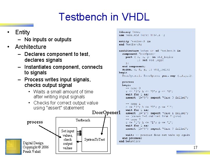
Testbench in VHDL • Entity – No inputs or outputs • Architecture – Declares component to test, declares signals – Instantiates component, connects to signals – Process writes input signals, checks output signal • Waits a small amount of time after writing input signals • Checks for correct output value using "assert" statement Door. Opener 1 Testbench process Digital Design Copyright © 2006 Frank Vahid Set input values, check output values System. To. Test 17

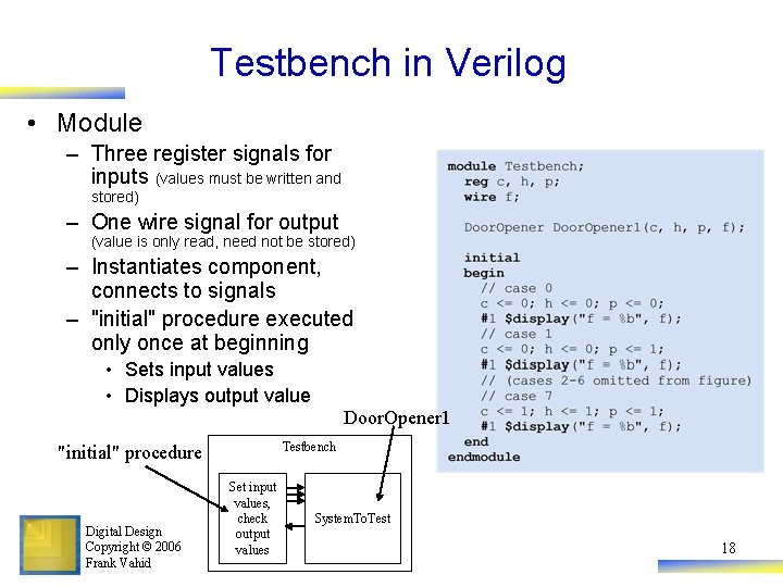
Testbench in Verilog • Module – Three register signals for inputs (values must be written and stored) – One wire signal for output (value is only read, need not be stored) – Instantiates component, connects to signals – "initial" procedure executed only once at beginning • Sets input values • Displays output value Door. Opener 1 Testbench "initial" procedure Digital Design Copyright © 2006 Frank Vahid Set input values, check output values System. To. Test 18

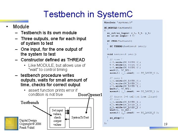
Testbench in System. C • Module – Testbench is its own module – Three outputs, one for each input of system to test – One input, for the one output of the system to test – Constructor defined as THREAD • Like MODULE, but allows use of "wait" to control timing – testbench procedure writes outputs, waits for small amount of time, checks for correct output • assert function prints error if condition is not true Door. Opener 1 Testbench Digital Design Copyright © 2006 Frank Vahid Set input values, check output values System. To. Test 19

Sequential Logic Description using Hardware Description Languages 9. 3 • Will consider description of three sequential components – Registers – Oscillators – Controllers si a tap a rtn o co t g Digital Design Copyright © 2006 Frank Vahid 20

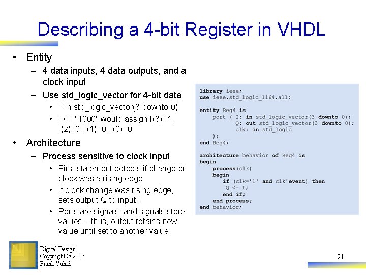
Describing a 4 -bit Register in VHDL • Entity – 4 data inputs, 4 data outputs, and a clock input – Use std_logic_vector for 4 -bit data • I: in std_logic_vector(3 downto 0) • I <= "1000" would assign I(3)=1, I(2)=0, I(1)=0, I(0)=0 • Architecture – Process sensitive to clock input • First statement detects if change on clock was a rising edge • If clock change was rising edge, sets output Q to input I • Ports are signals, and signals store values – thus, output retains new value until set to another value Digital Design Copyright © 2006 Frank Vahid 21

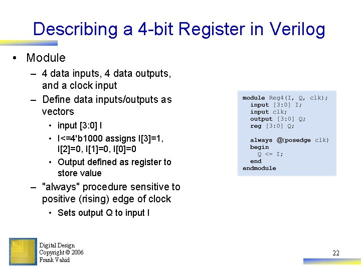
Describing a 4 -bit Register in Verilog • Module – 4 data inputs, 4 data outputs, and a clock input – Define data inputs/outputs as vectors • input [3: 0] I • I<=4'b 1000 assigns I[3]=1, I[2]=0, I[1]=0, I[0]=0 • Output defined as register to store value – "always" procedure sensitive to positive (rising) edge of clock • Sets output Q to input I Digital Design Copyright © 2006 Frank Vahid 22

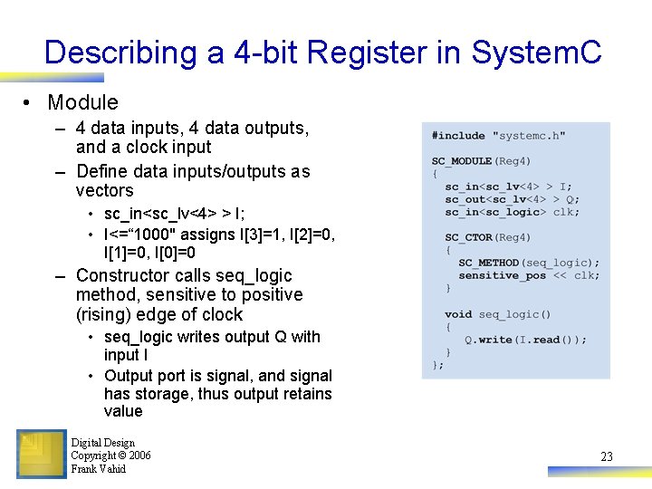
Describing a 4 -bit Register in System. C • Module – 4 data inputs, 4 data outputs, and a clock input – Define data inputs/outputs as vectors • sc_in<sc_lv<4> > I; • I<=“ 1000" assigns I[3]=1, I[2]=0, I[1]=0, I[0]=0 – Constructor calls seq_logic method, sensitive to positive (rising) edge of clock • seq_logic writes output Q with input I • Output port is signal, and signal has storage, thus output retains value Digital Design Copyright © 2006 Frank Vahid 23

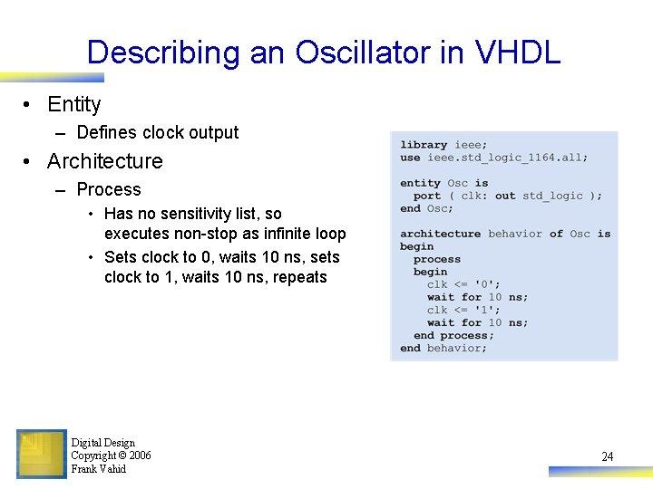
Describing an Oscillator in VHDL • Entity – Defines clock output • Architecture – Process • Has no sensitivity list, so executes non-stop as infinite loop • Sets clock to 0, waits 10 ns, sets clock to 1, waits 10 ns, repeats Digital Design Copyright © 2006 Frank Vahid 24

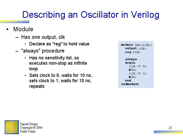
Describing an Oscillator in Verilog • Module – Has one output, clk • Declare as "reg" to hold value – "always" procedure • Has no sensitivity list, so executes non-stop as infinite loop • Sets clock to 0, waits for 10 ns, sets clock to 1, waits for 10 ns, repeats Digital Design Copyright © 2006 Frank Vahid module Osc(clk); output clk; reg clk; always begin clk <= 0; #10; clk <= 1; #10; endmodule 25

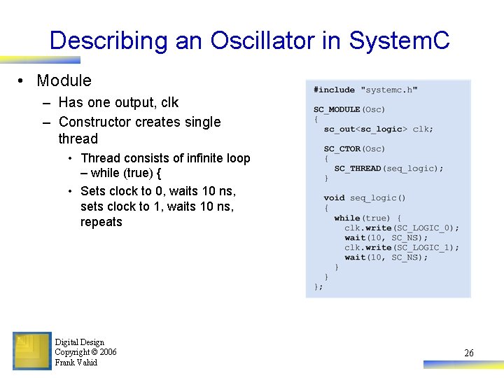
Describing an Oscillator in System. C • Module – Has one output, clk – Constructor creates single thread • Thread consists of infinite loop – while (true) { • Sets clock to 0, waits 10 ns, sets clock to 1, waits 10 ns, repeats Digital Design Copyright © 2006 Frank Vahid 26

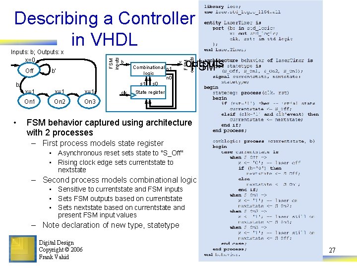
Describing a Controller in VHDL b • b’ x=1 x=1 On 2 On 3 b clk Combinational n 1 logic n 0 s 1 s 0 x outputs FSM outputs Off FSM inputs Inputs: b; Outputs: x x=0 State register FSM behavior captured using architecture with 2 processes – First process models state register • Asynchronous reset sets state to "S_Off" • Rising clock edge sets currentstate to nextstate – Second process models combinational logic • Sensitive to currentstate and FSM inputs • Sets FSM outputs based on currentstate • Sets nextstate based on currentstate and present FSM input values – Note declaration of new type, statetype Digital Design Copyright © 2006 Frank Vahid 27

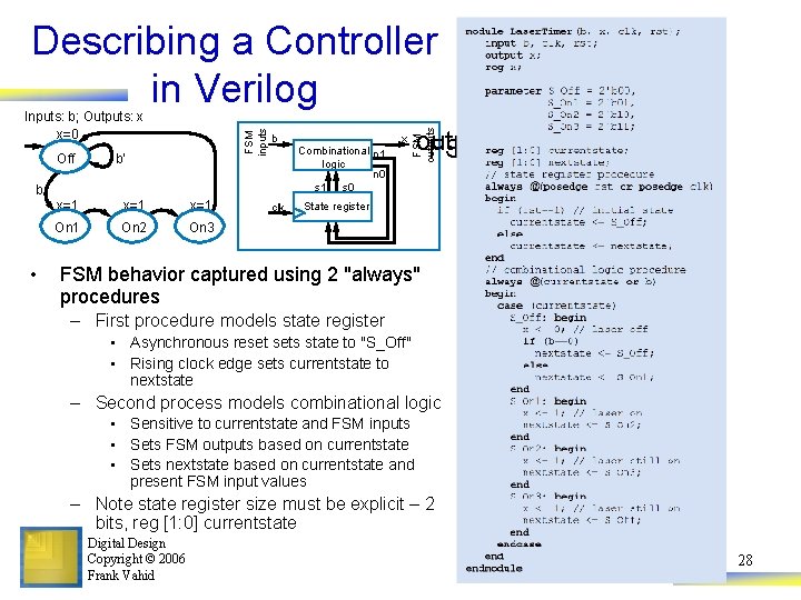
Describing a Controller in Verilog b • b’ x=1 x=1 On 2 On 3 b clk Combinational n 1 logic n 0 s 1 s 0 x outputs FSM outputs Off FSM inputs Inputs: b; Outputs: x x=0 State register FSM behavior captured using 2 "always" procedures – First procedure models state register • Asynchronous reset sets state to "S_Off" • Rising clock edge sets currentstate to nextstate – Second process models combinational logic • Sensitive to currentstate and FSM inputs • Sets FSM outputs based on currentstate • Sets nextstate based on currentstate and present FSM input values – Note state register size must be explicit – 2 bits, reg [1: 0] currentstate Digital Design Copyright © 2006 Frank Vahid 28

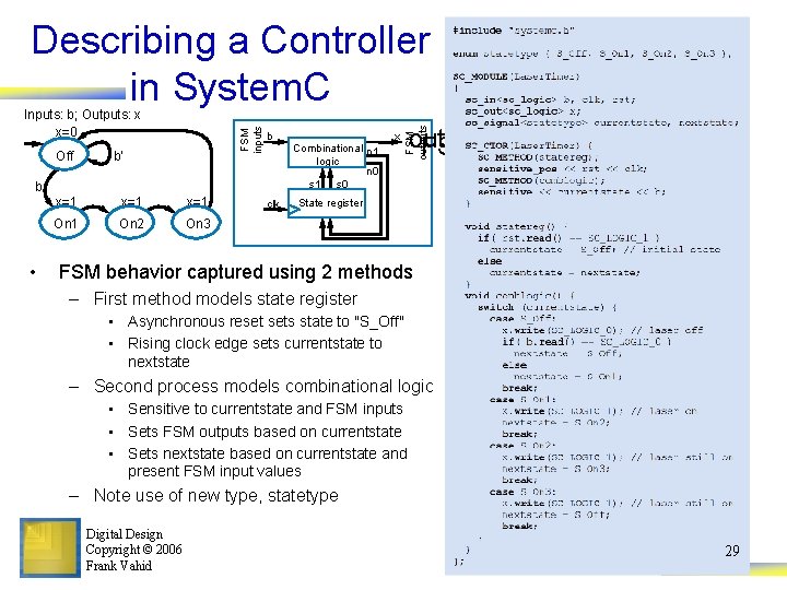
Describing a Controller in System. C b • b’ x=1 x=1 On 2 On 3 b clk Combinational n 1 logic n 0 s 1 s 0 x outputs FSM outputs Off FSM inputs Inputs: b; Outputs: x x=0 State register FSM behavior captured using 2 methods – First method models state register • Asynchronous reset sets state to "S_Off" • Rising clock edge sets currentstate to nextstate – Second process models combinational logic • Sensitive to currentstate and FSM inputs • Sets FSM outputs based on currentstate • Sets nextstate based on currentstate and present FSM input values – Note use of new type, statetype Digital Design Copyright © 2006 Frank Vahid 29

Datapath Component Description using Hardware Description Languages 9. 4 • Will consider description of three datapath components – Full-adders – Carry-ripple adders – Up-counter si a tap a rtn o co t g Digital Design Copyright © 2006 Frank Vahid 30

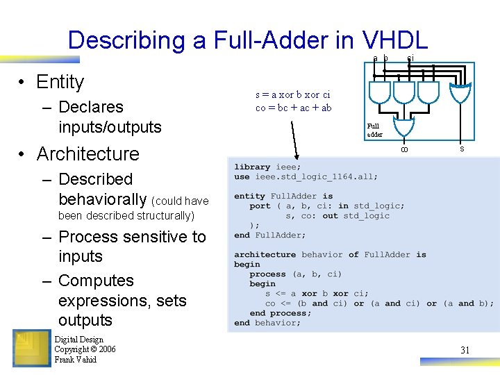
Describing a Full-Adder in VHDL a b • Entity – Declares inputs/outputs • Architecture ci s = a xor b xor ci co = bc + ab Full adder co s – Described behaviorally (could have been described structurally) – Process sensitive to inputs – Computes expressions, sets outputs Digital Design Copyright © 2006 Frank Vahid 31

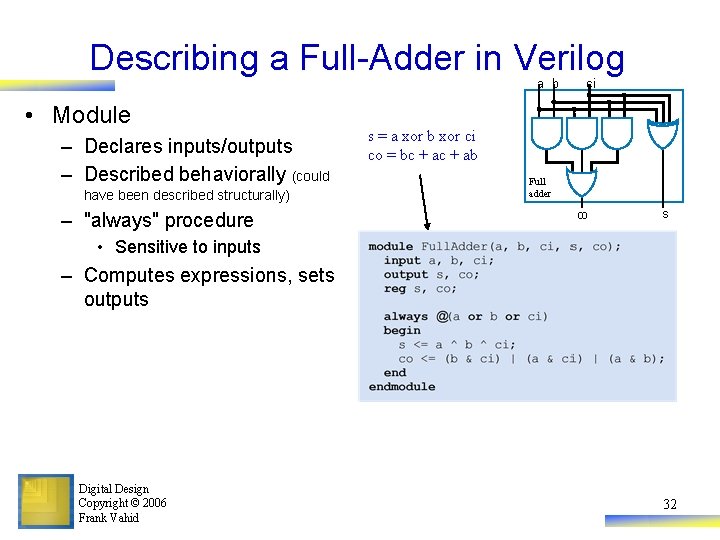
Describing a Full-Adder in Verilog a b • Module – Declares inputs/outputs – Described behaviorally (could have been described structurally) – "always" procedure ci s = a xor b xor ci co = bc + ab Full adder co s • Sensitive to inputs – Computes expressions, sets outputs Digital Design Copyright © 2006 Frank Vahid 32

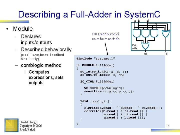
Describing a Full-Adder in System. C a b • Module – Declares inputs/outputs – Described behaviorally (could have been described structurally) – comblogic method • Computes expressions, sets outputs Digital Design Copyright © 2006 Frank Vahid ci s = a xor b xor ci co = bc + ab Full adder co s #include "systemc. h" SC_MODULE(Full. Adder) { sc_in<sc_logic> a, b, ci; sc_out<sc_logic> s, co; SC_CTOR(Full. Adder) { SC_METHOD(comblogic); sensitive << a << b << ci; } void comblogic() { s. write(a. read() ^ co. write((b. read() (a. read() } }; b. read() ^ ci. read()); & ci. read()) | & b. read())); 33

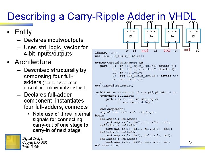
Describing a Carry-Ripple Adder in VHDL • Entity – Declares inputs/outputs – Uses std_logic_vector for 4 -bit inputs/outputs a 3 b 3 a 2 b 2 a 1 b 1 a 0 b 0 ci a b ci FA FA co s 3 co co 3 s s 2 co co 2 s s 1 co co 1 • Architecture – Described structurally by composing four fulladders (could have been described behaviorally instead) – Declares full-adder component, instantiates four full-adders, connects • Note use of three internal signals for connecting carry-out of one stage to carry-in of next stage Digital Design Copyright © 2006 Frank Vahid 34 s s 0

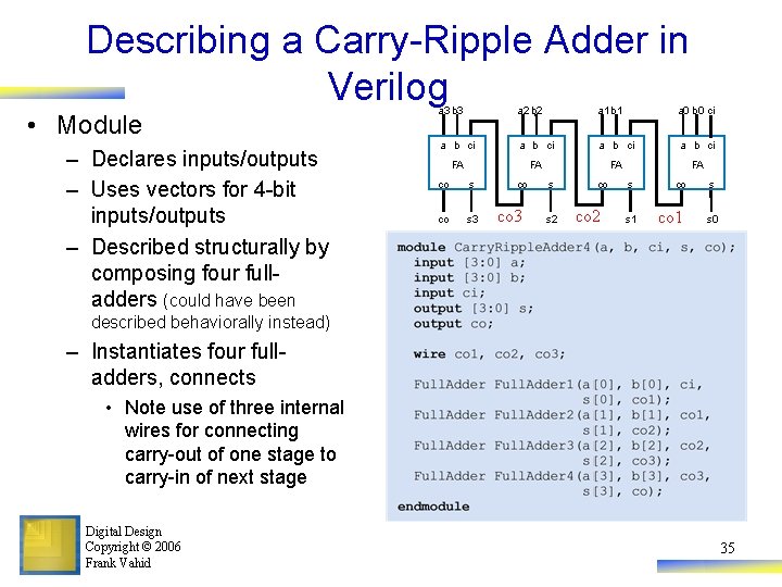
Describing a Carry-Ripple Adder in Verilog • Module – Declares inputs/outputs – Uses vectors for 4 -bit inputs/outputs – Described structurally by composing four fulladders (could have been a 3 b 3 a 2 b 2 a 1 b 1 a 0 b 0 ci a b ci FA FA co s 3 co co 3 s s 2 co co 2 s s 1 co co 1 s s 0 described behaviorally instead) – Instantiates four fulladders, connects • Note use of three internal wires for connecting carry-out of one stage to carry-in of next stage Digital Design Copyright © 2006 Frank Vahid 35

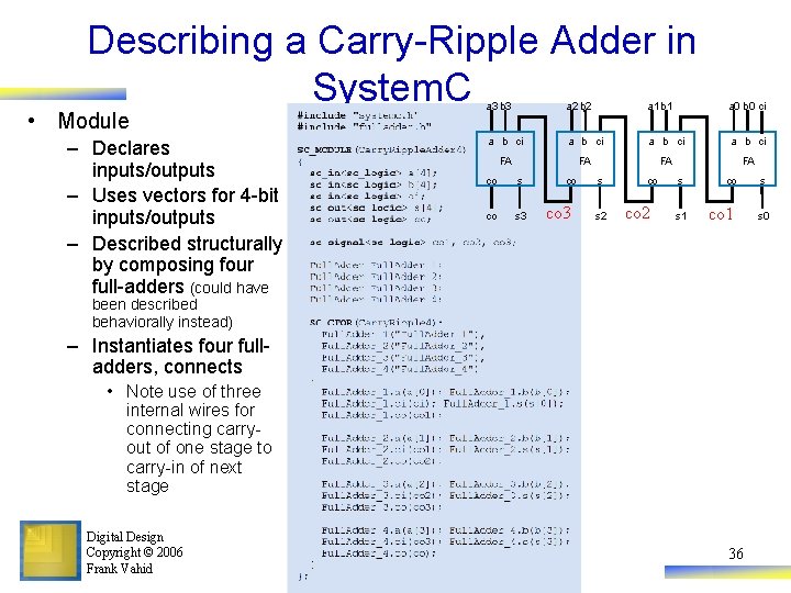
Describing a Carry-Ripple Adder in System. C • Module – Declares inputs/outputs – Uses vectors for 4 -bit inputs/outputs – Described structurally by composing four full-adders (could have a 3 b 3 a 2 b 2 a 1 b 1 a 0 b 0 ci a b ci FA FA co s 3 co co 3 s s 2 co co 2 s s 1 co co 1 been described behaviorally instead) – Instantiates four fulladders, connects • Note use of three internal wires for connecting carryout of one stage to carry-in of next stage Digital Design Copyright © 2006 Frank Vahid 36 s s 0

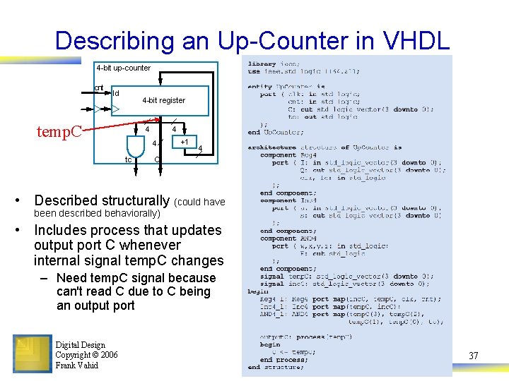
Describing an Up-Counter in VHDL 4 -bit up-counter cnt ld 4 -bit register temp. C 4 4 4 tc +1 4 C • Described structurally (could have been described behaviorally) • Includes process that updates output port C whenever internal signal temp. C changes – Need temp. C signal because can't read C due to C being an output port Digital Design Copyright © 2006 Frank Vahid 37

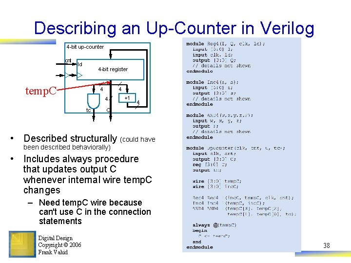
Describing an Up-Counter in Verilog 4 -bit up-counter cnt ld 4 -bit register temp. C 4 4 4 tc +1 4 C • Described structurally (could have been described behaviorally) • Includes always procedure that updates output C whenever internal wire temp. C changes – Need temp. C wire because can't use C in the connection statements Digital Design Copyright © 2006 Frank Vahid 38

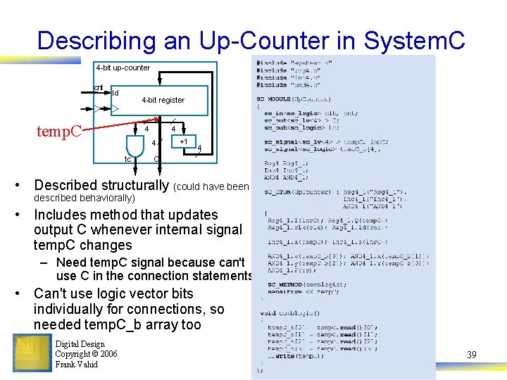
Describing an Up-Counter in System. C 4 -bit up-counter cnt ld 4 -bit register temp. C 4 4 4 tc +1 4 C • Described structurally (could have been described behaviorally) • Includes method that updates output C whenever internal signal temp. C changes – Need temp. C signal because can't use C in the connection statements • Can't use logic vector bits individually for connections, so needed temp. C_b array too Digital Design Copyright © 2006 Frank Vahid 39

RTL Design using Hardware Description Languages 9. 5 • Will consider two forms of RTL descriptions – High-level state machine – Controller and datapath si a tap a rtn o co t g Digital Design Copyright © 2006 Frank Vahid 40

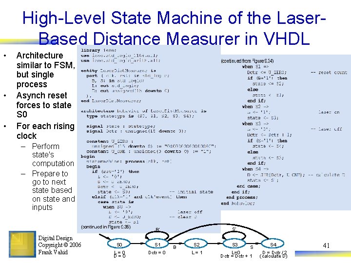
High-Level State Machine of the Laser. Based Distance Measurer in VHDL • • • Architecture similar to FSM, but single process Asynch reset forces to state S 0 For each rising clock – Perform state's computation – Prepare to go to next state based on state and inputs S’ B’ Digital Design Copyright © 2006 Frank Vahid S 0 S 1 L=0 Dctr = 0 B S 2 L=1 S 3 S L=0 Dctr = Dctr + 1 S 4 D = Dctr / 2 (calculate D) 41

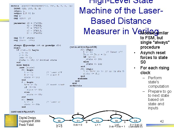
High-Level State Machine of the Laser. Based Distance Measurer in Verilog • Module similar • • to FSM, but single "always" procedure Asynch reset forces to state S 0 For each rising clock – Perform state's computation – Prepare to go to next state based on state and inputs S’ B’ Digital Design Copyright © 2006 Frank Vahid S 0 S 1 L=0 Dctr = 0 B S 2 L=1 S 3 S L=0 Dctr = Dctr + 1 S 4 D = Dctr / 2 (calculate D) 42

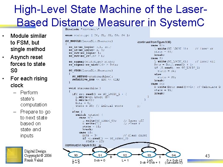
High-Level State Machine of the Laser. Based Distance Measurer in System. C • • • Module similar to FSM, but single method Asynch reset forces to state S 0 For each rising clock – Perform state's computation – Prepare to go to next state based on state and inputs S’ B’ Digital Design Copyright © 2006 Frank Vahid S 0 S 1 L=0 Dctr = 0 B S 2 L=1 S 3 S L=0 Dctr = Dctr + 1 S 4 D = Dctr / 2 (calculate D) 43

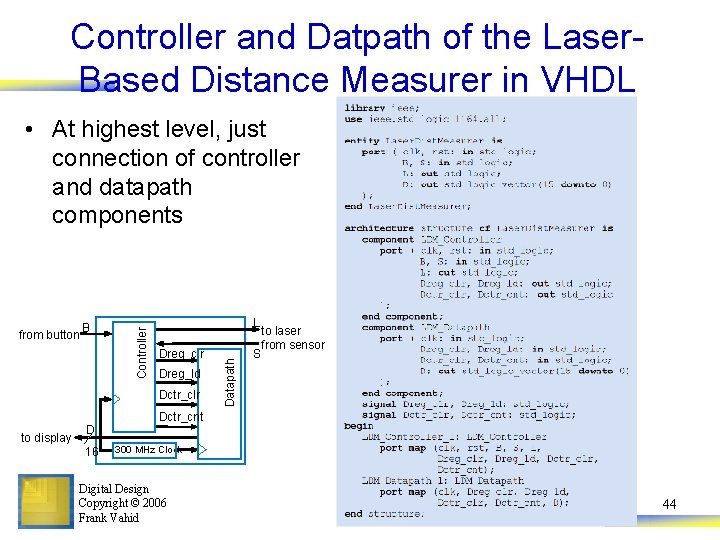
Controller and Datpath of the Laser. Based Distance Measurer in VHDL B L Dreg_clr Dreg_ld Dctr_clr to display D 16 Datapath from button Controller • At highest level, just connection of controller and datapath components S to laser from sensor Dctr_cnt 300 MHz Clock Digital Design Copyright © 2006 Frank Vahid 44

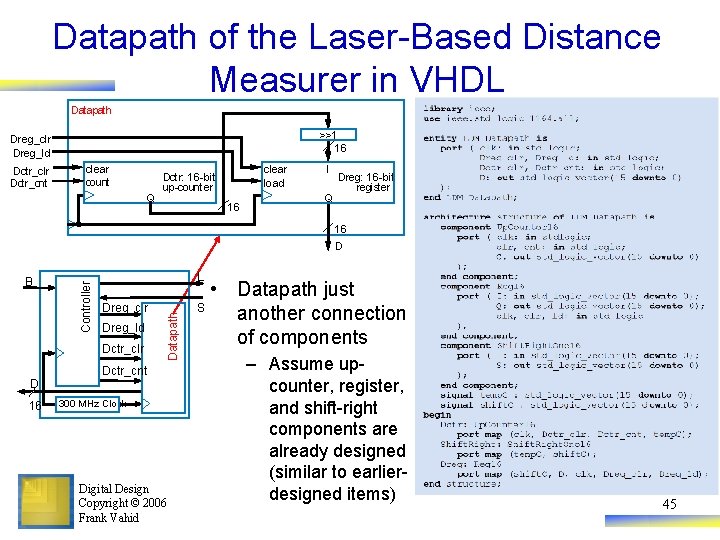
Datapath of the Laser-Based Distance Measurer in VHDL Datapath >>1 16 Dreg_clr Dreg_ld Dctr_clr Dctr_cnt clear count Q clear load Dctr: 16 -bit up-counter 16 I Q Dreg: 16 -bit register 16 L Dreg_clr Dreg_ld Dctr_clr D 16 Datapath B Controller D Dctr_cnt 300 MHz Clock Digital Design Copyright © 2006 Frank Vahid S • Datapath just another connection of components – Assume upcounter, register, and shift-right components are already designed (similar to earlierdesigned items) 45

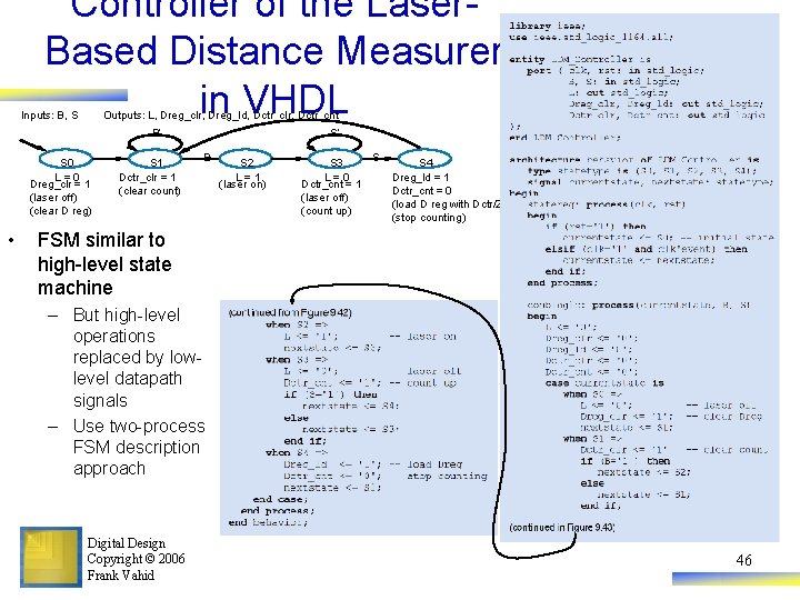
Controller of the Laser. Based Distance Measurer in VHDL Inputs: B, S Outputs: L, Dreg_clr, Dreg_ld, Dctr_clr, Dctr_cnt B’ S 0 L=0 Dreg_clr = 1 (laser off) (clear D reg) • S 1 Dctr_clr = 1 (clear count) S’ B S 2 L=1 (laser on) S S 3 L=0 Dctr_cnt = 1 (laser off) (count up) S 4 Dreg_ld = 1 Dctr_cnt = 0 (load D reg with Dctr/2) (stop counting) FSM similar to high-level state machine – But high-level operations replaced by lowlevel datapath signals – Use two-process FSM description approach Digital Design Copyright © 2006 Frank Vahid 46

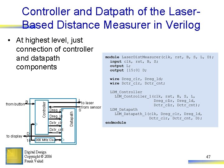
Controller and Datpath of the Laser. Based Distance Measurer in Verilog B L Dreg_clr Dreg_ld Dctr_clr to display D 16 Datapath from button Controller • At highest level, just connection of controller and datapath components S to laser from sensor Dctr_cnt 300 MHz Clock Digital Design Copyright © 2006 Frank Vahid 47

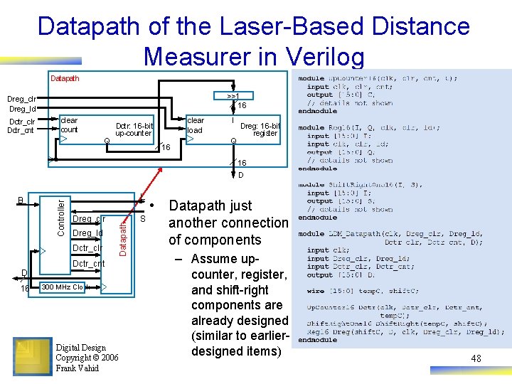
Datapath of the Laser-Based Distance Measurer in Verilog Datapath >>1 16 Dreg_clr Dreg_ld Dctr_clr Dctr_cnt clear count Q clear load Dctr: 16 -bit up-counter 16 I Q Dreg: 16 -bit register 16 L Dreg_clr Dreg_ld Dctr_clr D 16 Datapath B Controller D Dctr_cnt 300 MHz Clock Digital Design Copyright © 2006 Frank Vahid S • Datapath just another connection of components – Assume upcounter, register, and shift-right components are already designed (similar to earlierdesigned items) 48

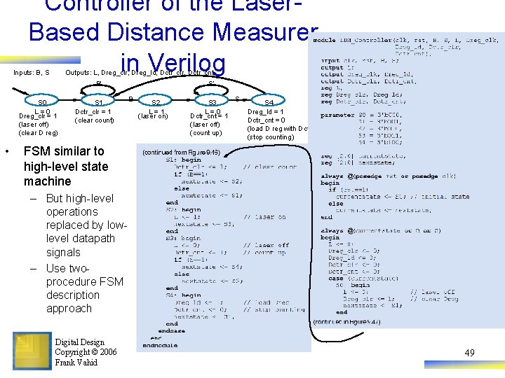
Controller of the Laser. Based Distance Measurer in Verilog Inputs: B, S Outputs: L, Dreg_clr, Dreg_ld, Dctr_clr, Dctr_cnt B’ S 0 L=0 Dreg_clr = 1 (laser off) (clear D reg) • S 1 Dctr_clr = 1 (clear count) S’ B S 2 L=1 (laser on) S S 3 L=0 Dctr_cnt = 1 (laser off) (count up) S 4 Dreg_ld = 1 Dctr_cnt = 0 (load D reg with Dctr/2) (stop counting) FSM similar to high-level state machine – But high-level operations replaced by lowlevel datapath signals – Use twoprocedure FSM description approach Digital Design Copyright © 2006 Frank Vahid 49

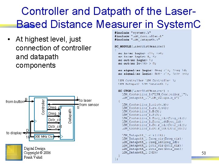
Controller and Datpath of the Laser. Based Distance Measurer in System. C B L Dreg_clr Dreg_ld Dctr_clr to display D 16 Datapath from button Controller • At highest level, just connection of controller and datapath components S to laser from sensor Dctr_cnt 300 MHz Clock Digital Design Copyright © 2006 Frank Vahid 50

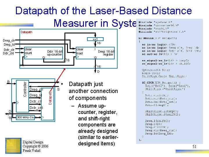
Datapath of the Laser-Based Distance Measurer in System. C Datapath >>1 16 Dreg_clr Dreg_ld Dctr_clr Dctr_cnt clear count Q clear load Dctr: 16 -bit up-counter 16 I Q Dreg: 16 -bit register 16 L Dreg_clr Dreg_ld Dctr_clr D 16 Datapath B Controller D Dctr_cnt 300 MHz Clock Digital Design Copyright © 2006 Frank Vahid S • Datapath just another connection of components – Assume upcounter, register, and shift-right components are already designed (similar to earlierdesigned items) 51

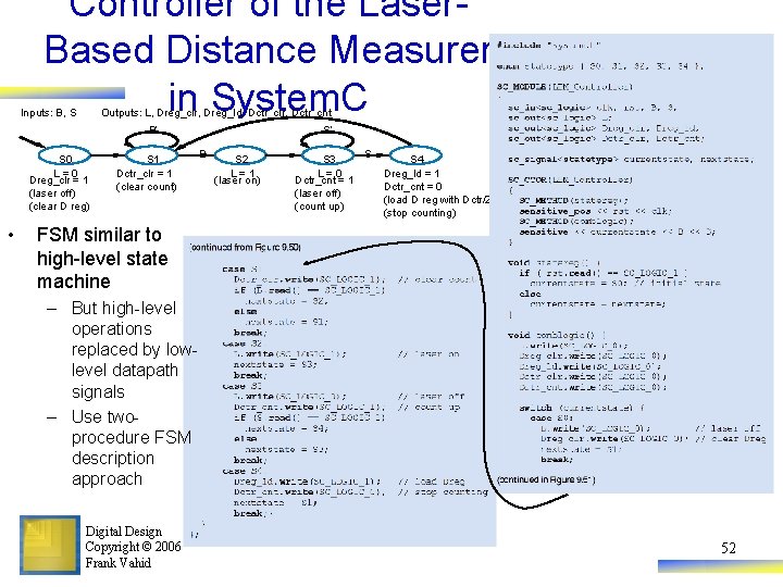
Controller of the Laser. Based Distance Measurer in System. C Inputs: B, S Outputs: L, Dreg_clr, Dreg_ld, Dctr_clr, Dctr_cnt B’ S 0 L=0 Dreg_clr = 1 (laser off) (clear D reg) • S 1 Dctr_clr = 1 (clear count) S’ B S 2 L=1 (laser on) S S 3 L=0 Dctr_cnt = 1 (laser off) (count up) S 4 Dreg_ld = 1 Dctr_cnt = 0 (load D reg with Dctr/2) (stop counting) FSM similar to high-level state machine – But high-level operations replaced by lowlevel datapath signals – Use twoprocedure FSM description approach Digital Design Copyright © 2006 Frank Vahid 52

Chapter Summary • Hardware Description Languages (HDLs) are widely used in modern digital design – Textual rather than graphical language sufficient for many purposes – HDLs are computer-readable – Great for simulation • VHDL, Verilog, and System. C are popular • Introduced languages mainly through examples • Numerous HDL books exist to teach language in more detail Digital Design Copyright © 2006 Frank Vahid 53