Chapter 6 FPGA Modules and Hardware Interface Design


 u The algorithm used for the calculation")
 u The 1 D IDCT coefficients for")


 u The output Y of an 8‧ 8 IDCT")
 Z(0, 0) = 23170 x 00 + 32138 x")


 u What is AMBA? n The Advanced Microcontroller Bus Architecture")
 u Objectives of the AMBA specification. n To facilitate the")
 u Typical AMBA system. High-performance ARM-processor High-bandwidth External Memory Interface")
 u Feature AMBA AHB AMBA ASB AMBA APB Feature")
 u When to use AMBA AHB/ASB or APB. n A")


![6. 2 AMBA AHB Transfer Type u Transfer type encoding. n HTRANS[1: 0] l](https://slidetodoc.com/presentation_image_h/904ce6dd98a7ac2d21f32c4433e9a788/image-23.jpg "6. 2 AMBA AHB Transfer Type u Transfer type encoding. n HTRANS[1: 0] l")
![6. 2 Slave Transfer Responses u Response encoding. n HRESP[1: 0] l 00 –](https://slidetodoc.com/presentation_image_h/904ce6dd98a7ac2d21f32c4433e9a788/image-24.jpg "6. 2 Slave Transfer Responses u Response encoding. n HRESP[1: 0] l 00 –")


. High-performance ARM-processor")


 u The strobe control method employs a single control")
 u Source-initiated strobe for data transfer. Source unit Data")
 u Destination-initiated strobe for data transfer. Data bus Source")


 u Data transfer procedure initiated by the")
 u Data transfer procedure initiated by the")


 CPU BG BR RD WR Address")

- Slides: 71
Chapter 6 FPGA Modules and Hardware Interface Design Professor Tzyy-Kuen Tien E-mail: tktien@mail. stut. edu. tw Http: //www. eecs. stut. edu. tw STUT/EE
Outline 6. 1 The Implementation of IDCT on FPGA 6. 2 AMBA I/O Interface Design 6. 3 I/O Interface Design 教育部顧問室PAL聯盟/系統雛型與軟硬體整合設計 第六章:FPGA模組與硬體介面設計 P-2/93
6. 1 The Implementation of IDCT on FPGA 6. 2 AMBA I/O Interface Design 6. 3 I/O Interface Design 教育部顧問室PAL聯盟/系統雛型與軟硬體整合設計 第六章:FPGA模組與硬體介面設計 P-3/93
6. 1 Compression/Decompression System u A block diagram of a compression/decompression system. u DCT/IDCT can be used in the system to reduce the bandwidth requirements. 教育部顧問室PAL聯盟/系統雛型與軟硬體整合設計 第六章:FPGA模組與硬體介面設計 P-4/93
6. 1 Introduction to IDCT u Inverse Discrete Cosine Transform. u IDCT is used to decompress DCT compressed data in the decoder. u IDCT is one of the most computation-intensive parts of the MPEG decoding process. u A fast, hardware based IDCT implementation is crucial to speed the MPEG decoding process. 教育部顧問室PAL聯盟/系統雛型與軟硬體整合設計 第六章:FPGA模組與硬體介面設計 P-5/93
6. 1 2 D IDCT Equations (1/2) u The algorithm used for the calculation of the 2 D IDCT coefficients is based on the following equation: M-1 XCpq = ∑ m=0 N-1 c(p)c(q) ∑ XNmn · 4 n=0 ·cos Π(2 m+1)p 2 M ·cos Π(2 n+1)q 2 N (EQ 1) u First, the 1 D DCT of the rows are calculated and then the 1 D IDCT of the columns are calculated. 教育部顧問室PAL聯盟/系統雛型與軟硬體整合設計 第六章:FPGA模組與硬體介面設計 P-6/93
6. 1 2 D IDCT Equations (2/2) u The 1 D IDCT coefficients for the rows and columns can be calculated by separating equation 1 into the row part and the column part. C = K · cos K= Ct √ 1 N = K · cos K= √ 1 M (2·col number + 1) · row number ·Π (EQ 2) 2·M for row = 0, K= √ 2 N for row ≠ 0 (2·row number + 1) · col number ·Π (EQ 3) 2·N for col = 0, K= √ 2 M for col ≠ 0 M = total number of columns, N = total number of rows. 教育部顧問室PAL聯盟/系統雛型與軟硬體整合設計 第六章:FPGA模組與硬體介面設計 P-7/93
6. 1 Constant Values of C and Ct u The constant values for C and Ct calculated from equations 2 and 3 are as follows: C= Ct = 23170 32138 27246 18205 30274 12540 – 12540 27246 – 6393 – 32138 23170 – 23170 18205 – 32138 6393 12540 – 30274 6393 – 18205 27246 23170 6393 – 18205 – 27246 – 30274 – 12540 – 18205 32138 6393 23170 – 23170 27246 – 6393 32138 – 12540 30274 – 32138 – 27246 18205 23170 – 32138 30274 – 27246 23170 – 18205 12540 – 6393 23170 32138 30274 27246 23170 18205 12540 6393 23170 27246 12540 – 6393 – 23170 – 32138 – 30274 – 18205 23170 18205 – 12540 – 32138 – 23170 6393 30274 27246 23170 6393 – 30274 – 18205 23170 27246 – 12540 – 32138 23170 – 6393 – 30274 18205 23170 – 27246 – 12540 32138 23170 – 18205 – 12540 32138 – 23170 – 6393 30274 – 27246 23170 – 27246 12540 6393 – 23170 32138 – 30274 18205 23170 – 32138 30274 – 27246 23170 – 18205 12540 – 6393 教育部顧問室PAL聯盟/系統雛型與軟硬體整合設計 第六章:FPGA模組與硬體介面設計 P-8/93
6. 1 2 D IDCT using Vector Processing u A one-dimensional 8 -point IDCT followed by an internal double buffer memory, followed by another one-dimensional 8 -point IDCT provides the 2 D IDCT architecture. 1 D IDCT RAM Double Buffer 1 D IDCT u Vector processing using parallel multipliers is a method used for implementation of IDCT. u Advantages of vector processing method. n Regular structure, simple control and interconnect, good balance between performance and complexity of implementation. 教育部顧問室PAL聯盟/系統雛型與軟硬體整合設計 第六章:FPGA模組與硬體介面設計 P-9/93
6. 1 Behavioral Model (1/2) u The output Y of an 8‧ 8 IDCT for input X is given by Y = C‧X‧Ct, where C is the cosine coefficients and Ct is the transpose coefficients. u The equation can also be written as Y = Ct‧Z, where Z = X‧C. X= x 00 x 01 x 02 x 03 x 04 x 05 x 06 x 07 x 10 x 11 x 12 x 13 x 14 x 15 x 16 x 17 x 20 x 21 x 22 x 23 x 24 x 25 x 26 x 27 x 30 x 31 x 32 x 33 x 34 x 35 x 36 x 37 x 40 x 41 x 42 x 43 x 44 x 45 x 46 x 47 x 50 x 51 x 52 x 53 x 54 x 55 x 56 x 57 x 60 x 61 x 62 x 63 x 64 x 65 x 66 x 67 x 70 x 71 x 72 x 73 x 74 x 75 x 76 x 77 教育部顧問室PAL聯盟/系統雛型與軟硬體整合設計 23170 23170 32138 27246 18205 6393 – 18205 – 27246 30274 12540 – 30274 – 12540 C = 27246 – 6393 – 32138 – 18205 32138 6393 23170 – 23170 18205 – 32138 6393 27246 – 6393 32138 12540 – 30274 – 12540 30274 – 30274 6393 – 18205 27246 – 32138 – 27246 18205 第六章:FPGA模組與硬體介面設計 23170 – 32138 30274 – 27246 23170 – 18205 12540 – 6393 P-10/93
6. 1 Behavioral Model (2/2) Z(0, 0) = 23170 x 00 + 32138 x 01 + 30274 x 02 + 27246 x 03 + 23170 x 04 + 18205 x 05 + 12540 x 06 + 6393 x 07 Z(0, 1) = 23170 x 00 + 27246 x 01 + 12540 x 02 – 6393 x 03 – 23170 x 04 – 3213805 – 30274 x 06 – 18205 x 07 Z(0, 2) = 23170 x 00 + 18205 x 01 – 12540 x 02 – 32138 x 03 – 23170 x 04 + 6393 x 05 + 30274 x 06 + 27246 x 07 Z(0, 3) = 23170 x 00 + 6393 x 01 – 30274 x 02 – 18205 x 03 + 23170 x 04 + 27246 x 05 – 12540 x 06 – 3213807 Z(0, 4) = 23170 x 00 – 6393 x 01 – 30274 x 02 + 18205 x 03 + 23170 x 04 – 27246 x 05 – 12540 x 06 + 32138 x 07 Z(0, 5) = 23170 x 00 – 18205 x 01 – 12540 x 02 + 32138 x 03 – 23170 x 04 – 6393 x 05 + 30274 x 06 – 27246 x 07 Z(0, 6) = 23170 x 00 – 27246 x 01 + 12540 x 02 + 6393 x 03 – 23170 x 04 + 32138 x 05 – 30274 x 06 + 18205 x 07 Z(0, 7) = 23170 x 00 – 32138 x 01 + 30274 x 02 – 27246 x 03 + 23170 x 04 – 18205 x 05 + 12540 x 06 – 6393 x 07 Or: Z(k, 0) = (23170 xk 0 + 30274 xk 2 + 23170 xk 4 + 12540 xk 6) + (32138 xk 1 + 27246 xk 3 + 18205 xk 5 + 6393 xk 7) = P 01 + P 02 Z(k, 1) = (23170 xk 0 + 12540 xk 2 – 23170 xk 4 – 30274 xk 6) + (27246 xk 1 – 6393 xk 3 – 32138 xk 5 – 18205 xk 7) = P 11 + P 12 Z(k, 2) = (23170 xk 0 – 12540 xk 2 – 23170 xk 4 + 30274 xk 6) + (18205 xk 1 – 32138 xk 3 + 6393 xk 5 + 27246 xk 7) = P 21 + P 22 Z(k, 3) = (23170 xk 0 – 30274 xk 2 + 23170 xk 4 – 12540 xk 6) + (6393 xk 1 – 18205 xk 3 + 27246 xk 5 – 32138 xk 7) = P 31 + P 32 Z(k, 4) = P 31 – P 32 Z(k, 5) = P 21 – P 22 Z(k, 6) = P 11 – P 12 Z(k, 7) = P 01 – P 02 where k = 0, 2, …, 7 教育部顧問室PAL聯盟/系統雛型與軟硬體整合設計 第六章:FPGA模組與硬體介面設計 P-11/93
6. 1 1 D IDCT u The block diagram for the implementation of the 1 D IDCT is shown below. 教育部顧問室PAL聯盟/系統雛型與軟硬體整合設計 第六章:FPGA模組與硬體介面設計 P-12/93
6. 2 AMBA I/O Interface Design 6. 1 The Implementation of IDCT on FPGA 6. 2 AMBA I/O Interface Design 6. 3 I/O Interface Design 教育部顧問室PAL聯盟/系統雛型與軟硬體整合設計 第六章:FPGA模組與硬體介面設計 P-13/93
6. 2 AMBA I/O Interface Design u Introduction to the AMBA buses u AMBA AHB bus u AMBA ASB bus u AMBA APB bus 教育部顧問室PAL聯盟/系統雛型與軟硬體整合設計 第六章:FPGA模組與硬體介面設計 P-14/93
6. 2 Introduction (1/5) u What is AMBA? n The Advanced Microcontroller Bus Architecture specification. n An on-chip communication standard for designing highperformance embedded microcontroller. u Three distinct buses. n AHB (the Advanced High-performance Bus). l High-performance system backbone bus. n ASB (the Advanced System Bus). l An alternative system bus. n APB (the Advanced Peripheral Bus). l Minimal power consumption. l Reduced interface complexity. 教育部顧問室PAL聯盟/系統雛型與軟硬體整合設計 第六章:FPGA模組與硬體介面設計 P-15/93
6. 2 Introduction (2/5) u Objectives of the AMBA specification. n To facilitate the right-first-time development of embedded microcontroller products. n To be technology-independent. n To ensure that highly reusable peripheral and system. macrocells can be migrated across a diverse range of IC processes. n To encourage modular system design. n To minimize the silicon infrastructure required for both operation and manufacturing test. 教育部顧問室PAL聯盟/系統雛型與軟硬體整合設計 第六章:FPGA模組與硬體介面設計 P-16/93
6. 2 Introduction (3/5) u Typical AMBA system. High-performance ARM-processor High-bandwidth External Memory Interface High-bandwidth On-chip RAM AHB or ASB DMA bus master B R I D G E UART Timer APB Keypad PIO AHB to APB Bridge Or ASB to APB Bridge 教育部顧問室PAL聯盟/系統雛型與軟硬體整合設計 第六章:FPGA模組與硬體介面設計 P-17/93
6. 2 Introduction (4/5) u Feature AMBA AHB AMBA ASB AMBA APB Feature High performance Low power Pipelined operation Latched address and control Multiple bus masters Simple interface Burst transfers Suitable for many peripherals Split transactions Dual-clock edge operation Single-clock edge operation (rising edge) Single-cycle bus master handover Single-clock edge operation (rising edge) Wider data bus configuration Components AHB master ASB master APB bridge (slave on AHB or ASB) AHB slave ASB slave APB slave AHB arbiter ASB arbiter AHB decoder ASB decoder 教育部顧問室PAL聯盟/系統雛型與軟硬體整合設計 第六章:FPGA模組與硬體介面設計 P-18/93
6. 2 Introduction (5/5) u When to use AMBA AHB/ASB or APB. n A full AHB or ASB. l Bus masters. l On-chip memory blocks. l External memory interface. l High-bandwidth peripherals with FIFO interfaces. l DMA slave peripherals. n A simple APB interface. l Simple register-mapped slave devices. l Very low power interfaces where clocks cannot be globally routed. l Grouping narrow-bus peripherals to avoid loading the system bus. 教育部顧問室PAL聯盟/系統雛型與軟硬體整合設計 第六章:FPGA模組與硬體介面設計 P-19/93
6. 2 AMBA I/O Interface Design u Introduction to the AMBA buses u AMBA AHB bus u AMBA ASB bus u AMBA APB bus 教育部顧問室PAL聯盟/系統雛型與軟硬體整合設計 第六章:FPGA模組與硬體介面設計 P-20/93
6. 2 A Typical AHB and APB System High-performance ARM-processor High-bandwidth on-chip RAM B R I D G E AHB High-bandwidth Memory Interface DMA bus master UART Timer APB Keypad PIO AHB to APB Bridge AMBA Advanced High-performance Bus (AHB) AMBA Advanced Peripheral Bus (APB) *High performance *Low power *Pipelined operation *Latched address and control *Burst transfers *Simple interface *Multiple bus masters *Suitable for many peripherals *Split transactions 教育部顧問室PAL聯盟/系統雛型與軟硬體整合設計 第六章:FPGA模組與硬體介面設計 P-21/93
6. 2 AMBA AHB Bus Interconnect u Multiplexor interconnection. HADDR HWDATA HADDR HRDATA HWDATA HRDATA HADDR HWDATA Address and control mux HRDATA HADDR HWDATA Write data mux Read data mux HRDATA HADDR HWDATA HRDATA 教育部顧問室PAL聯盟/系統雛型與軟硬體整合設計 第六章:FPGA模組與硬體介面設計 P-22/93
6. 2 AMBA AHB Transfer Type u Transfer type encoding. n HTRANS[1: 0] l 00 – IDLE No data transfer is required. l 01 – BUSY Bus masters insert IDLE cycles in the middle of bursts of transfers. l 10 – NONSEQ The first transfer of a burst or a single transfer is initiated. l 11 – SEQ The remaining transfers are in a burst. The address is related to the previous transfer. 教育部顧問室PAL聯盟/系統雛型與軟硬體整合設計 第六章:FPGA模組與硬體介面設計 P-23/93
6. 2 Slave Transfer Responses u Response encoding. n HRESP[1: 0] l 00 – OKAY. l 01 – ERROR. l 10 – RETRY. The signal shows the transfer has not yet completed, so the bus master should retry the transfer. l 11 – SPLIT The slave will request access to the bus on behalf of the master when the transfer can complete. u If the response is the one among ERROR, RETRY and SPLIT, a two-cycle response is required. 教育部顧問室PAL聯盟/系統雛型與軟硬體整合設計 第六章:FPGA模組與硬體介面設計 P-24/93
6. 2 AMBA AHB Bus Arbitration u Bus master grant signals. n The HGRANTx signal is only used by the master to determine when it owns the bus. HMASTER[3: 0] HGRANT_M 1 Decoder Master HADDR_M 1[31: 0] #1 Arbiter HGRANT_M 2 Master HADDR_M 2[31: 0] HADDR to all slaves #2 Address and Control multiplex HGRANT_M 3 Master HADDR_M 3[31: 0] #3 教育部顧問室PAL聯盟/系統雛型與軟硬體整合設計 第六章:FPGA模組與硬體介面設計 P-25/93
6. 2 AMBA AHB Bus Slave u AHB bus slave interface. Select HSELx HADDR[31: 0] Address and control HWRITE HTRANS[1: 0] HSIZE[2: 0] HBURST[2: 0] Data HWDATA[31: 0] Reset Clock HRESETn HCLK HMASTER[3: 0] HMASTLOCK 教育部顧問室PAL聯盟/系統雛型與軟硬體整合設計 HREADY AHB slave HRESP[1: 0] HRDATA[31: 0] Split-capable slave Transfer response Data HSPLITx[15: 0] 第六章:FPGA模組與硬體介面設計 P-26/93
6. 2 AMBA AHB Bus Master u AHB bus master interface. HBUSREQx Arbiter grant Transfer response HGRANTx HREADY HRESP[1: 0] Reset HRESETn Clock HCLK HLOCKx Arbiter HTRANS[1: 0] Transfer type HADDR[31: 0] AHB master HWRITE HSIZE[2: 0] Address and control HBURST[2: 0] Data HRDATA[31: 0] HPROT[3: 0] HWDATA[31: 0] 教育部顧問室PAL聯盟/系統雛型與軟硬體整合設計 Data 第六章:FPGA模組與硬體介面設計 P-27/93
6. 2 AMBA AHB Arbiter u AHB arbiter interface. HBUSREQx 1 HLOCKx 1 Arbiter requests and locks HBUSREQx 2 HLOCKx 2 HBUSREQx 3 HGRANTx 1 HLOCKx 3 HADDR[31: 0] Address and control HSPLITx[15: 0] HTRANS[1: 0] HBURST[2: 0] HGRANTx 2 AHB arbiter HGRANTx 3 Arbiter grants HMASTER[3: 0] HMASTLOCK HRESP[1: 0] HREADY Reset Clock HRESETn HCLK 教育部顧問室PAL聯盟/系統雛型與軟硬體整合設計 第六章:FPGA模組與硬體介面設計 P-28/93
6. 2 AMBA I/O Interface Design u Introduction to the AMBA buses u AMBA AHB bus u AMBA ASB bus u AMBA APB bus 教育部顧問室PAL聯盟/系統雛型與軟硬體整合設計 第六章:FPGA模組與硬體介面設計 P-29/93
6. 2 A Typical AMBA ASB-based Microcontroller u A typical AMBA system. High-performance ARM-processor High-bandwidth on-chip RAM B R I D G E ASB High-bandwidth Memory Interface DMA bus master UART APB Keypad PIO ASB to APB Bridge AMBA Advanced System Bus (ASB) AMBA Advanced Peripheral Bus (APB) *High performance *Low power *Pipelined operation *Latched address and control *Burst transfers *Simple interface *Multiple bus masters *Suitable for many peripherals 教育部顧問室PAL聯盟/系統雛型與軟硬體整合設計 Timer 第六章:FPGA模組與硬體介面設計 P-30/93
6. 2 AMBA ASB Description u Basic flow of the bus operation. n The arbiter determines which master is granted access to the bus. n When granted, a master initiates transfers on the bus. n The decoder uses the high order address lines to select a bus slave. n The slave provides a transfer response back lines to the bus master and data is transferred between the master and slave. 教育部顧問室PAL聯盟/系統雛型與軟硬體整合設計 第六章:FPGA模組與硬體介面設計 P-31/93
6. 2 ASB Transfers u Three types of transfer. n NONSEQUENTIAL l Used for signal transfers or the first transfer of a burst. n SEQUENTIAL l Used for transfers in a burst. The address of a SEQUENTIAL transfer is always related to the previous transfer. n ADDRESS-ONLY l Used when no data movement is required. 教育部顧問室PAL聯盟/系統雛型與軟硬體整合設計 第六章:FPGA模組與硬體介面設計 P-32/93
6. 2 AMBA ASB Bus Slave u ASB bus slave interface. Select DSEL BA[31: 0] Address and control BWRITE BSIZE[1: 0] Reset Bn. RES Clock BCLK 教育部顧問室PAL聯盟/系統雛型與軟硬體整合設計 BWAIT ASB slave BERROR BLAST BD[31: 0] Transfer response Data 第六章:FPGA模組與硬體介面設計 P-33/93
6. 2 AMBS ASB Bus Master u ASB bus master interface. Arbiter grant AREQ AGNT BWAIT Transfer response BERROR BLAST ASB master BLOK Arbiter BTRAN[1: 0] Transfer type BA[31: 0] BWRITE Reset Bn. RES BSIZE[1: 0] Clock BCLK BPROT[1: 0] BD[31: 0] 教育部顧問室PAL聯盟/系統雛型與軟硬體整合設計 Address and control Data 第六章:FPGA模組與硬體介面設計 P-34/93
6. 2 AMBA ASB Bus Decoder u ASB decoder interface. Transfer type DSEL 1 BTRAN[1: 0] DSEL 1 …. . BA[31: 0] Address and control BWRITE BSIZE[1: 0] BPROT[1: 0] DSELn ASB decoder BWAIT Reset Bn. RES BERROR Clock BCLK BLAST 教育部顧問室PAL聯盟/系統雛型與軟硬體整合設計 Selects Transfer response 第六章:FPGA模組與硬體介面設計 P-35/93
6. 2 AMBA ASB Bus Arbiter u ASB arbiter interface. AREQx 1 AGNTx 1 Arbiter requests AREQx 2 AGNTx 2 AREQx 3 AGNTx 3 Wait BWAIT Lock BLOK Reset Bn. RES Clock BCLK 教育部顧問室PAL聯盟/系統雛型與軟硬體整合設計 Arbiter grants ASB arbiter 第六章:FPGA模組與硬體介面設計 P-36/93
6. 2 AMBA I/O Interface Design u Introduction to the AMBA buses u AMBA AHB bus u AMBA ASB bus u AMBA APB bus 教育部顧問室PAL聯盟/系統雛型與軟硬體整合設計 第六章:FPGA模組與硬體介面設計 P-37/93
6. 2 A Typical AMBA-based Microcontroller u AMBA Advanced Peripheral Bus (APB). High-performance ARM-processor High-bandwidth Memory Interface High-bandwidth on-chip RAM B R I D G E AHB or ASB DMA bus master UART Timer APB Keypad PIO APB Bridge AMBA Advanced Peripheral Bus (APB) *Low power *Latched address and control *Simple interface *Suitable for many peripherals 教育部顧問室PAL聯盟/系統雛型與軟硬體整合設計 第六章:FPGA模組與硬體介面設計 P-38/93
6. 2 Avtivity of the Peripheral Bus u State diagram. n IDLE l The default state for the peripheral bus. n SETUP l The bus moves into this state when a transfer is required. l The bus remains in the SETUP state for one clock and will always move to the ENABLE state. l PSELx is asserted. n ENABLE l PENABLE is asserted. l The address, write and select signals all remain stable during SETUP ENABLE. l Glitch is acceptable during No transfer ENABLE SETUP. 教育部顧問室PAL聯盟/系統雛型與軟硬體整合設計 第六章:FPGA模組與硬體介面設計 No transfer Transfer P-39/93
6. 2 AMBA APB Interface Design u APB bridge interface. PSEL 1 PSEL 2 System bus slave interface . . . PSELn APB slave Read data PRDATA PENABLE PADDR PWRITE Reset Clock Selects Strobe Address and control PRESETn PCLK 教育部顧問室PAL聯盟/系統雛型與軟硬體整合設計 PRDATA Write data 第六章:FPGA模組與硬體介面設計 P-40/93
6. 2 AMBA APB Slave u APB slave interface. Select Strobe Address and control Reset Clock PSELx PENABLE PADDR PWRITE APB slave PRESETn PCLK PRDATA Write data Read data PWDATA 教育部顧問室PAL聯盟/系統雛型與軟硬體整合設計 第六章:FPGA模組與硬體介面設計 P-41/93
6. 3 I/O Interface Design 6. 1 The Implementation of IDCT on FPGA 6. 2 AMBA I/O Interface Design 6. 3 I/O Interface Design 教育部顧問室PAL聯盟/系統雛型與軟硬體整合設計 第六章:FPGA模組與硬體介面設計 P-42/93
6. 3 I/O Interface u Provides a method for transferring information between CPU (or internal storage) and external I/O devices. u I/O devices connected to a computer need special communication links for interfacing them with the CPU. 教育部顧問室PAL聯盟/系統雛型與軟硬體整合設計 第六章:FPGA模組與硬體介面設計 P-43/93
6. 3 Purposes of the Communication Link u Conversion of signal values. n The manner of operation for an I/O device may be different from the operation of the CPU. u Providing a synchronization mechanism. n The data transfer rate of I/O devices is usually slower than the transfer rate of the CPU. u Word format transformation. n Data codes and formats in I/O differ from the word format in the CPU. u The control of I/O devices. n To ensure the operation of an I/O device is not disturbed by another I/O devices. 教育部顧問室PAL聯盟/系統雛型與軟硬體整合設計 第六章:FPGA模組與硬體介面設計 P-44/93
6. 3 I/O Bus and Interface Modules u The I/O bus consists of data lines, address lines, and control lines. 教育部顧問室PAL聯盟/系統雛型與軟硬體整合設計 第六章:FPGA模組與硬體介面設計 P-45/93
6. 3 I/O versus Memory Bus u There are three ways that computer buses can be used to communicate with memory and I/O: n Use two separate buses, one for memory and the other for I/O. n Use one common bus for both memory and I/O but have separate control lines for each. n Use one common bus for memory and I/O with common control lines. 教育部顧問室PAL聯盟/系統雛型與軟硬體整合設計 第六章:FPGA模組與硬體介面設計 P-46/93
6. 3 Isolated versus Memory-Mapped I/O u Isolated I/O. n Isolate all I/O interface addresses from the addresses assigned to memory. n Distinct input and output instructions for I/O transfer. u Memory-mapped I/O. n Use the same address space for both memory and I/O. n No specific input or output instructions. n The CPU manipulates I/O data with the same instructions that are used to manipulate memory words. 教育部顧問室PAL聯盟/系統雛型與軟硬體整合設計 第六章:FPGA模組與硬體介面設計 P-47/93
6. 3 Example of I/O Interface CS RS 1 RS 0 0 X X None: data bus in high-impedance 1 0 0 Port A register 1 1 0 Port B register Control register 1 1 1 Status register 教育部顧問室PAL聯盟/系統雛型與軟硬體整合設計 Register selected 第六章:FPGA模組與硬體介面設計 P-48/93
6. 3 Asynchronous Data Transfer u Asynchronous data transfer between two independent units requires control signals to transmit data. u Two different types of control mechanism for data transferring between two independent units. n Strobe control. n Handshaking. 教育部顧問室PAL聯盟/系統雛型與軟硬體整合設計 第六章:FPGA模組與硬體介面設計 P-49/93
6. 3 Strobe Control (1/3) u The strobe control method employs a single control line to time each transfer. u The strobe may be activated by either the source or the destination. 教育部顧問室PAL聯盟/系統雛型與軟硬體整合設計 第六章:FPGA模組與硬體介面設計 P-50/93
6. 3 Strobe Control (2/3) u Source-initiated strobe for data transfer. Source unit Data bus Strobe Destination unit (a) Block diagram Data Valid data Strobe (b) Timing diagram 教育部顧問室PAL聯盟/系統雛型與軟硬體整合設計 第六章:FPGA模組與硬體介面設計 P-51/93
6. 3 Strobe Control (3/3) u Destination-initiated strobe for data transfer. Data bus Source unit Strobe Destination unit (a) Block diagram Data Valid data Strobe (b) Timing diagram 教育部顧問室PAL聯盟/系統雛型與軟硬體整合設計 第六章:FPGA模組與硬體介面設計 P-52/93
6. 3 Problem of Strobe Method u The disadvantage of the strobe method is that the source (destination) unit that initiates the transfer has no way of knowing whether the destination (source) unit has actually received the data item that was placed in the bus. 教育部顧問室PAL聯盟/系統雛型與軟硬體整合設計 第六章:FPGA模組與硬體介面設計 P-53/93
6. 3 Handshaking u The basic principle of the two-wire handshaking method of data transfer is as follows. n One control line from the source unit is used to inform the destination whethere are valid data in the bus. n The other control line from the destination unit is used to inform the source whether it can accept data. 教育部顧問室PAL聯盟/系統雛型與軟硬體整合設計 第六章:FPGA模組與硬體介面設計 P-54/93
6. 3 Data Transfer by Handshaking (1/2) u Data transfer procedure initiated by the source. Data bus Source unit Data valid Data accepted (a) Block diagram Valid data Data bus Destination unit Source unit Destination unit Place data on bus. Enable data valid. Accept data from bus. Enable data accepted. Data valid Disable data valid. Invalidate data on bus. Data accepted (b) Timing diagram 教育部顧問室PAL聯盟/系統雛型與軟硬體整合設計 Disable data accepted. Ready to accept data (initial state). (c) Sequence of events 第六章:FPGA模組與硬體介面設計 P-55/93
6. 3 Data Transfer by Handshaking (2/2) u Data transfer procedure initiated by the destination. Data bus Source unit Data valid Ready for data (a) Block diagram Destination unit Source unit Ready to accept data. Enable ready for data. Place data on bus. Enable data valid. Ready for bus Accept data from bus. Disable ready for data. Data valid Data bus Destination unit Disable data valid. Invalidate data on bus (initial state). Valid data (b) Timing diagram 教育部顧問室PAL聯盟/系統雛型與軟硬體整合設計 (c) Sequence of events 第六章:FPGA模組與硬體介面設計 P-56/93
6. 3 Asynchronous Serial Transfer u A serial asynchronous data transmission technique employs special bits that are inserted at both ends of the character code. u With this technique, each character consists of three parts: n A start bit. n The character bits. n Stop bits. 1 1 0 Start bit 教育部顧問室PAL聯盟/系統雛型與軟硬體整合設計 0 0 Character bits 1 0 1 Stop bits 第六章:FPGA模組與硬體介面設計 P-57/93
6. 3 Asynchronous Communication Interface CS RS Operation 0 1 1 X 0 1 X WR WR RD RD 教育部顧問室PAL聯盟/系統雛型與軟硬體整合設計 Register selected None:data bus in high-impedance Transmitter register Control register Receiver register Status register 第六章:FPGA模組與硬體介面設計 P-58/93
6. 3 Modes of Transfer u Data transfer to and from I/O devices may be handled in one of three possible modes. n Programmed I/O. n Interrupt-initiated I/O. n Direct memory access (DMA). 教育部顧問室PAL聯盟/系統雛型與軟硬體整合設計 第六章:FPGA模組與硬體介面設計 P-59/93
6. 3 Programmed I/O u Programmed I/O operations are the result of I/O instructions written in the computer program. u Each data item transfer is initiated by an instruction in the program. u Transferring data under program control requires constant monitoring of the I/O by the CPU. u The I/O device does not have direct access to memory. 教育部顧問室PAL聯盟/系統雛型與軟硬體整合設計 第六章:FPGA模組與硬體介面設計 P-60/93
6. 3 Example of Programmed I/O u The steps of data transfer. n I/O device places data to the I/O bus and enables the data valid line. n The interface accepts the data into its register and enables the data accepted line. n The interface sets a bit of flag “F”. n The CPU reads the data from the interface according to flag “F”. Data bus Address bus CPU I/O read I/O write Interface I/O bus Data register Data valid Status register F Data accepted I/O device F = Flag bit 教育部顧問室PAL聯盟/系統雛型與軟硬體整合設計 第六章:FPGA模組與硬體介面設計 P-61/93
6. 3 Flowchart for CPU Reads Data From I/O Read data register Check flag bit =0 Flag =1 Read status register Transfer data to memory Operation Complete? no yes Continue with program 教育部顧問室PAL聯盟/系統雛型與軟硬體整合設計 第六章:FPGA模組與硬體介面設計 P-62/93
6. 3 Interrupt-Initiated I/O u Instead of constantly monitoring the flag, the CPU is informed to receive data when an interrupt signal happens from the interface. u The CPU responds to the interrupt signal by storing the return address from the program counter into a memory stack and then control branches to a service routine that processes the required I/O transfer. 教育部顧問室PAL聯盟/系統雛型與軟硬體整合設計 第六章:FPGA模組與硬體介面設計 P-63/93
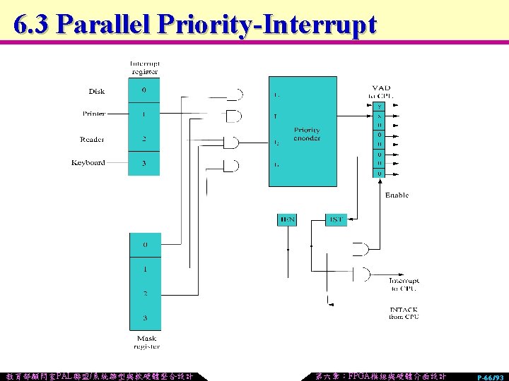
6. 3 Priority Interrupt u The system establishes a priority over the various sources to determine which condition is to be serviced first when two or more requests arrive simultaneously. u Two methods of priority interrupt. n Software priority-interrupt. l A polling procedure. n Hardware priority-interrupt. l Daisy-chaining priority. l Parallel priority-interrupt. 教育部顧問室PAL聯盟/系統雛型與軟硬體整合設計 第六章:FPGA模組與硬體介面設計 P-64/93
6. 3 Daisy-Chain Priority Interrupt Processor data bus 教育部顧問室PAL聯盟/系統雛型與軟硬體整合設計 第六章:FPGA模組與硬體介面設計 P-65/93
6. 3 DMA u Removing the CPU from the path and letting the I/O devices manage the memory directly. u During DMA transfer, the CPU is idle and has no control of the memory buses. u Two signals are used to facilitate the DMA transfer. n Bus request: a signal from DMA controller. n Bus grant: the CPU informs the DMA that the buses are in high-impedance state. Bus request BR CPU Bus grant BG 教育部顧問室PAL聯盟/系統雛型與軟硬體整合設計 DBUS Address bus ABUS Data bus RD Read WR Write High-impedance (disable) when BG is enable 第六章:FPGA模組與硬體介面設計 P-67/93
6. 3 DMA Controller u Block diagram of DMA controller. Address bus Data bus buffer DMA select DS Register select RS Read RD Write WR Bus request BR Bus grant BG Interrupt Control logic Interrupt 教育部顧問室PAL聯盟/系統雛型與軟硬體整合設計 Address buffer Address register Internal bus Data bus Word count register Control register DMA request DMA Acknowledge to I/O device 第六章:FPGA模組與硬體介面設計 P-68/93
6. 3 Initialization of DMA u The CPU initializes the DMA by sending the following information through the data bus. n Starting address of the memory block. n Word count. n Mode of transfer. n A start signal to do DMA transfer. 教育部顧問室PAL聯盟/系統雛型與軟硬體整合設計 第六章:FPGA模組與硬體介面設計 P-69/93
6. 3 DMA Transfer Interrupt Random-access memory (RAM) CPU BG BR RD WR Address Data Read control Write control Data bus Address select RD DS RS BR WR Address Direct memory access (DMA) controller BG Data DMA acknowledge DMA request I/O Peripheral device Interrupt 教育部顧問室PAL聯盟/系統雛型與軟硬體整合設計 第六章:FPGA模組與硬體介面設計 P-70/93
References u http: //www. xilinx. com/bvdocs/appnotes/xapp 611. pdf u http: //www. arm. com/products/solutions/AMBA_Spec. html u Mano, M. Morris, “Computer system architecture, ” Prentice Hall, 1993. 教育部顧問室PAL聯盟/系統雛型與軟硬體整合設計 第六章:FPGA模組與硬體介面設計 P-71/93