Chapter 11 Verilog HDL ApplicationSpecific Integrated Circuits Michael
- Slides: 48

Chapter 11 Verilog HDL Application-Specific Integrated Circuits Michael John Sebastian Smith Addison Wesley, 1997 EGRE 427 Advanced Digital Design

Verilog HDL l l l l Verilog is an alternative hardware description language to VHDL developed by Gateway Design Automation Cadence purchased Gateway and placed Verilog in the public domain (Open Verilog International - OVI) An IEEE standard version of Verilog was developed in 1995 [IEEE Std. 1364 -1995 Verilog LRM] In spite of this standardization, many flavors (usually vendor specific) of Verilog still persist Verilog syntax is much like C Verilog use is generally most prevalent on the West Coast (Silicon Valley) Most high-end commercial simulators support both VHDL and Verilog and you may receive IP blocks for your designs in Verilog which you will be expected to be able to work with OVI and VHDL International have recently merged further indicating a dual (or multi) language environment will become more prevalent EGRE 427 Advanced Digital Design

Verilog Identifiers l l l Identifiers (names of variables, wires, modules, etc. ) can contain any sequence of letters, numbers, ‘$’, or ‘_’ The first character of an identifier must be a letter or underscore Verilog identifiers are case sensitive reg legal_identifier, two__underscores; reg _OK, OK_$, CASE_SENSITIVE, case_sensitive; EGRE 427 Advanced Digital Design

Verilog Logic Values and Data Types l Verilog has a predefined logic-value system or value set: n l ‘ 0’, ‘ 1’, ‘x’, and ‘z’ Verilog has a limited number of data types: n n reg - like a variable, default value is ‘x’ and is updated immediately when on LHS of an assignment net - can not store values between assignments; default value is ‘z’; has subtypes: ¦ ¦ n n wire, tri supply 1, supply 0 integer time event real EGRE 427 Advanced Digital Design

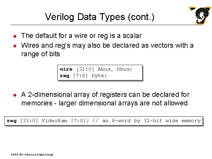
Verilog Data Types (cont. ) l l The default for a wire or reg is a scalar Wires and reg’s may also be declared as vectors with a range of bits wire [31: 0] Abus, Dbus; reg [7: 0] byte; l A 2 -dimensional array of registers can be declared for memories - larger dimensional arrays are not allowed reg [31: 0] Video. Ram [7: 0]; // an 8 -word by 32 -bit wide memory EGRE 427 Advanced Digital Design

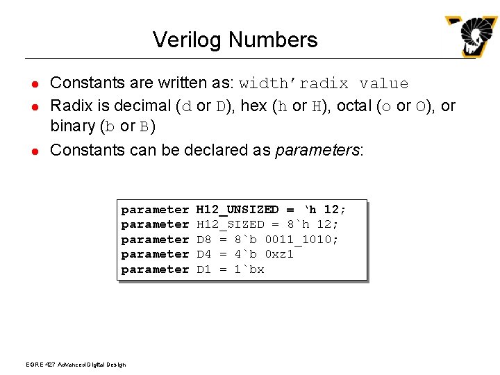
Verilog Numbers l l l Constants are written as: width’radix value Radix is decimal (d or D), hex (h or H), octal (o or O), or binary (b or B) Constants can be declared as parameters: parameter parameter EGRE 427 Advanced Digital Design H 12_UNSIZED = ‘h 12; H 12_SIZED = 8`h 12; D 8 = 8`b 0011_1010; D 4 = 4`b 0 xz 1 D 1 = 1`bx

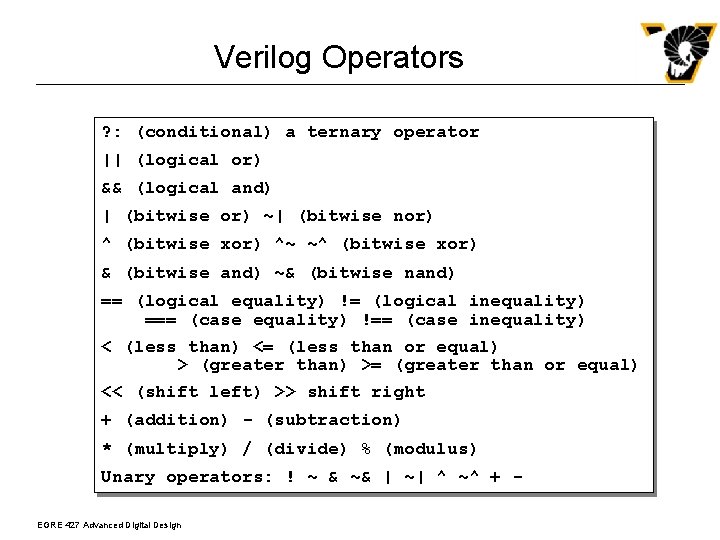
Verilog Operators ? : (conditional) a ternary operator || (logical or) && (logical and) | (bitwise or) ~| (bitwise nor) ^ (bitwise xor) ^~ ~^ (bitwise xor) & (bitwise and) ~& (bitwise nand) == (logical equality) != (logical inequality) === (case equality) !== (case inequality) < (less than) <= (less than or equal) > (greater than) >= (greater than or equal) << (shift left) >> shift right + (addition) - (subtraction) * (multiply) / (divide) % (modulus) Unary operators: ! ~ & ~& | ~| ^ ~^ + EGRE 427 Advanced Digital Design

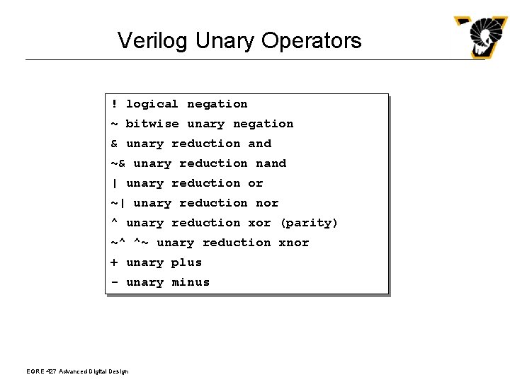
Verilog Unary Operators ! logical negation ~ bitwise unary negation & unary reduction and ~& unary reduction nand | unary reduction or ~| unary reduction nor ^ unary reduction xor (parity) ~^ ^~ unary reduction xnor + unary plus - unary minus EGRE 427 Advanced Digital Design

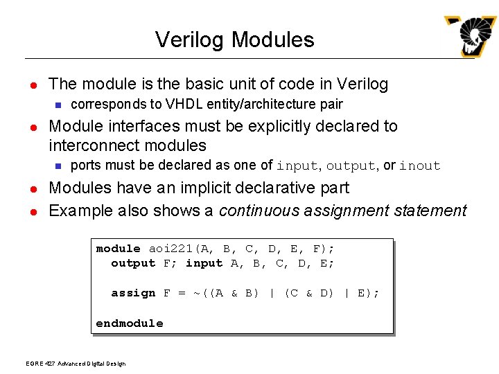
Verilog Modules l The module is the basic unit of code in Verilog n l Module interfaces must be explicitly declared to interconnect modules n l l corresponds to VHDL entity/architecture pair ports must be declared as one of input, output, or inout Modules have an implicit declarative part Example also shows a continuous assignment statement module aoi 221(A, B, C, D, E, F); output F; input A, B, C, D, E; assign F = ~((A & B) | (C & D) | E); endmodule EGRE 427 Advanced Digital Design

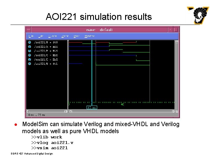
AOI 221 simulation results l Model. Sim can simulate Verilog and mixed-VHDL and Verilog models as well as pure VHDL models >>vlib work >>vlog aoi 221. v >>vsim aoi 221 EGRE 427 Advanced Digital Design

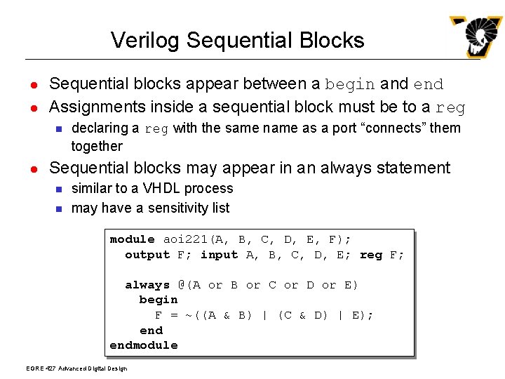
Verilog Sequential Blocks l l Sequential blocks appear between a begin and end Assignments inside a sequential block must be to a reg n l declaring a reg with the same name as a port “connects” them together Sequential blocks may appear in an always statement n n similar to a VHDL process may have a sensitivity list module aoi 221(A, B, C, D, E, F); output F; input A, B, C, D, E; reg F; always @(A or B or C or D or E) begin F = ~((A & B) | (C & D) | E); endmodule EGRE 427 Advanced Digital Design

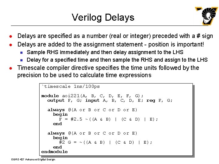
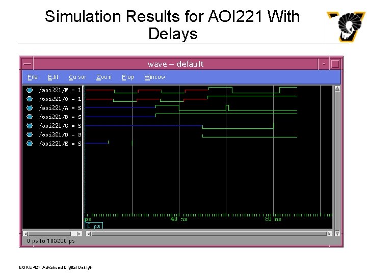
Verilog Delays l l Delays are specified as a number (real or integer) preceded with a # sign Delays are added to the assignment statement - position is important! n n l Sample RHS immediately and then delay assignment to the LHS Delay for a specified time and then sample the RHS and assign to the LHS Timescale compiler directive specifies the time units followed by the precision to be used to calculate time expressions `timescale 1 ns/100 ps module aoi 221(A, B, C, D, E, F, G); output F, G; input A, B, C, D, E; reg F, G; always @(A or B or C or D or E) begin F = #2. 5 ~((A & B) | (C & D) | E); end always @(A or B or C or D or E) begin #2 G = ~((A & B) | (C & D) | E); endmodule EGRE 427 Advanced Digital Design

Simulation Results for AOI 221 With Delays EGRE 427 Advanced Digital Design

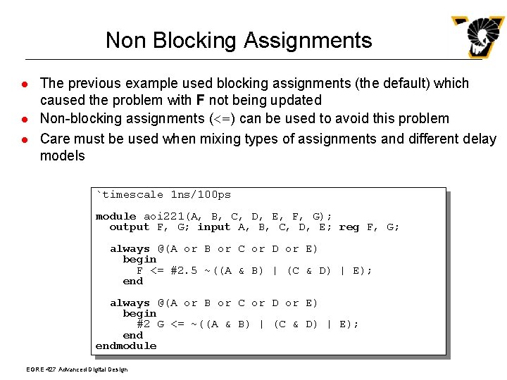
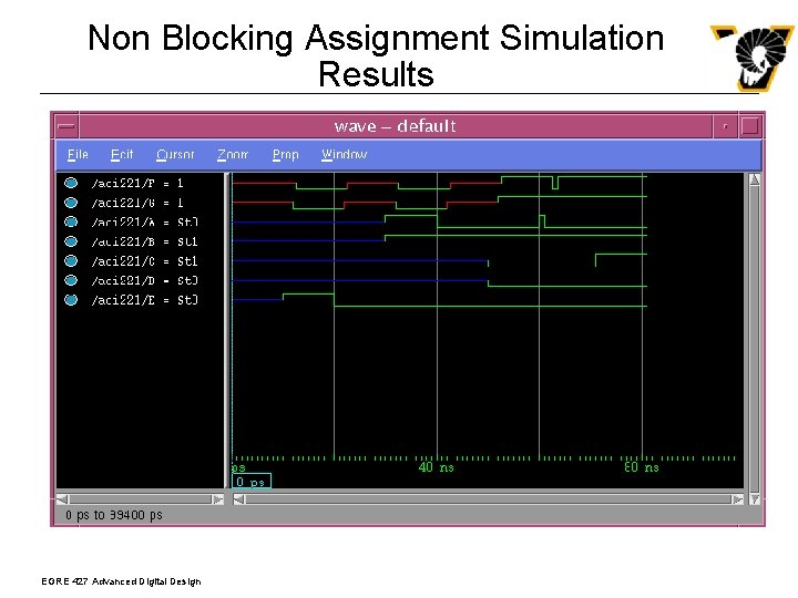
Non Blocking Assignments l l l The previous example used blocking assignments (the default) which caused the problem with F not being updated Non-blocking assignments (<=) can be used to avoid this problem Care must be used when mixing types of assignments and different delay models `timescale 1 ns/100 ps module aoi 221(A, B, C, D, E, F, G); output F, G; input A, B, C, D, E; reg F, G; always @(A or B or C or D or E) begin F <= #2. 5 ~((A & B) | (C & D) | E); end always @(A or B or C or D or E) begin #2 G <= ~((A & B) | (C & D) | E); endmodule EGRE 427 Advanced Digital Design

Non Blocking Assignment Simulation Results EGRE 427 Advanced Digital Design

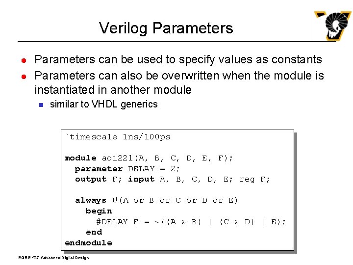
Verilog Parameters l l Parameters can be used to specify values as constants Parameters can also be overwritten when the module is instantiated in another module n similar to VHDL generics `timescale 1 ns/100 ps module aoi 221(A, B, C, D, E, F); parameter DELAY = 2; output F; input A, B, C, D, E; reg F; always @(A or B or C or D or E) begin #DELAY F = ~((A & B) | (C & D) | E); endmodule EGRE 427 Advanced Digital Design

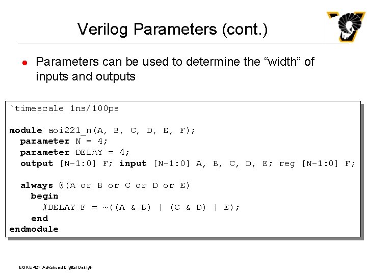
Verilog Parameters (cont. ) l Parameters can be used to determine the “width” of inputs and outputs `timescale 1 ns/100 ps module aoi 221_n(A, B, C, D, E, F); parameter N = 4; parameter DELAY = 4; output [N-1: 0] F; input [N-1: 0] A, B, C, D, E; reg [N-1: 0] F; always @(A or B or C or D or E) begin #DELAY F = ~((A & B) | (C & D) | E); endmodule EGRE 427 Advanced Digital Design

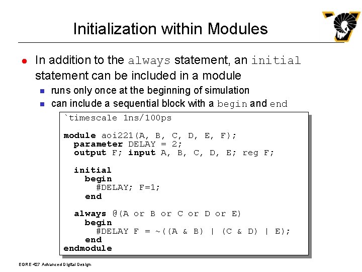
Initialization within Modules l In addition to the always statement, an initial statement can be included in a module n n runs only once at the beginning of simulation can include a sequential block with a begin and end `timescale 1 ns/100 ps module aoi 221(A, B, C, D, E, F); parameter DELAY = 2; output F; input A, B, C, D, E; reg F; initial begin #DELAY; F=1; end always @(A or B or C or D or E) begin #DELAY F = ~((A & B) | (C & D) | E); endmodule EGRE 427 Advanced Digital Design

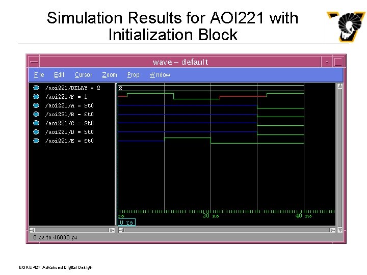
Simulation Results for AOI 221 with Initialization Block EGRE 427 Advanced Digital Design

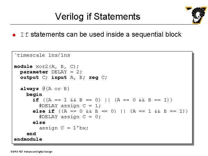
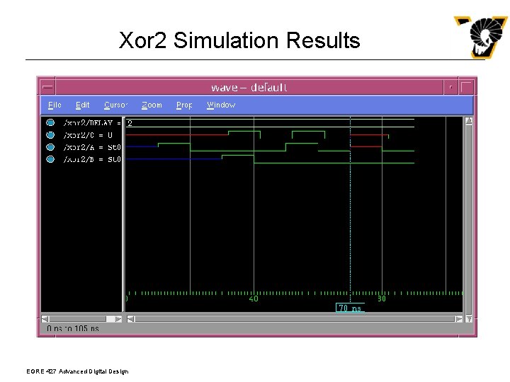
Verilog if Statements l If statements can be used inside a sequential block `timescale 1 ns/1 ns module xor 2(A, B, C); parameter DELAY = 2; output C; input A, B; reg C; always @(A or B) begin if ((A == 1 && B == #DELAY assign C = else if ((A == 0 && #DELAY assign C = else assign C = 1'bx; endmodule EGRE 427 Advanced Digital Design 0) || (A == 0 && B == 1)) 1; B == 0) || (A == 1 && B == 1)) 0;

Xor 2 Simulation Results EGRE 427 Advanced Digital Design

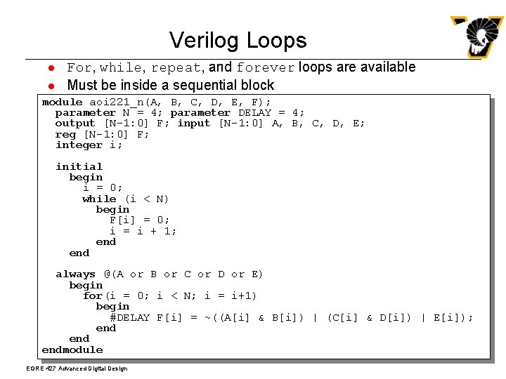
Verilog Loops l l For, while, repeat, and forever loops are available Must be inside a sequential block module aoi 221_n(A, B, C, D, E, F); parameter N = 4; parameter DELAY = 4; output [N-1: 0] F; input [N-1: 0] A, B, C, D, E; reg [N-1: 0] F; integer i; initial begin i = 0; while (i < N) begin F[i] = 0; i = i + 1; end always @(A or B or C or D or E) begin for(i = 0; i < N; i = i+1) begin #DELAY F[i] = ~((A[i] & B[i]) | (C[i] & D[i]) | E[i]); end endmodule EGRE 427 Advanced Digital Design

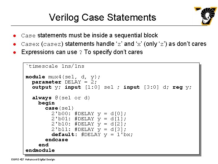
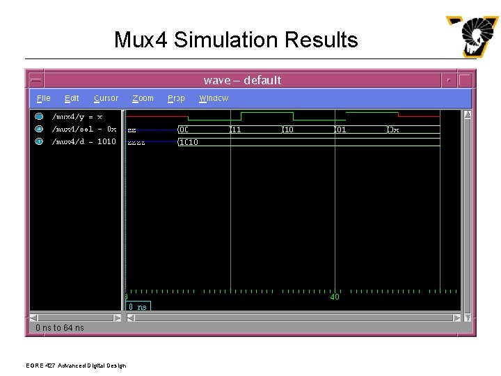
Verilog Case Statements l l l Case statements must be inside a sequential block Casex (casez) statements handle ‘z’ and ‘x’ (only ‘z’) as don’t cares Expressions can use ? To specify don’t cares `timescale 1 ns/1 ns module mux 4(sel, d, y); parameter DELAY = 2; output y; input [1: 0] sel ; input [3: 0] d; reg y; always @(sel or d) begin case(sel) 2'b 00: #DELAY y 2'b 01: #DELAY y 2'b 10: #DELAY y 2'b 11: #DELAY y default: #DELAY endcase endmodule EGRE 427 Advanced Digital Design = = y d[0]; d[1]; d[2]; d[3]; = 1'bx;

Mux 4 Simulation Results EGRE 427 Advanced Digital Design

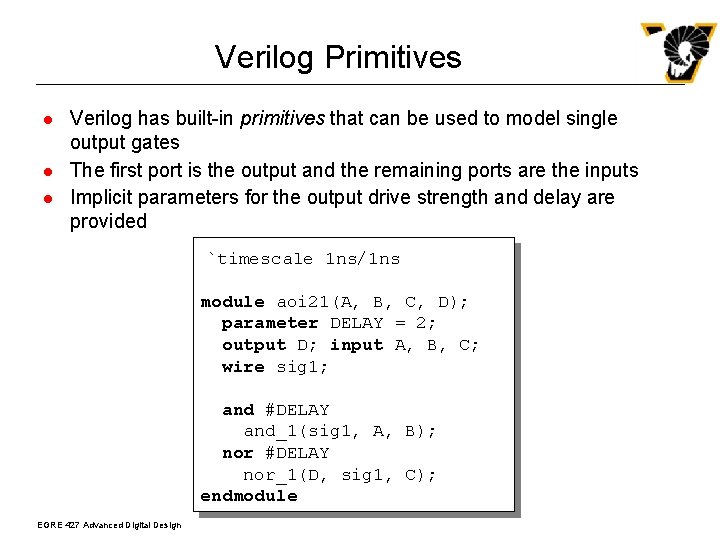
Verilog Primitives l l l Verilog has built-in primitives that can be used to model single output gates The first port is the output and the remaining ports are the inputs Implicit parameters for the output drive strength and delay are provided `timescale 1 ns/1 ns module aoi 21(A, B, C, D); parameter DELAY = 2; output D; input A, B, C; wire sig 1; and #DELAY and_1(sig 1, A, B); nor #DELAY nor_1(D, sig 1, C); endmodule EGRE 427 Advanced Digital Design

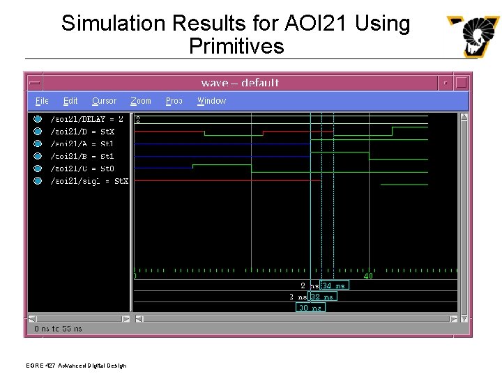
Simulation Results for AOI 21 Using Primitives EGRE 427 Advanced Digital Design

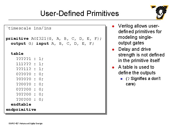
User-Defined Primitives `timescale 1 ns/1 ns l primitive AOI 321(G, A, B, C, D, E, F); output G; input A, B, C, D, E, F; table ? ? ? 1 : 111? ? ? : ? ? ? 11? : 0? ? 0? 0 : ? 0? 0? 0 : ? ? 00? 0 : 0? ? ? 00 : ? 0? ? 00 : ? ? 0? 00 : endtable endprimitive l 1; 1; 1; 0; 0; 0; EGRE 427 Advanced Digital Design l Verilog allows userdefined primitives for modeling singleoutput gates Delay and drive strength is not defined in the primitive itself A table is used to define the outputs n (? Signifies a don’t care)

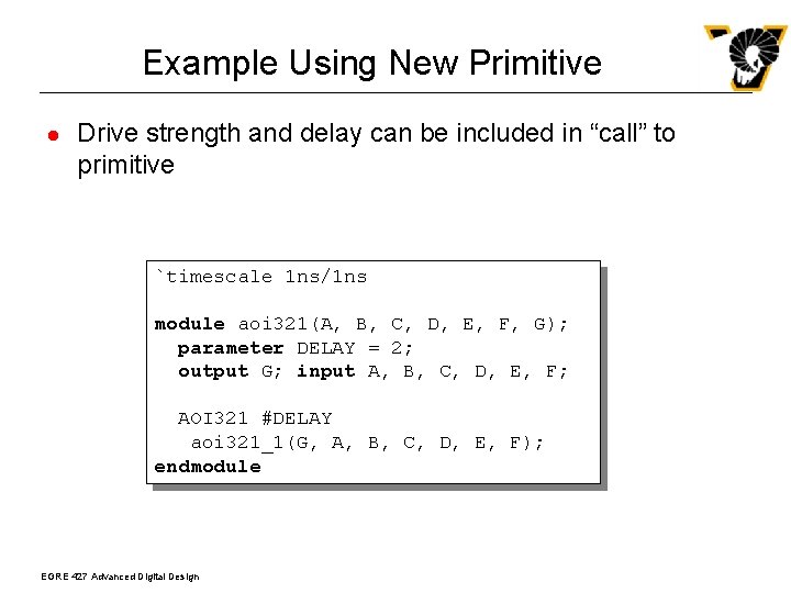
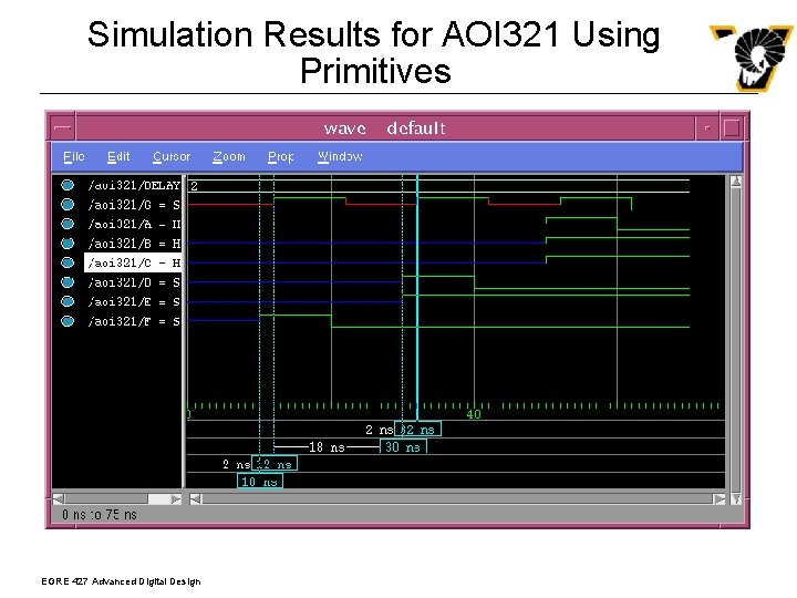
Example Using New Primitive l Drive strength and delay can be included in “call” to primitive `timescale 1 ns/1 ns module aoi 321(A, B, C, D, E, F, G); parameter DELAY = 2; output G; input A, B, C, D, E, F; AOI 321 #DELAY aoi 321_1(G, A, B, C, D, E, F); endmodule EGRE 427 Advanced Digital Design

Simulation Results for AOI 321 Using Primitives EGRE 427 Advanced Digital Design

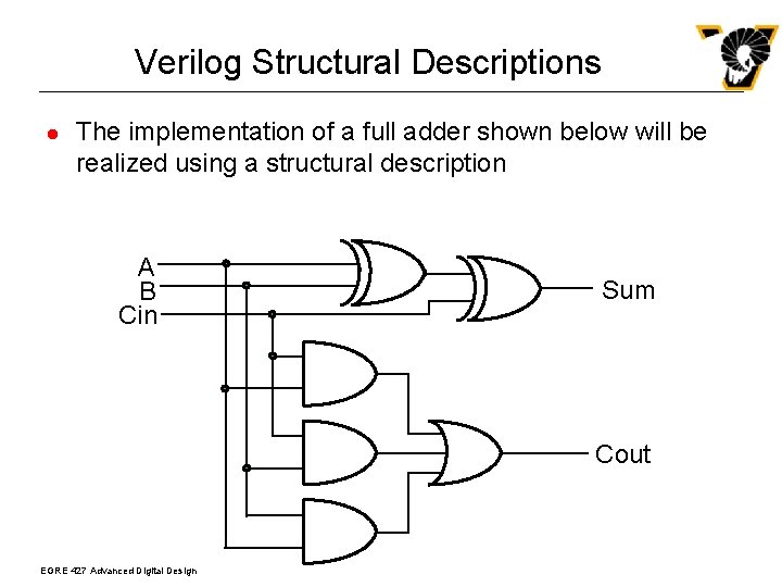
Verilog Structural Descriptions l The implementation of a full adder shown below will be realized using a structural description A B Cin Sum Cout EGRE 427 Advanced Digital Design

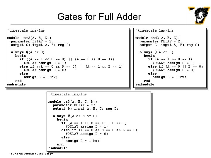
Gates for Full Adder `timescale 1 ns/1 ns module xor 2(A, B, C); parameter DELAY = 2; output C; input A, B; reg C; module and 2(A, B, C); parameter DELAY = 2; output C; input A, B; reg C; always @(A or B) begin if ((A == 1 && B == #DELAY assign C = else if ((A == 0 && #DELAY assign C = else assign C = 1'bx; endmodule always @(A or B) begin if (A == 1 && B == 1) #DELAY assign C = 1; else if (A == 0 || B == 0) #DELAY assign C = 0; else assign C = 1'bx; endmodule 0) || (A == 0 && B == 1)) 1; B == 0) || (A == 1 && B == 1)) 0; `timescale 1 ns/1 ns module or 3(A, B, C, D); parameter DELAY = 2; output D; input A, B, C; reg D; always @(A or B or C) begin if (A == 1 || B == 1 || C == 1) #DELAY assign D = 1; else if (A == 0 && B == 0 && C == 0) #DELAY assign D = 0; else assign D = 1'bx; endmodule EGRE 427 Advanced Digital Design

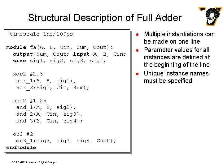
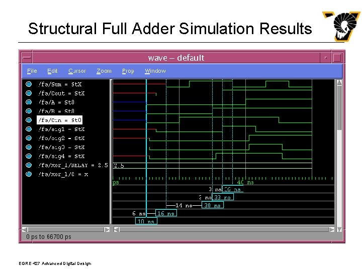
Structural Description of Full Adder `timescale 1 ns/100 ps module fa(A, B, Cin, Sum, Cout); output Sum, Cout; input A, B, Cin; wire sig 1, sig 2, sig 3, sig 4; xor 2 #2. 5 xor_1(A, B, sig 1), xor_2(sig 1, Cin, Sum); and 2 #1. 25 and_1(A, B, sig 2), and_2(A, Cin, sig 3), and_3(B, Cin, sig 4); or 3 #2 or 3_1(sig 2, sig 3, sig 4, Cout); endmodule EGRE 427 Advanced Digital Design l l l Multiple instantiations can be made on one line Parameter values for all instances are defined at the beginning of the line Unique instance names must be specified

Structural Full Adder Simulation Results EGRE 427 Advanced Digital Design

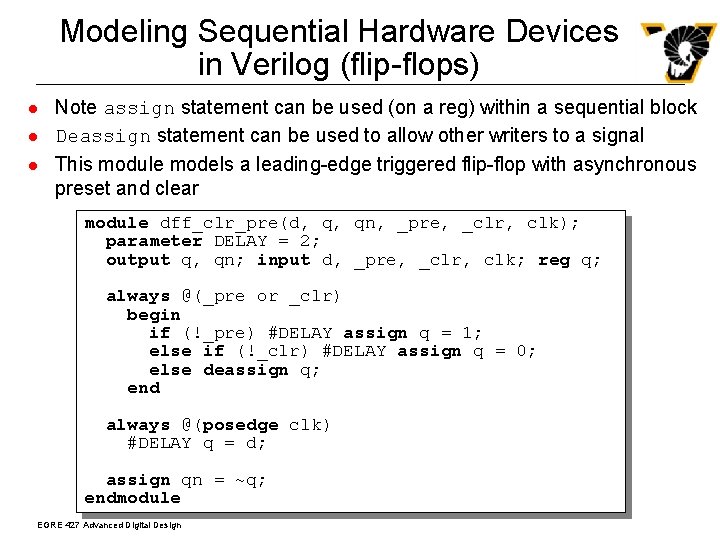
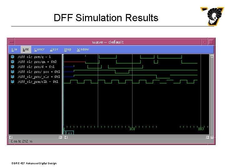
Modeling Sequential Hardware Devices in Verilog (flip-flops) l l l Note assign statement can be used (on a reg) within a sequential block Deassign statement can be used to allow other writers to a signal This module models a leading-edge triggered flip-flop with asynchronous preset and clear module dff_clr_pre(d, q, qn, _pre, _clr, clk); parameter DELAY = 2; output q, qn; input d, _pre, _clr, clk; reg q; always @(_pre or _clr) begin if (!_pre) #DELAY assign q = 1; else if (!_clr) #DELAY assign q = 0; else deassign q; end always @(posedge clk) #DELAY q = d; assign qn = ~q; endmodule EGRE 427 Advanced Digital Design

DFF Simulation Results EGRE 427 Advanced Digital Design

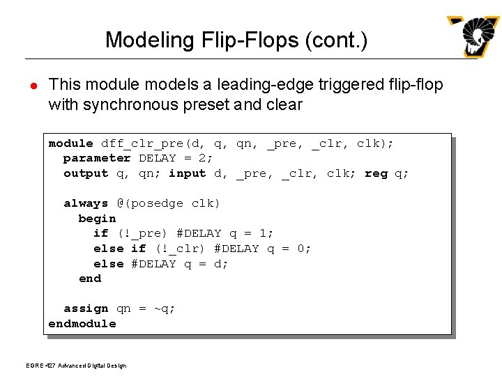
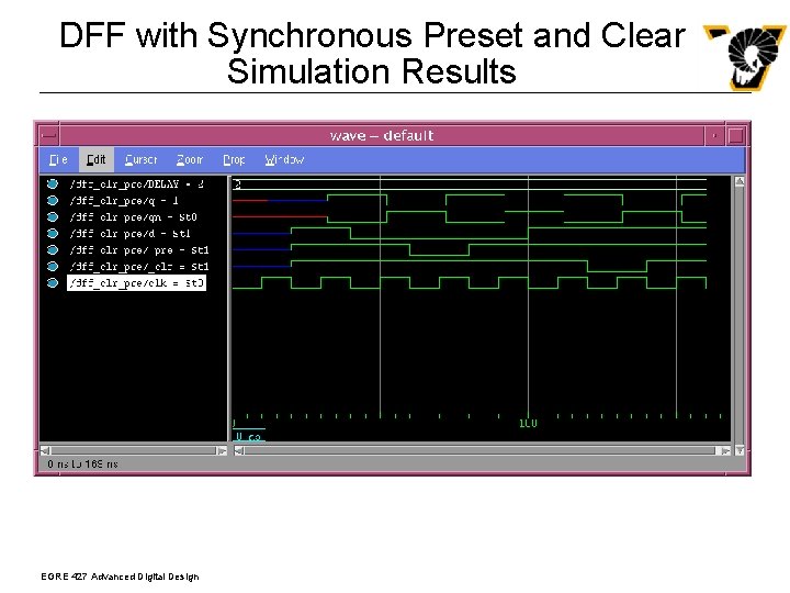
Modeling Flip-Flops (cont. ) l This module models a leading-edge triggered flip-flop with synchronous preset and clear module dff_clr_pre(d, q, qn, _pre, _clr, clk); parameter DELAY = 2; output q, qn; input d, _pre, _clr, clk; reg q; always @(posedge clk) begin if (!_pre) #DELAY q = 1; else if (!_clr) #DELAY q = 0; else #DELAY q = d; end assign qn = ~q; endmodule EGRE 427 Advanced Digital Design

DFF with Synchronous Preset and Clear Simulation Results EGRE 427 Advanced Digital Design

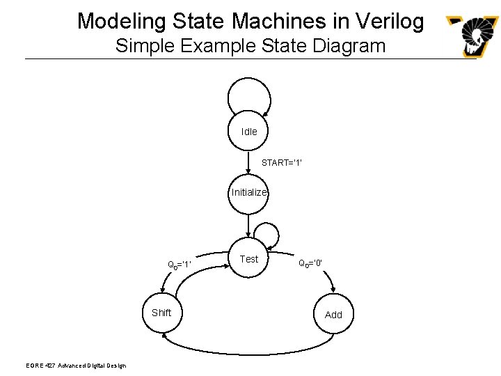
Modeling State Machines in Verilog Simple Example State Diagram Idle START=‘ 1’ Initialize Q 0=‘ 1’ Shift EGRE 427 Advanced Digital Design Test Q 0=‘ 0’ Add

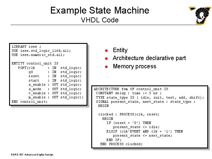
Example State Machine VHDL Code LIBRARY ieee ; USE ieee. std_logic_1164. all; USE ieee. numeric_std. all; ENTITY control_unit IS PORT(clk : IN q 0 : IN reset : IN start : IN a_enable : OUT a_mode : OUT c_enable : OUT m_enable : OUT END control_unit; std_logic; std_logic; std_logic); l l l Entity Architecture declarative part Memory process ARCHITECTURE fsm OF control_unit IS CONSTANT delay : time : = 5 ns ; TYPE state_type IS ( idle, init, test, add, shift); SIGNAL present_state, next_state : state_type ; BEGIN clocked : PROCESS(clk, reset) BEGIN IF (reset = '0') THEN present_state <= idle; ELSIF (clk'EVENT AND clk = '1') THEN present_state <= next_state; END IF; END PROCESS clocked; EGRE 427 Advanced Digital Design

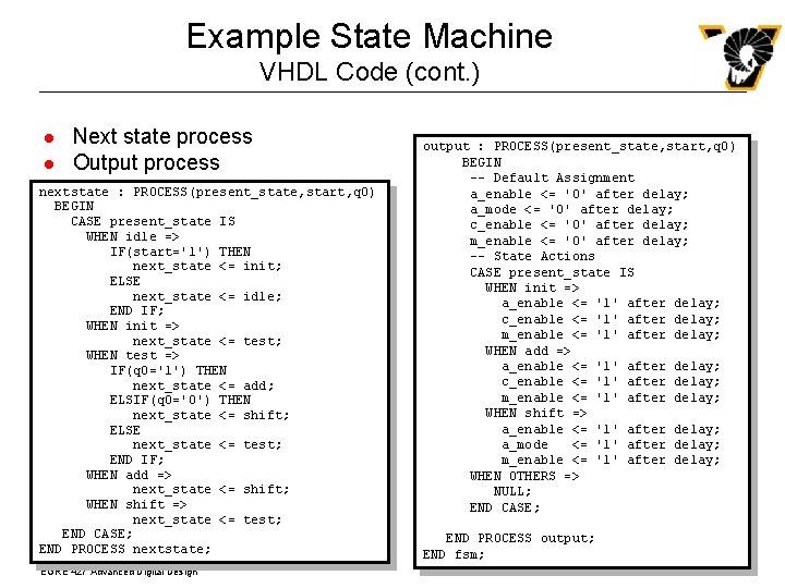
Example State Machine VHDL Code (cont. ) l l Next state process Output process nextstate : PROCESS(present_state, start, q 0) BEGIN CASE present_state IS WHEN idle => IF(start='1') THEN next_state <= init; ELSE next_state <= idle; END IF; WHEN init => next_state <= test; WHEN test => IF(q 0='1') THEN next_state <= add; ELSIF(q 0='0') THEN next_state <= shift; ELSE next_state <= test; END IF; WHEN add => next_state <= shift; WHEN shift => next_state <= test; END CASE; END PROCESS nextstate; EGRE 427 Advanced Digital Design output : PROCESS(present_state, start, q 0) BEGIN -- Default Assignment a_enable <= '0' after delay; a_mode <= '0' after delay; c_enable <= '0' after delay; m_enable <= '0' after delay; -- State Actions CASE present_state IS WHEN init => a_enable <= '1' after delay; c_enable <= '1' after delay; m_enable <= '1' after delay; WHEN add => a_enable <= '1' after delay; c_enable <= '1' after delay; m_enable <= '1' after delay; WHEN shift => a_enable <= '1' after delay; a_mode <= '1' after delay; m_enable <= '1' after delay; WHEN OTHERS => NULL; END CASE; END PROCESS output; END fsm;

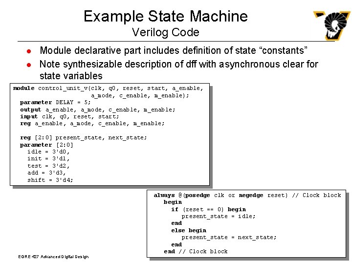
Example State Machine Verilog Code l l Module declarative part includes definition of state “constants” Note synthesizable description of dff with asynchronous clear for state variables module control_unit_v(clk, q 0, reset, start, a_enable, a_mode, c_enable, m_enable); parameter DELAY = 5; output a_enable, a_mode, c_enable, m_enable; input clk, q 0, reset, start; reg a_enable, a_mode, c_enable, m_enable; reg [2: 0] present_state, next_state; parameter [2: 0] idle = 3'd 0, init = 3'd 1, test = 3'd 2, add = 3'd 3, shift = 3'd 4; EGRE 427 Advanced Digital Design always @(posedge clk or negedge reset) // Clock begin if (reset == 0) begin present_state = idle; end else begin present_state = next_state; end // Clock block

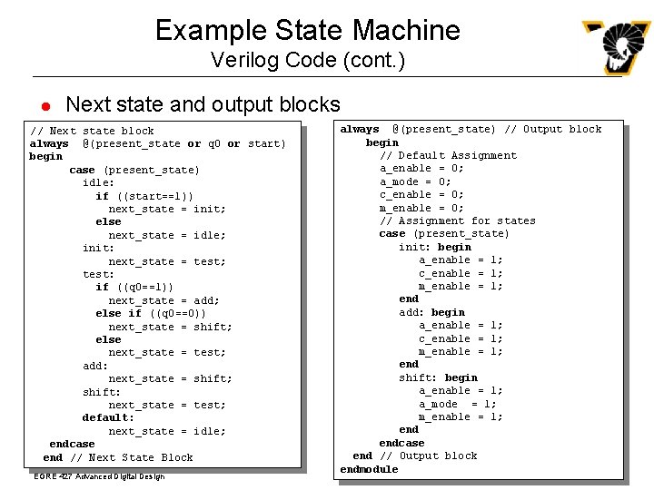
Example State Machine Verilog Code (cont. ) l Next state and output blocks // Next state block always @(present_state or q 0 or start) begin case (present_state) idle: if ((start==1)) next_state = init; else next_state = idle; init: next_state = test; test: if ((q 0==1)) next_state = add; else if ((q 0==0)) next_state = shift; else next_state = test; add: next_state = shift; shift: next_state = test; default: next_state = idle; endcase end // Next State Block EGRE 427 Advanced Digital Design always @(present_state) // Output block begin // Default Assignment a_enable = 0; a_mode = 0; c_enable = 0; m_enable = 0; // Assignment for states case (present_state) init: begin a_enable = 1; c_enable = 1; m_enable = 1; end add: begin a_enable = 1; c_enable = 1; m_enable = 1; end shift: begin a_enable = 1; a_mode = 1; m_enable = 1; endcase end // Output block endmodule

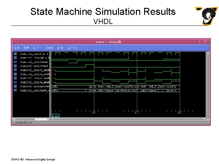
State Machine Simulation Results VHDL EGRE 427 Advanced Digital Design

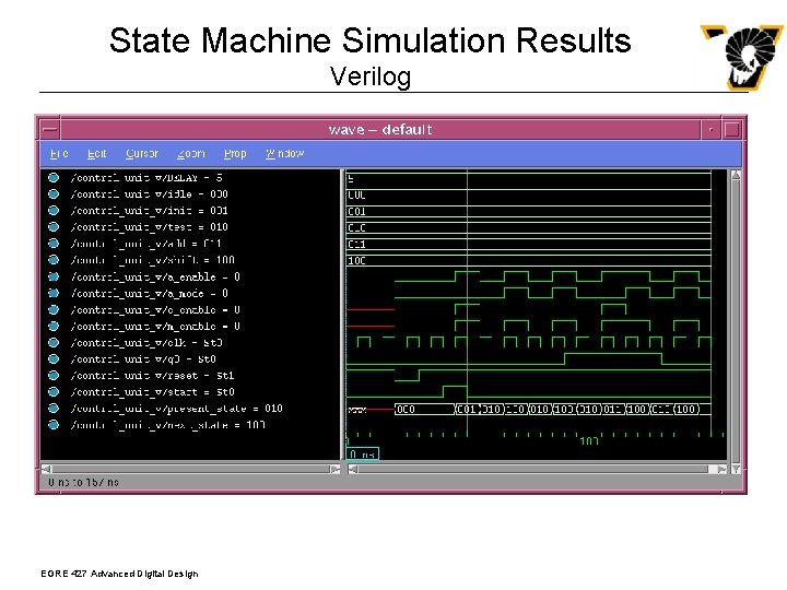
State Machine Simulation Results Verilog EGRE 427 Advanced Digital Design

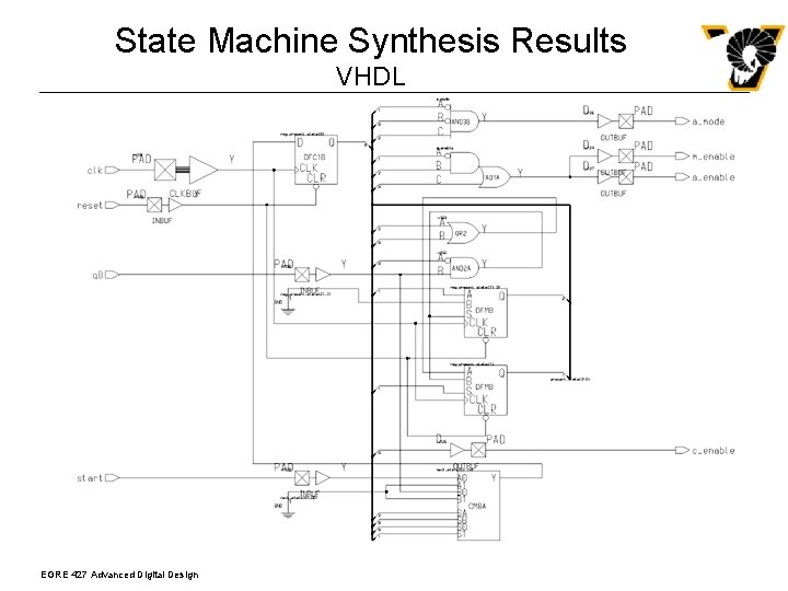
State Machine Synthesis Results VHDL EGRE 427 Advanced Digital Design

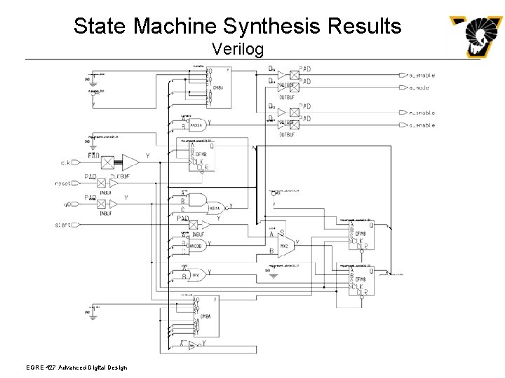
State Machine Synthesis Results Verilog EGRE 427 Advanced Digital Design

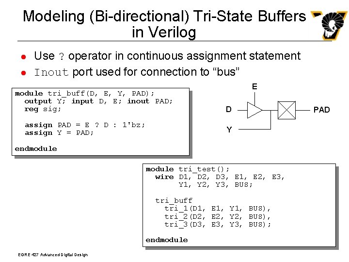
Modeling (Bi-directional) Tri-State Buffers in Verilog l l Use ? operator in continuous assignment statement Inout port used for connection to “bus” module tri_buff(D, E, Y, PAD); output Y; input D, E; inout PAD; reg sig; assign PAD = E ? D : 1'bz; assign Y = PAD; E D Y endmodule tri_test(); wire D 1, D 2, D 3, E 1, E 2, E 3, Y 1, Y 2, Y 3, BUS; tri_buff tri_1(D 1, E 1, Y 1, BUS), tri_2(D 2, E 2, Y 2, BUS), tri_3(D 3, E 3, Y 3, BUS); endmodule EGRE 427 Advanced Digital Design PAD

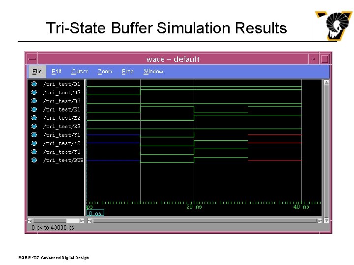
Tri-State Buffer Simulation Results EGRE 427 Advanced Digital Design