Introduction to Microcontrollers ApplicationSpecific Integrated Circuits Michael John
- Slides: 123

Introduction to Microcontrollers Application-Specific Integrated Circuits Michael John Sebastian Smith Addison Wesley, 1997 EGRE 427 Advanced Digital Design

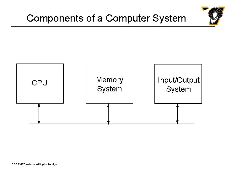
Components of a Computer System CPU EGRE 427 Advanced Digital Design Memory System Input/Output System

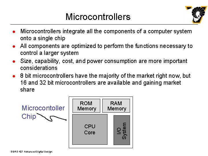
Microcontrollers l l l Microcontrollers integrate all the components of a computer system onto a single chip All components are optimized to perform the functions necessary to control a larger system Size, capability, cost, and power consumption are more important considerations 8 bit microcontrollers have the majority of the market right now, but 16 and 32 bit microcontrollers are available and gaining market share Microcontoller Chip EGRE 427 Advanced Digital Design ROM Memory RAM Memory CPU Core I/O System l

Microcontroller Components l CPU n n l May be an adaptation of an existing microprocessor or a completely new architecture Instruction set is typically modified to deal with new I/O system Memory n n n On-chip NVRM to hold program - can be mask programmable ROM, OTP ROM, or EPROM/EEPROM On-chip RAM for variable storage - usually small amount and can double as m. P’s registers Both can be expanded using off-chip memory (extended microcontroller mode) EGRE 427 Advanced Digital Design

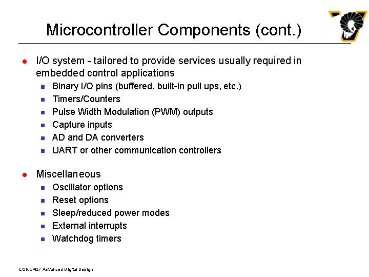
Microcontroller Components (cont. ) l I/O system - tailored to provide services usually required in embedded control applications n n n l Binary I/O pins (buffered, built-in pull ups, etc. ) Timers/Counters Pulse Width Modulation (PWM) outputs Capture inputs AD and DA converters UART or other communication controllers Miscellaneous n n n Oscillator options Reset options Sleep/reduced power modes External interrupts Watchdog timers EGRE 427 Advanced Digital Design

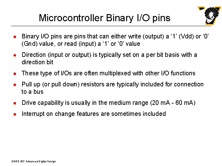
Microcontroller Binary I/O pins l Binary I/O pins are pins that can either write (output) a ‘ 1’ (Vdd) or ‘ 0’ (Gnd) value, or read (input) a ‘ 1’ or ‘ 0’ value l Direction (input or output) is typically set on a per bit basis with a direction bit l These type of I/Os are often multiplexed with other I/O functions l Pull up (or pull down) resistors are typically included for connection to a bus l Drive capability is usually in the medium range (20 m. A - 60 m. A) l Interrupt on change features are sometimes included EGRE 427 Advanced Digital Design

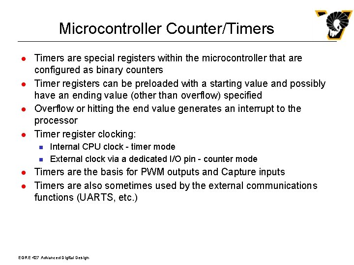
Microcontroller Counter/Timers l l Timers are special registers within the microcontroller that are configured as binary counters Timer registers can be preloaded with a starting value and possibly have an ending value (other than overflow) specified Overflow or hitting the end value generates an interrupt to the processor Timer register clocking: n n l l Internal CPU clock - timer mode External clock via a dedicated I/O pin - counter mode Timers are the basis for PWM outputs and Capture inputs Timers are also sometimes used by the external communications functions (UARTS, etc. ) EGRE 427 Advanced Digital Design

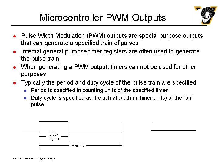
Microcontroller PWM Outputs l l Pulse Width Modulation (PWM) outputs are special purpose outputs that can generate a specified train of pulses Internal general purpose timer registers are often used to generate the pulse train When generating a PWM output, timers can not be used for other purposes Typically the period and duty cycle of the pulse train are specified n n Period is specified in counting units of the specified timer Duty cycle is specified as the actual width (in timer units) of the “on” pulse Duty Cycle Period EGRE 427 Advanced Digital Design

Microcontroller Capture Inputs l Capture inputs are used to count external events l A general purpose timer is associated with each capture register l The timer is incremented each time the external event occurs l The external event can be a rising or falling edge on the capture input, or multiples there of (i. e. , every 4 th rising/falling edge, every 16 th rising/falling edge) l The capture (timer) register value can be read or an interrupt can be generated when it equals a specified value EGRE 427 Advanced Digital Design

Other Microcontroller I/O functions l Some microcontrollers include an internal Analog-to-Digital converter (some with multiple channels) l Conversion values are placed in a special purpose register l Conversion is started under software control l Accuracy (no. of bits) is variable, but is typically in the 8 -16 bit range l Input voltage usually in the range of 0 to 2 X or 3 X Vdd l Digital-to-Analog converters are also sometimes provided l Input is typically one or two processor data words wide l Output is 0 to 2 X or 3 X Vdd l Current drive is equivalent to other I/O ports EGRE 427 Advanced Digital Design

Other Microcontroller I/O functions (etc. ) l l Most microcontrollers include built-in serial communications capabilities n Universal Asynchronous Receiver/Transmitter (UART) n Serial Peripheral Interface (SPIâ) n Microwireâ n I 2 C Most microcontrollers also include the following capabilities for dealing with real-time systems: n Optional oscillator sources such as external clock, external crystal, or simple RC timing circuit n Watchdog timers that will interrupt the CPU after a certain period of time if the CPU does not reset it - useful for recovering from software malfunctions n Power-down or sleep modes from which wake-up occurs on interrupts (from watchdog timer, timer/counters, capture inputs, external interrupts, etc. ) EGRE 427 Advanced Digital Design

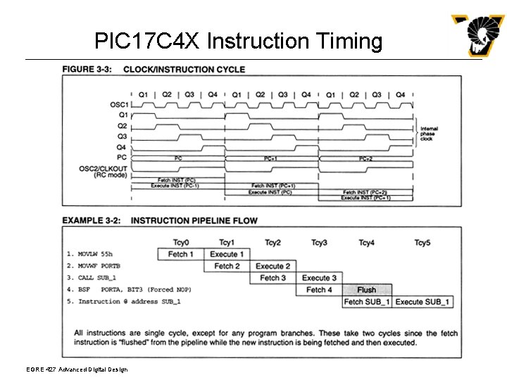
Microchip PIC 17 C 4 X Series Microcontrollers l Harvard architecture - 16 bit instructions, 8 bit data l RISC instruction set - 58 total instructions l Single cycle (4 clock cycles) instruction execution except for program branches and table operation which require 2 cycles l DC (0 Hz) to 33 MHz clock input - DC to 121 ns instruction cycle time l Hardware multiplier (except PIC 17 C 42 l 40 pin DIP package l EPROM 2 K, 4 K, and 8 K X 16 options n n l External program memory up to 64 K X 16 can be used (requires the elimination of 16 I/O pins) UV EPROM OTP Manufacturer Programmed Data RAM 232 or 454 bytes available EGRE 427 Advanced Digital Design

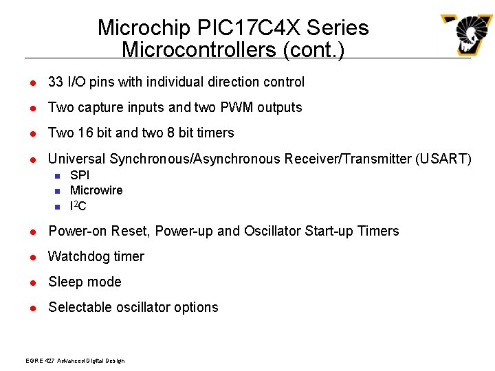
Microchip PIC 17 C 4 X Series Microcontrollers (cont. ) l 33 I/O pins with individual direction control l Two capture inputs and two PWM outputs l Two 16 bit and two 8 bit timers l Universal Synchronous/Asynchronous Receiver/Transmitter (USART) n n n SPI Microwire I 2 C l Power-on Reset, Power-up and Oscillator Start-up Timers l Watchdog timer l Sleep mode l Selectable oscillator options EGRE 427 Advanced Digital Design

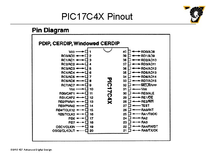
PIC 17 C 4 X Pinout EGRE 427 Advanced Digital Design

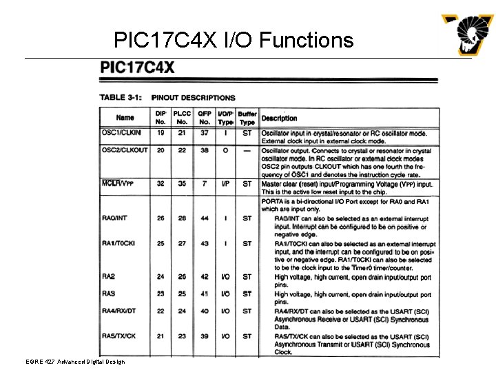
PIC 17 C 4 X I/O Functions EGRE 427 Advanced Digital Design

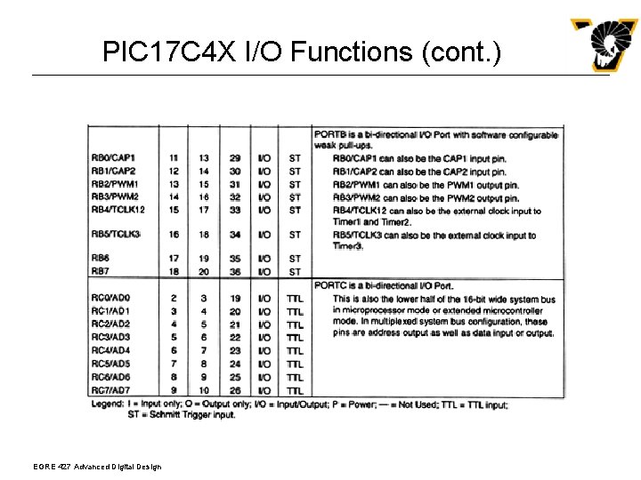
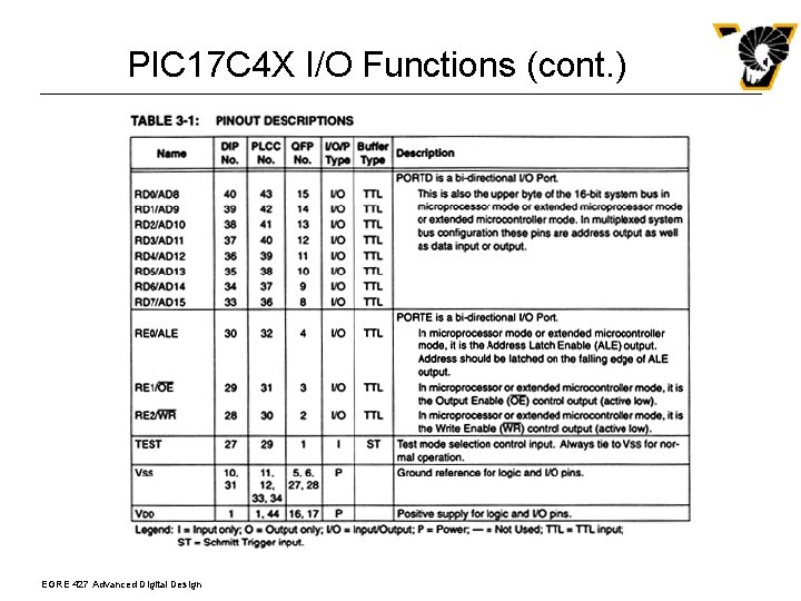
PIC 17 C 4 X I/O Functions (cont. ) EGRE 427 Advanced Digital Design

PIC 17 C 4 X I/O Functions (cont. ) EGRE 427 Advanced Digital Design

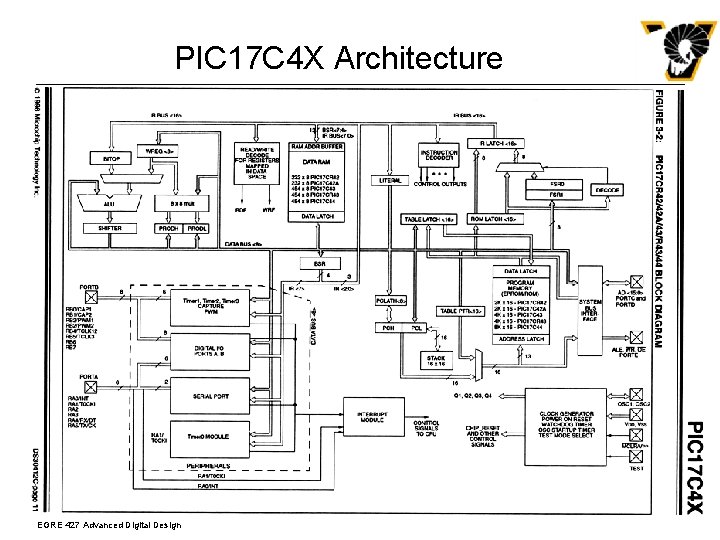
PIC 17 C 4 X Architecture EGRE 427 Advanced Digital Design

PIC 17 C 4 X Instruction Timing EGRE 427 Advanced Digital Design

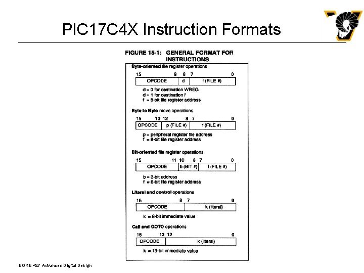
PIC 17 C 4 X Instruction Formats EGRE 427 Advanced Digital Design

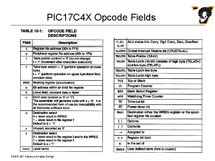
PIC 17 C 4 X Opcode Fields EGRE 427 Advanced Digital Design

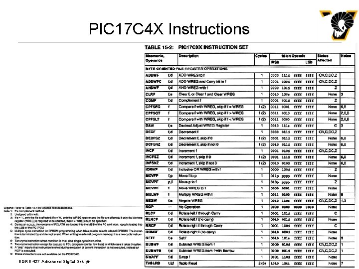
PIC 17 C 4 X Instructions EGRE 427 Advanced Digital Design

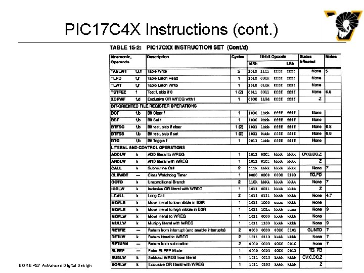
PIC 17 C 4 X Instructions (cont. ) EGRE 427 Advanced Digital Design

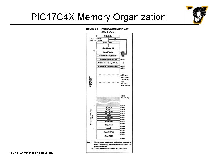
PIC 17 C 4 X Memory Organization EGRE 427 Advanced Digital Design

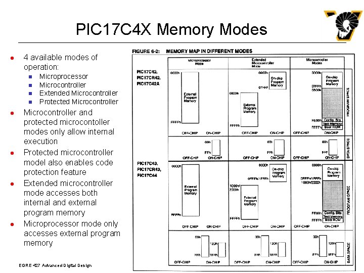
PIC 17 C 4 X Memory Modes l 4 available modes of operation: n n l l Microprocessor Microcontroller Extended Microcontroller Protected Microcontroller and protected microcontoller modes only allow internal execution Protected microcontroller model also enables code protection feature Extended microcontroller mode accesses both internal and external program memory Microprocessor mode only accesses external program memory EGRE 427 Advanced Digital Design

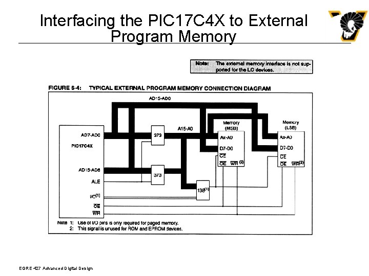
Interfacing the PIC 17 C 4 X to External Program Memory EGRE 427 Advanced Digital Design

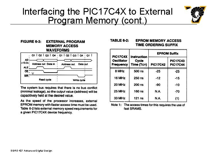
Interfacing the PIC 17 C 4 X to External Program Memory (cont. ) EGRE 427 Advanced Digital Design

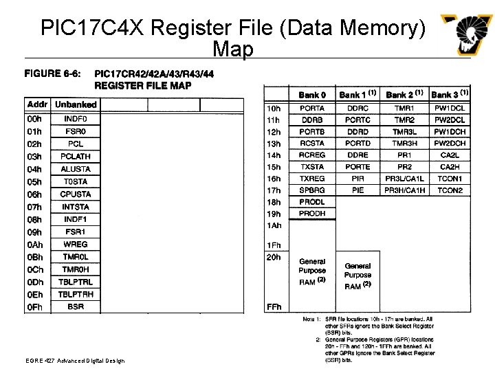
PIC 17 C 4 X Register File (Data Memory) Map EGRE 427 Advanced Digital Design

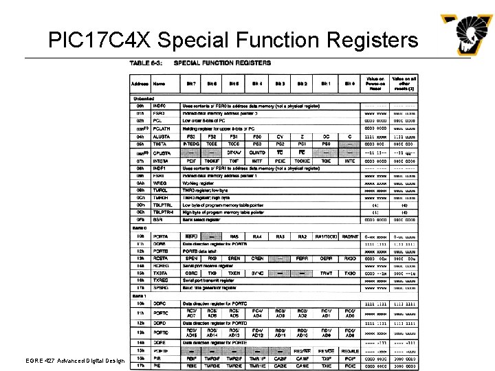
PIC 17 C 4 X Special Function Registers EGRE 427 Advanced Digital Design

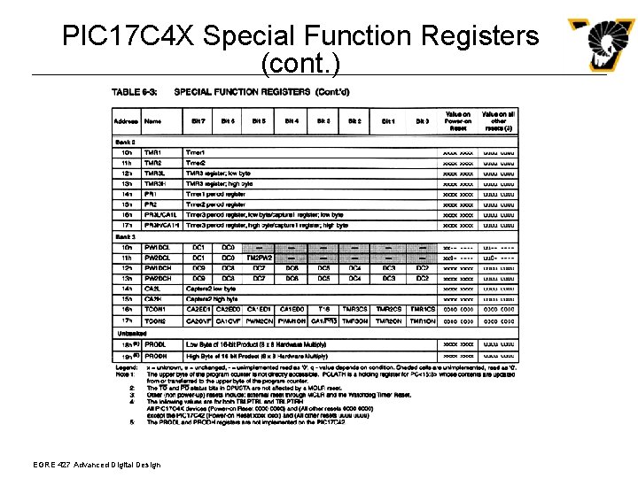
PIC 17 C 4 X Special Function Registers (cont. ) EGRE 427 Advanced Digital Design

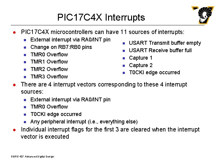
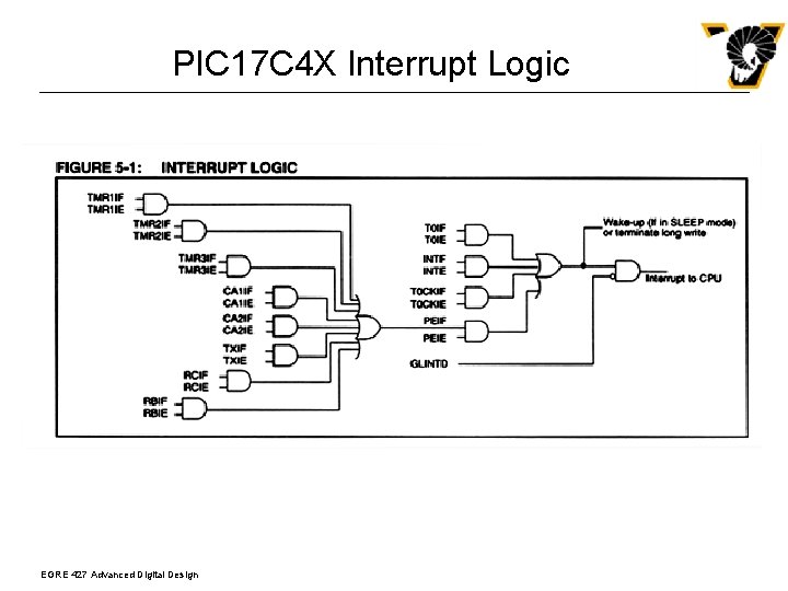
PIC 17 C 4 X Interrupts l PIC 17 C 4 X microcontrollers can have 11 sources of interrupts: n n n l n n n USART Transmit buffer empty USART Receive buffer full Capture 1 Capture 2 T 0 CKI edge occurred There are 4 interrupt vectors corresponding to these 4 interrupt sources: n n l External interrupt via RA 0/INT pin Change on RB 7: RB 0 pins TMR 0 Overflow TMR 1 Overflow TMR 2 Overflow TMR 3 Overflow External interrupt via RA 0/INT pin TMR 0 Overflow T 0 CKI edge occurred Any peripheral interrupt (i. e. , everything else) Individual interrupt flags for the first 3 are cleared when the interrupt vector is executed EGRE 427 Advanced Digital Design

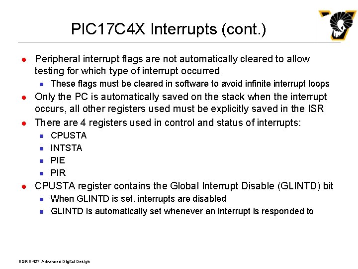
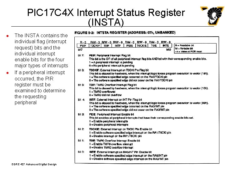
PIC 17 C 4 X Interrupts (cont. ) l Peripheral interrupt flags are not automatically cleared to allow testing for which type of interrupt occurred n l l Only the PC is automatically saved on the stack when the interrupt occurs, all other registers used must be explicitly saved in the ISR There are 4 registers used in control and status of interrupts: n n l These flags must be cleared in software to avoid infinite interrupt loops CPUSTA INTSTA PIE PIR CPUSTA register contains the Global Interrupt Disable (GLINTD) bit n n When GLINTD is set, interrupts are disabled GLINTD is automatically set whenever an interrupt is responded to EGRE 427 Advanced Digital Design

PIC 17 C 4 X Interrupt Logic EGRE 427 Advanced Digital Design

PIC 17 C 4 X Interrupt Status Register (INSTA) l l The INSTA contains the individual flag (interrupt request) bits and the individual interrupt enable bits for the four major types of interrupts If a peripheral interrupt occurred, the PIR register must be examined to determine the requesting peripheral EGRE 427 Advanced Digital Design

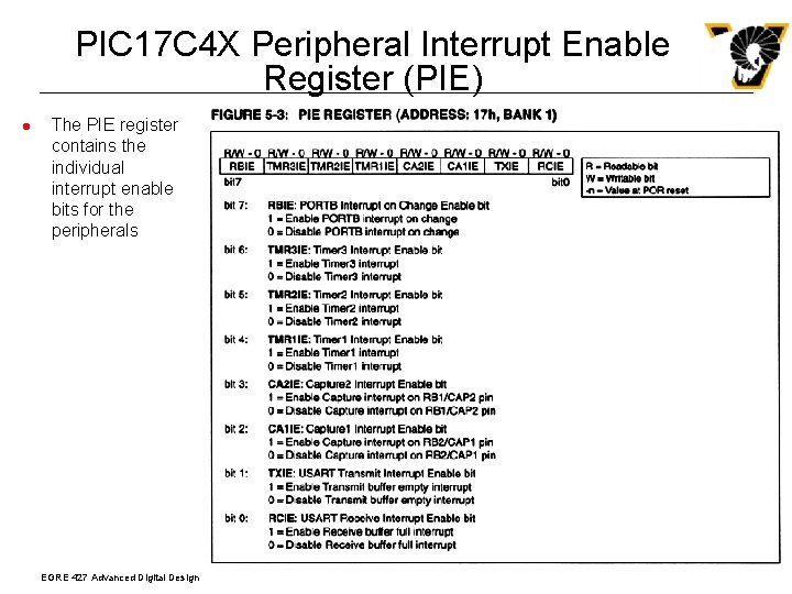
PIC 17 C 4 X Peripheral Interrupt Enable Register (PIE) l The PIE register contains the individual interrupt enable bits for the peripherals EGRE 427 Advanced Digital Design

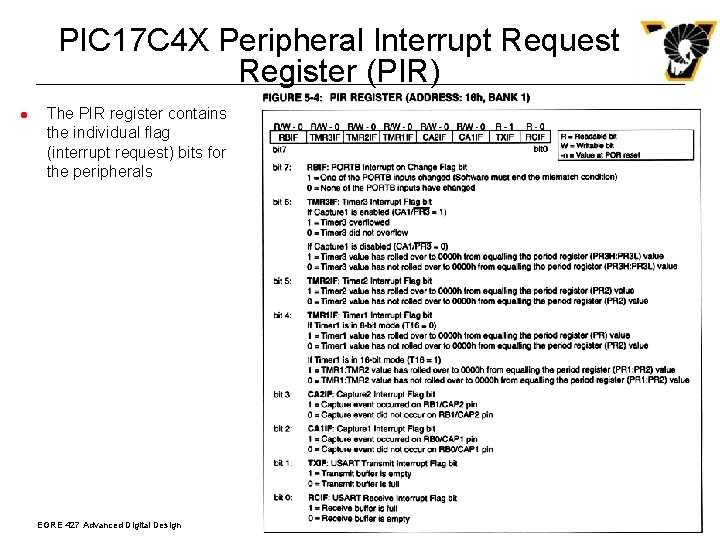
PIC 17 C 4 X Peripheral Interrupt Request Register (PIR) l The PIR register contains the individual flag (interrupt request) bits for the peripherals EGRE 427 Advanced Digital Design

PIC 17 C 4 X I/O Ports l l PIC 17 C 4 X micrcontollers have five I/O ports - PORTA through PORTE PORTB through PORTE have a corresponding Data Direction Register (DDRX) to configure pins as either inputs or outputs PORTC, PORTD, and PORTE pins are multiplexed with the system bus - these ports are not available in the microprocessor or extended microcontroller modes PORTA and PORTB are multiplexed with the peripheral features of the microcontroller n n n Timer modules Capture module PWM module USART module External interrupt pins The PWM and USART modules automatically configure their I/O pins - the other modules must have their DDR bits configured appropriately EGRE 427 Advanced Digital Design l

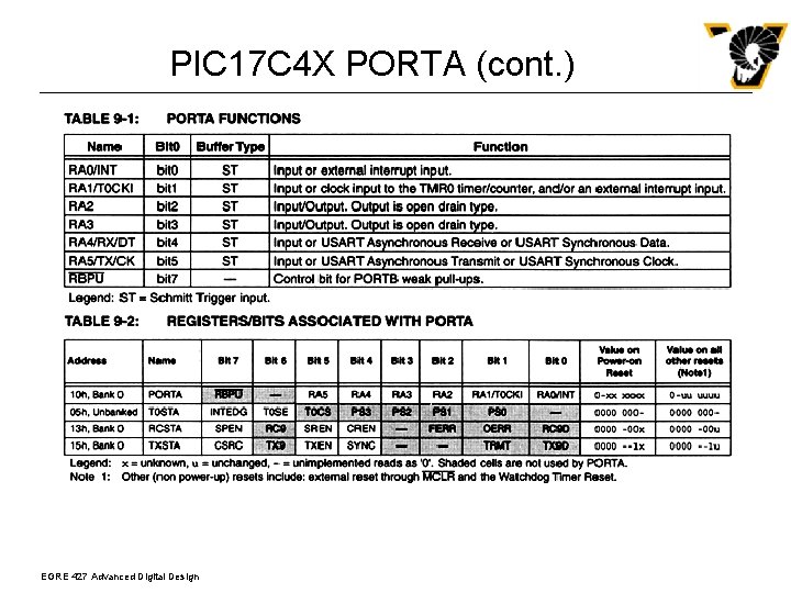
PIC 17 C 4 X PORTA l PORTA does not have a DDR l RA 0/INT is either a data input or external interrupt input l RA 1/T 0 CKI is either a data input, the TMR 0 external clock, or an external interrupt input l RA 2, RA 3 are open drain outputs - simply write to PORTA register to output values to them, the other PORTA pins are unaffected l RA 4, RA 5 are either inputs or USART pins - they are automatically configured by the USART module if it is active l Bit 7 of the PORTA register controls the weak pull-up resistors for PORTB EGRE 427 Advanced Digital Design

PIC 17 C 4 X PORTA (cont. ) EGRE 427 Advanced Digital Design

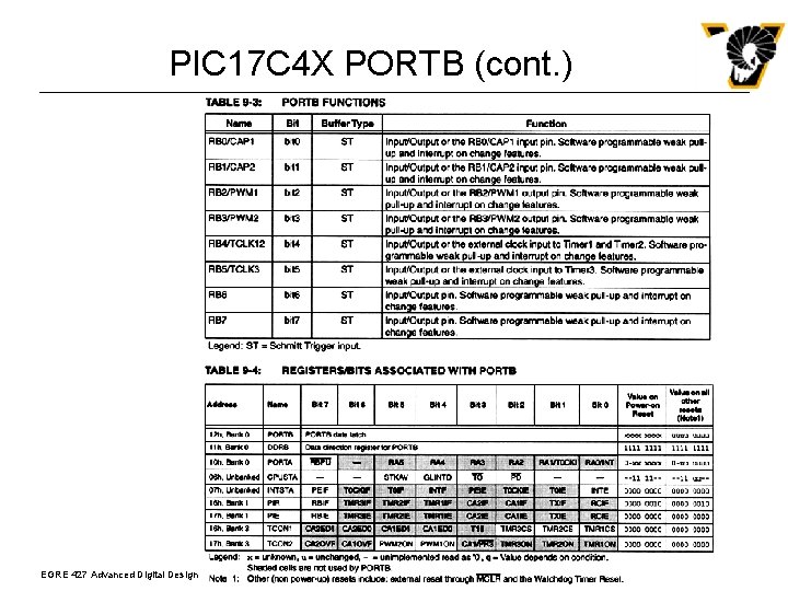
PIC 17 C 4 X PORTB l l PORTB is an 8 -bit wide bi-directional port The corresponding data direction register is DDRB n n l l A ‘ 1’ in the bit of DDRB configures the pin as an input A ‘ 0’ in the bit of DDRB configures the pin as an output Reading PORTB reads the status of the pins - writing PORTB writes to the port latch Each pin of PORTB has a weak internal pull-up resistor enabled by clearing RBPU The weak pull-ups are enabled on reset and automatically turned off when a pin is configured as an output PORTB has an interrupt on change feature n n n Only pins configured as inputs cause this interrupt to occur Input values are compared with the value in the PORTB data latch - any mismatch causes the interrupt This interrupt can wake the processor from the SLEEP mode EGRE 427 Advanced Digital Design

PIC 17 C 4 X PORTB (cont. ) EGRE 427 Advanced Digital Design

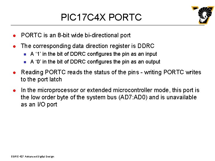
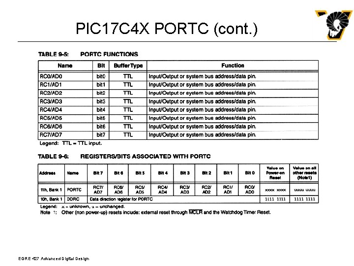
PIC 17 C 4 X PORTC l PORTC is an 8 -bit wide bi-directional port l The corresponding data direction register is DDRC n n A ‘ 1’ in the bit of DDRC configures the pin as an input A ‘ 0’ in the bit of DDRC configures the pin as an output l Reading PORTC reads the status of the pins - writing PORTC writes to the port latch l In the microprocessor or extended microcontroller mode, this port is the low order byte of the system bus (AD 7: AD 0) and is unavailable as an I/O port EGRE 427 Advanced Digital Design

PIC 17 C 4 X PORTC (cont. ) EGRE 427 Advanced Digital Design

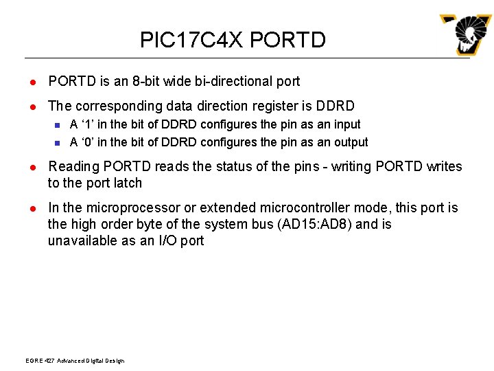
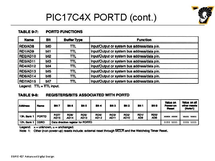
PIC 17 C 4 X PORTD l PORTD is an 8 -bit wide bi-directional port l The corresponding data direction register is DDRD n n A ‘ 1’ in the bit of DDRD configures the pin as an input A ‘ 0’ in the bit of DDRD configures the pin as an output l Reading PORTD reads the status of the pins - writing PORTD writes to the port latch l In the microprocessor or extended microcontroller mode, this port is the high order byte of the system bus (AD 15: AD 8) and is unavailable as an I/O port EGRE 427 Advanced Digital Design

PIC 17 C 4 X PORTD (cont. ) EGRE 427 Advanced Digital Design

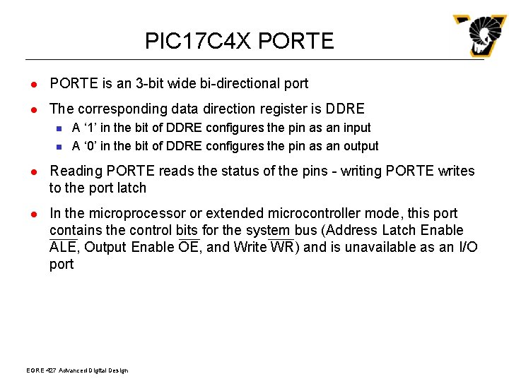
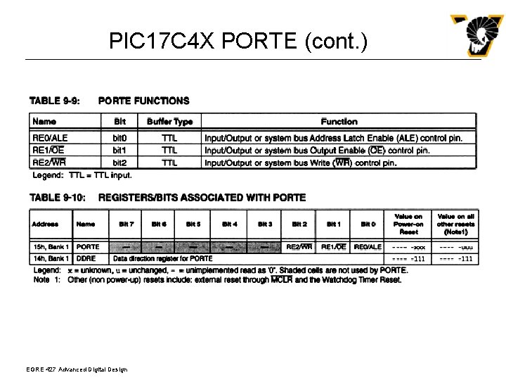
PIC 17 C 4 X PORTE l PORTE is an 3 -bit wide bi-directional port l The corresponding data direction register is DDRE n n A ‘ 1’ in the bit of DDRE configures the pin as an input A ‘ 0’ in the bit of DDRE configures the pin as an output l Reading PORTE reads the status of the pins - writing PORTE writes to the port latch l In the microprocessor or extended microcontroller mode, this port contains the control bits for the system bus (Address Latch Enable ALE, Output Enable OE, and Write WR) and is unavailable as an I/O port EGRE 427 Advanced Digital Design

PIC 17 C 4 X PORTE (cont. ) EGRE 427 Advanced Digital Design

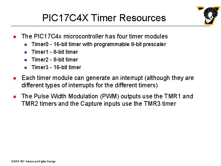
PIC 17 C 4 X Timer Resources l The PIC 17 C 4 x microcontroller has four timer modules n n Timer 0 - 16 -bit timer with programmable 8 -bit prescaler Timer 1 - 8 -bit timer Timer 2 - 8 -bit timer Timer 3 - 16 -bit timer l Each timer module can generate an interrupt (although they are different types of interrupts for the different timers) l The Pulse Width Modulation (PWM) outputs use the TMR 1 and TMR 2 timers and the Capture inputs use the TMR 3 timer EGRE 427 Advanced Digital Design

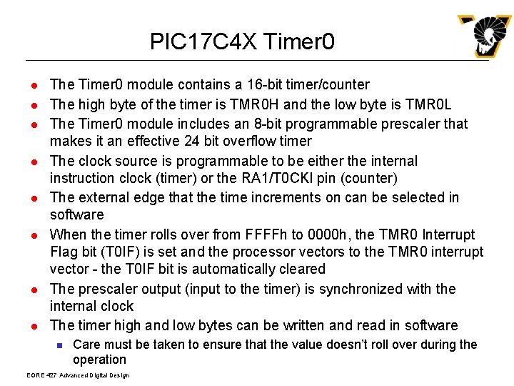
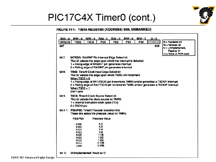
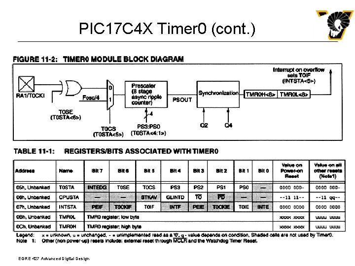
PIC 17 C 4 X Timer 0 l l l l The Timer 0 module contains a 16 -bit timer/counter The high byte of the timer is TMR 0 H and the low byte is TMR 0 L The Timer 0 module includes an 8 -bit programmable prescaler that makes it an effective 24 bit overflow timer The clock source is programmable to be either the internal instruction clock (timer) or the RA 1/T 0 CKI pin (counter) The external edge that the time increments on can be selected in software When the timer rolls over from FFFFh to 0000 h, the TMR 0 Interrupt Flag bit (T 0 IF) is set and the processor vectors to the TMR 0 interrupt vector - the T 0 IF bit is automatically cleared The prescaler output (input to the timer) is synchronized with the internal clock The timer high and low bytes can be written and read in software n Care must be taken to ensure that the value doesn’t roll over during the operation EGRE 427 Advanced Digital Design

PIC 17 C 4 X Timer 0 (cont. ) EGRE 427 Advanced Digital Design

PIC 17 C 4 X Timer 0 (cont. ) EGRE 427 Advanced Digital Design

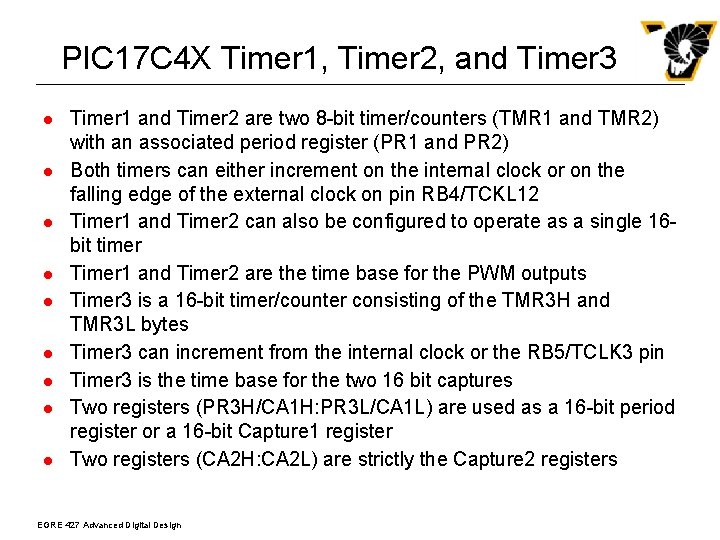
PIC 17 C 4 X Timer 1, Timer 2, and Timer 3 l l l l l Timer 1 and Timer 2 are two 8 -bit timer/counters (TMR 1 and TMR 2) with an associated period register (PR 1 and PR 2) Both timers can either increment on the internal clock or on the falling edge of the external clock on pin RB 4/TCKL 12 Timer 1 and Timer 2 can also be configured to operate as a single 16 bit timer Timer 1 and Timer 2 are the time base for the PWM outputs Timer 3 is a 16 -bit timer/counter consisting of the TMR 3 H and TMR 3 L bytes Timer 3 can increment from the internal clock or the RB 5/TCLK 3 pin Timer 3 is the time base for the two 16 bit captures Two registers (PR 3 H/CA 1 H: PR 3 L/CA 1 L) are used as a 16 -bit period register or a 16 -bit Capture 1 register Two registers (CA 2 H: CA 2 L) are strictly the Capture 2 registers EGRE 427 Advanced Digital Design

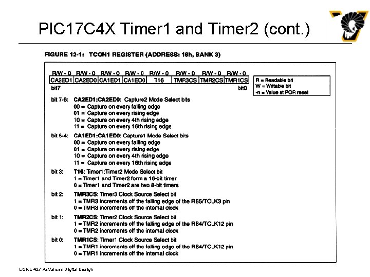
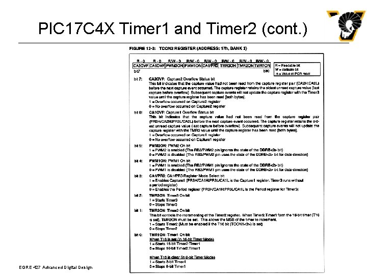
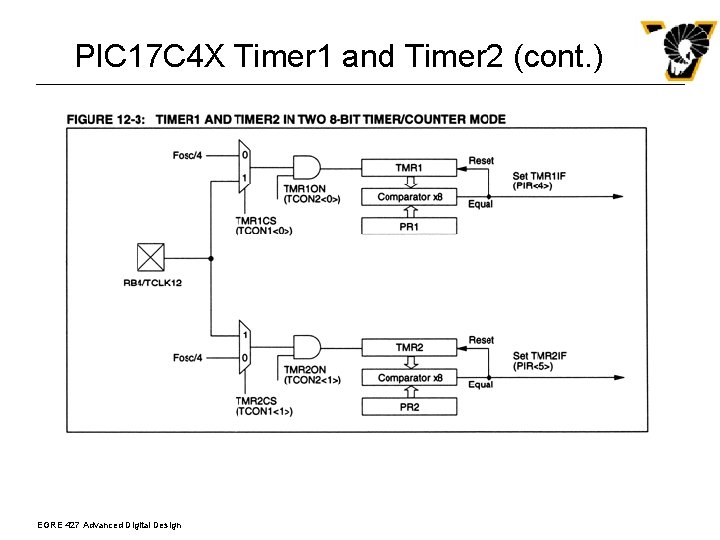
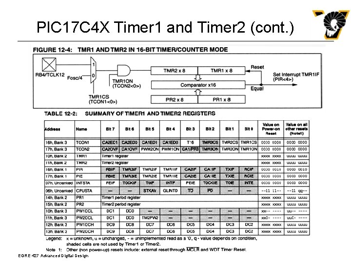
PIC 17 C 4 X Timer 1 and Timer 2 l l l Timer 1 and Timer 2 operate in 8 -bit mode when the T 16 bit is clear Their clocks can be independently selected to be either internal or an external falling edge (RB 4/TCLK 12) The timers increment from 00 h until they equal the period register (PRx) and then reset in the next cycle The timer interrupt flag (TMR 1 F and TMR 2 F flag is set when the timer rolls over (and their individual interrupts are enabled) The Timer 1 and Timer 2 interrupts are peripheral interrupts n n n l l l Peripheral interrupts as well as the individual timer interrupts must be enabled The PIR register must be checked to determine the source of interrupts The individual timer interrupt flags must be cleared in software When the T 16 bit is set Timer 1 and Timer 2 form a 16 -bit timer/counter The timer counts from 0000 h until it equals the period register (PR 2: PR 1) The TMR 1 CS bit controls the clock source for the 16 -bit timer EGRE 427 Advanced Digital Design

PIC 17 C 4 X Timer 1 and Timer 2 (cont. ) EGRE 427 Advanced Digital Design

PIC 17 C 4 X Timer 1 and Timer 2 (cont. ) EGRE 427 Advanced Digital Design

PIC 17 C 4 X Timer 1 and Timer 2 (cont. ) EGRE 427 Advanced Digital Design

PIC 17 C 4 X Timer 1 and Timer 2 (cont. ) EGRE 427 Advanced Digital Design

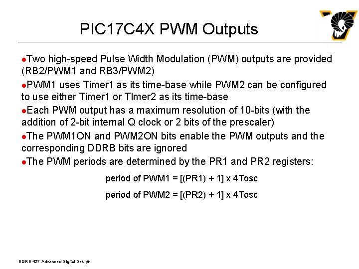
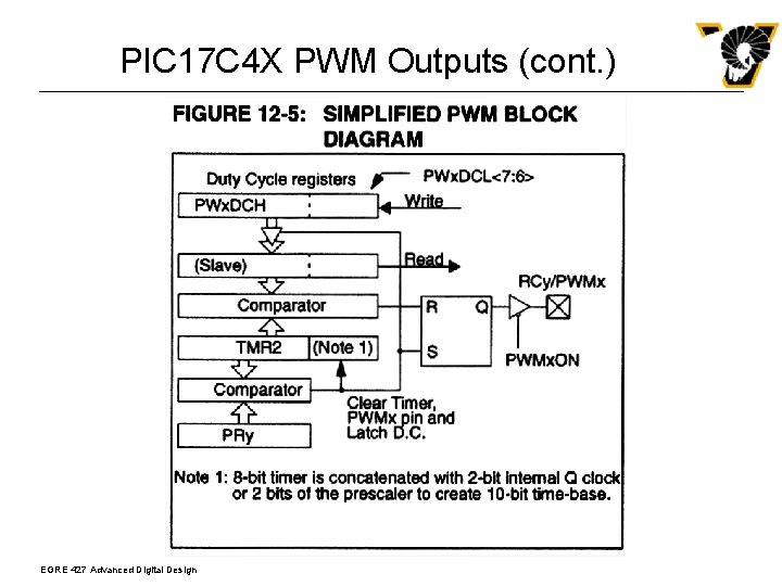
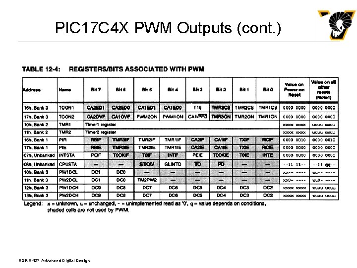
PIC 17 C 4 X PWM Outputs l. Two high-speed Pulse Width Modulation (PWM) outputs are provided (RB 2/PWM 1 and RB 3/PWM 2) l. PWM 1 uses Timer 1 as its time-base while PWM 2 can be configured to use either Timer 1 or TImer 2 as its time-base l. Each PWM output has a maximum resolution of 10 -bits (with the addition of 2 -bit internal Q clock or 2 bits of the prescaler) l. The PWM 1 ON and PWM 2 ON bits enable the PWM outputs and the corresponding DDRB bits are ignored l. The PWM periods are determined by the PR 1 and PR 2 registers: period of PWM 1 = [(PR 1) + 1] x 4 Tosc period of PWM 2 = [(PR 2) + 1] x 4 Tosc EGRE 427 Advanced Digital Design

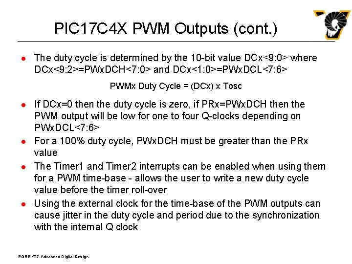
PIC 17 C 4 X PWM Outputs (cont. ) l The duty cycle is determined by the 10 -bit value DCx<9: 0> where DCx<9: 2>=PWx. DCH<7: 0> and DCx<1: 0>=PWx. DCL<7: 6> PWMx Duty Cycle = (DCx) x Tosc l l If DCx=0 then the duty cycle is zero, if PRx=PWx. DCH then the PWM output will be low for one to four Q-clocks depending on PWx. DCL<7: 6> For a 100% duty cycle, PWx. DCH must be greater than the PRx value The Timer 1 and Timer 2 interrupts can be enabled when using them for a PWM time-base - allows the user to write a new duty cycle value before the timer roll-over Using the external clock for the time-base of the PWM outputs can cause jitter in the duty cycle and period due to the synchronization with the internal Q clock EGRE 427 Advanced Digital Design

PIC 17 C 4 X PWM Outputs (cont. ) EGRE 427 Advanced Digital Design

PIC 17 C 4 X PWM Outputs (cont. ) EGRE 427 Advanced Digital Design

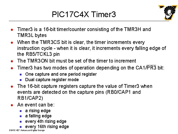
PIC 17 C 4 X Timer 3 l l Timer 3 is a 16 -bit timer/counter consisting of the TMR 3 H and TMR 3 L bytes When the TMR 3 CS bit is clear, the timer increments every instruction cycle - when it is clear, it increments every falling edge of the RB 5/TCKL 3 pin The TMR 3 ON bit must be set of the timer to increment Timer 3 has two modes of operation depending on the CA 1/PR 3 bit: n n l l One capture and one period register Dual capture register mode The 16 -bit capture registers capture the value of Timer 3 when events are detected on the capture pins (RB 0/CAP 1 and RB 1/CAP 2) An event can be: n n a rising edge a falling edge every 4 th rising edge every 16 th rising edge EGRE 427 Advanced Digital Design

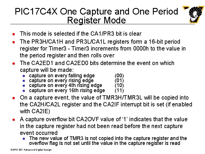
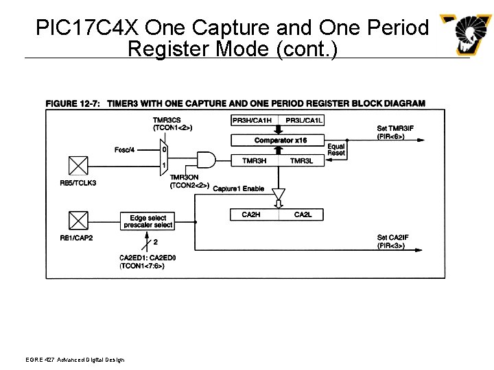
PIC 17 C 4 X One Capture and One Period Register Mode l l l This mode is selected if the CA 1/PR 3 bit is clear The PR 3 H/CA 1 H and PR 3 L/CA 1 L registers form a 16 -bit period register for Timer 3 - Timer 3 increments from 0000 h to the value in the period register and then rolls over The CA 2 ED 1 and CA 2 ED 0 bits determine the event on which capture will be made: n n l l capture on every falling edge capture on every rising edge capture on every 4 th rising edge capture on every 16 th rising edge (00) (01) (10) (11) On a capture event, the value of TMR 3 H/TMR 3 L will be copied into the CA 2 H/CA 2 L register and the CA 2 IF interrupt bit is set (if enabled with CA 2 IE) A capture overflow bit CA 2 OVF value of ‘ 1’ indicates that the value in the capture register had not been read before the next capture event occurred n The new value of TMR 3 is not copied into the capture register and the overflow flag is not set until the value in the capture register is read EGRE 427 Advanced Digital Design

PIC 17 C 4 X One Capture and One Period Register Mode (cont. ) EGRE 427 Advanced Digital Design

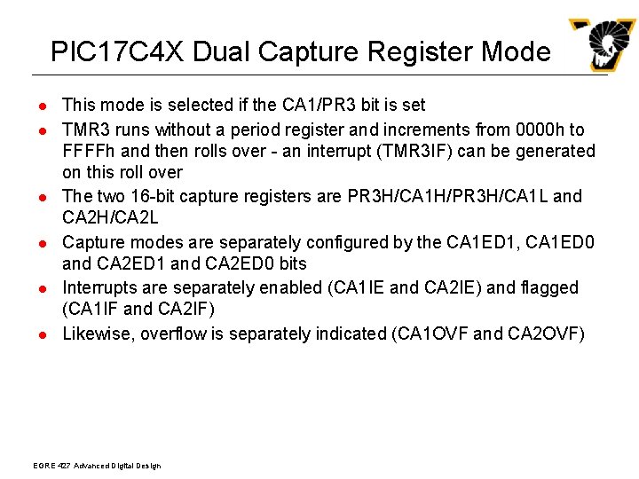
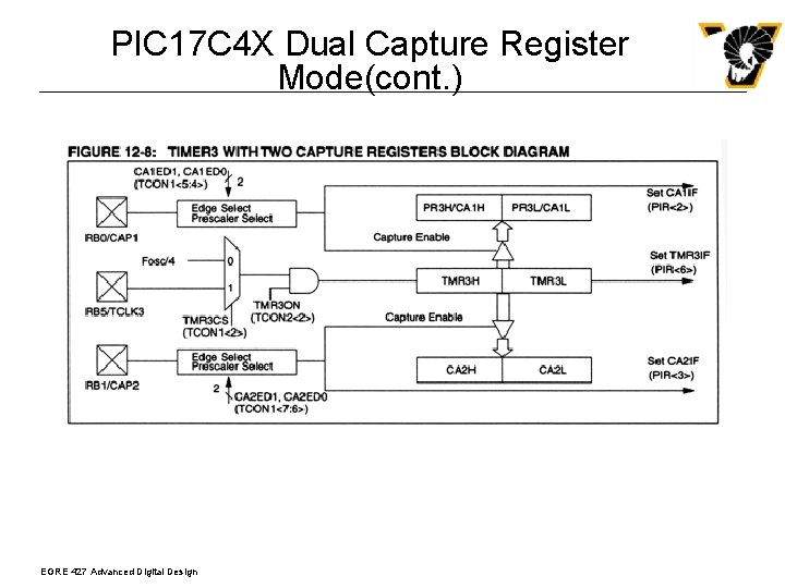
PIC 17 C 4 X Dual Capture Register Mode l l l This mode is selected if the CA 1/PR 3 bit is set TMR 3 runs without a period register and increments from 0000 h to FFFFh and then rolls over - an interrupt (TMR 3 IF) can be generated on this roll over The two 16 -bit capture registers are PR 3 H/CA 1 H/PR 3 H/CA 1 L and CA 2 H/CA 2 L Capture modes are separately configured by the CA 1 ED 1, CA 1 ED 0 and CA 2 ED 1 and CA 2 ED 0 bits Interrupts are separately enabled (CA 1 IE and CA 2 IE) and flagged (CA 1 IF and CA 2 IF) Likewise, overflow is separately indicated (CA 1 OVF and CA 2 OVF) EGRE 427 Advanced Digital Design

PIC 17 C 4 X Dual Capture Register Mode(cont. ) EGRE 427 Advanced Digital Design

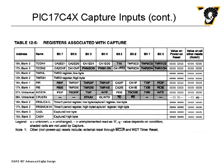
PIC 17 C 4 X Capture Inputs (cont. ) EGRE 427 Advanced Digital Design

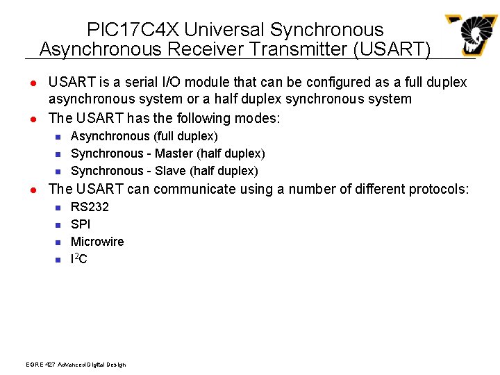
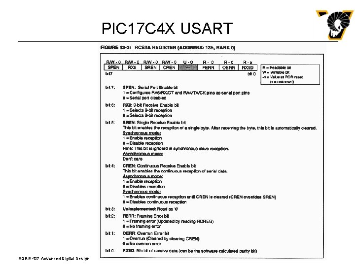
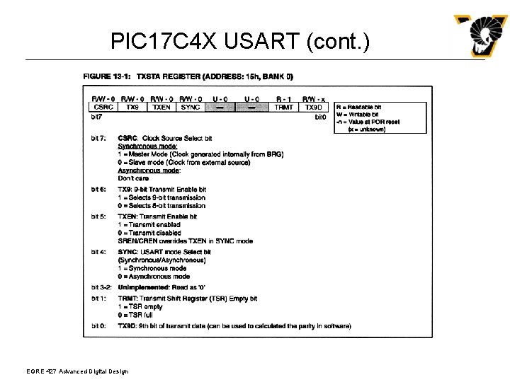
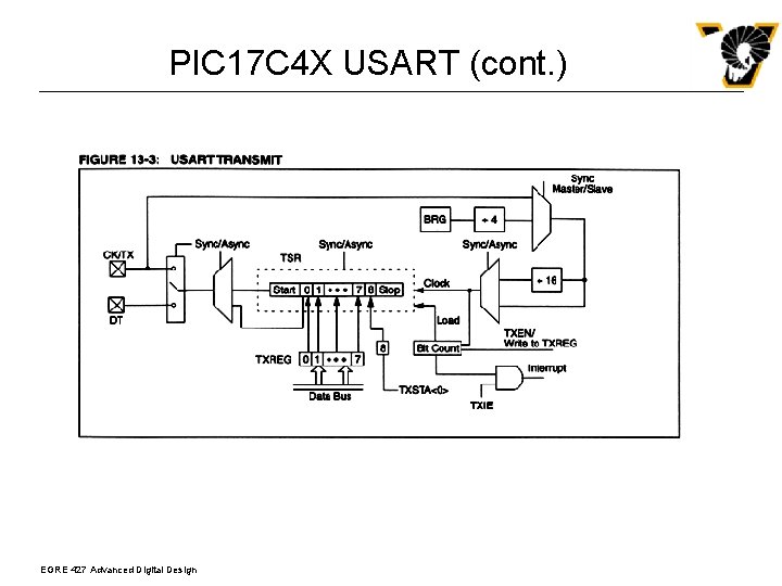
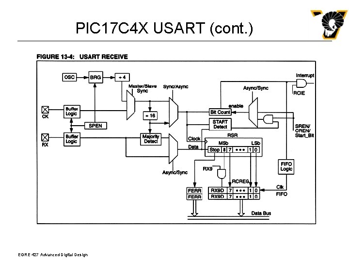
PIC 17 C 4 X Universal Synchronous Asynchronous Receiver Transmitter (USART) l l USART is a serial I/O module that can be configured as a full duplex asynchronous system or a half duplex synchronous system The USART has the following modes: n n n l Asynchronous (full duplex) Synchronous - Master (half duplex) Synchronous - Slave (half duplex) The USART can communicate using a number of different protocols: n n RS 232 SPI Microwire I 2 C EGRE 427 Advanced Digital Design

PIC 17 C 4 X USART EGRE 427 Advanced Digital Design

PIC 17 C 4 X USART (cont. ) EGRE 427 Advanced Digital Design

PIC 17 C 4 X USART (cont. ) EGRE 427 Advanced Digital Design

PIC 17 C 4 X USART (cont. ) EGRE 427 Advanced Digital Design

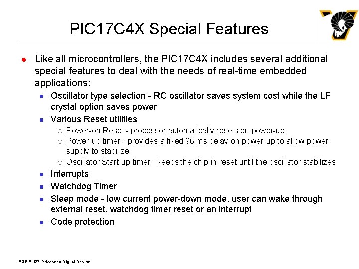
PIC 17 C 4 X Special Features l Like all microcontrollers, the PIC 17 C 4 X includes several additional special features to deal with the needs of real-time embedded applications: n n Oscillator type selection - RC oscillator saves system cost while the LF crystal option saves power Various Reset utilities ¦ ¦ ¦ n n Power-on Reset - processor automatically resets on power-up Power-up timer - provides a fixed 96 ms delay on power-up to allow power supply to stabilize Oscillator Start-up timer - keeps the chip in reset until the oscillator stabilizes Interrupts Watchdog Timer Sleep mode - low current power-down mode, user can wake through external reset, watchdog timer reset or an interrupt Code protection EGRE 427 Advanced Digital Design

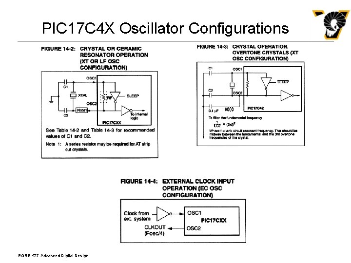
PIC 17 C 4 X Oscillator Configurations EGRE 427 Advanced Digital Design

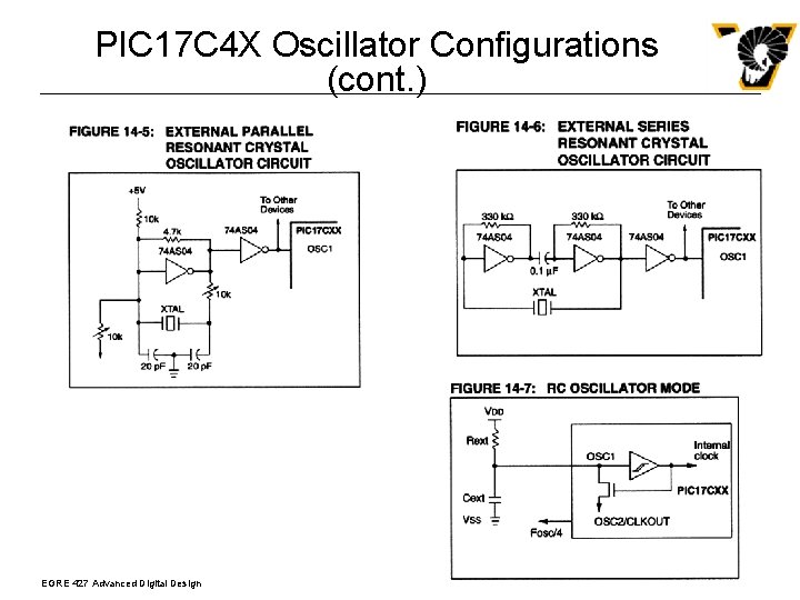
PIC 17 C 4 X Oscillator Configurations (cont. ) EGRE 427 Advanced Digital Design

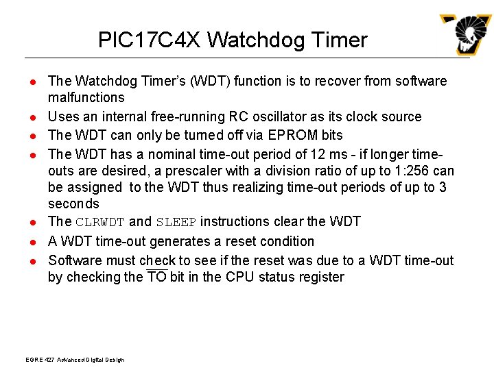
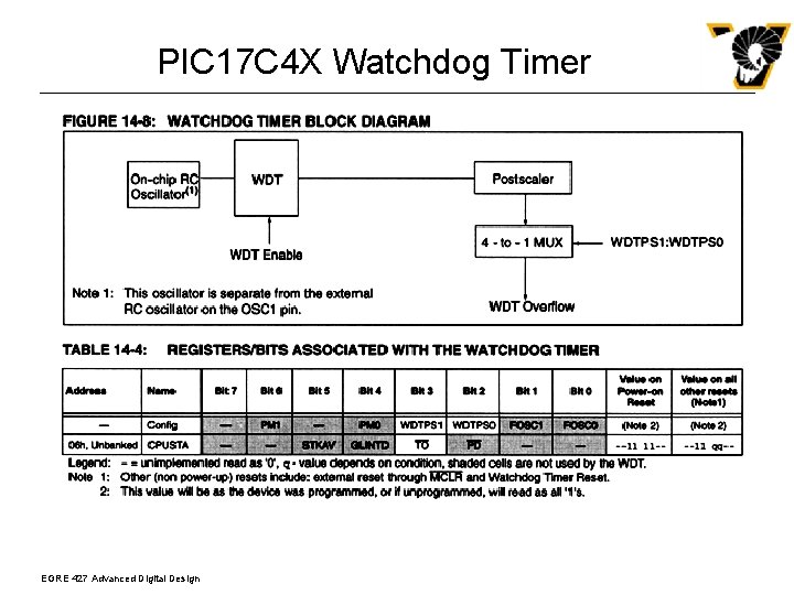
PIC 17 C 4 X Watchdog Timer l l l l The Watchdog Timer’s (WDT) function is to recover from software malfunctions Uses an internal free-running RC oscillator as its clock source The WDT can only be turned off via EPROM bits The WDT has a nominal time-out period of 12 ms - if longer timeouts are desired, a prescaler with a division ratio of up to 1: 256 can be assigned to the WDT thus realizing time-out periods of up to 3 seconds The CLRWDT and SLEEP instructions clear the WDT A WDT time-out generates a reset condition Software must check to see if the reset was due to a WDT time-out by checking the TO bit in the CPU status register EGRE 427 Advanced Digital Design

PIC 17 C 4 X Watchdog Timer EGRE 427 Advanced Digital Design

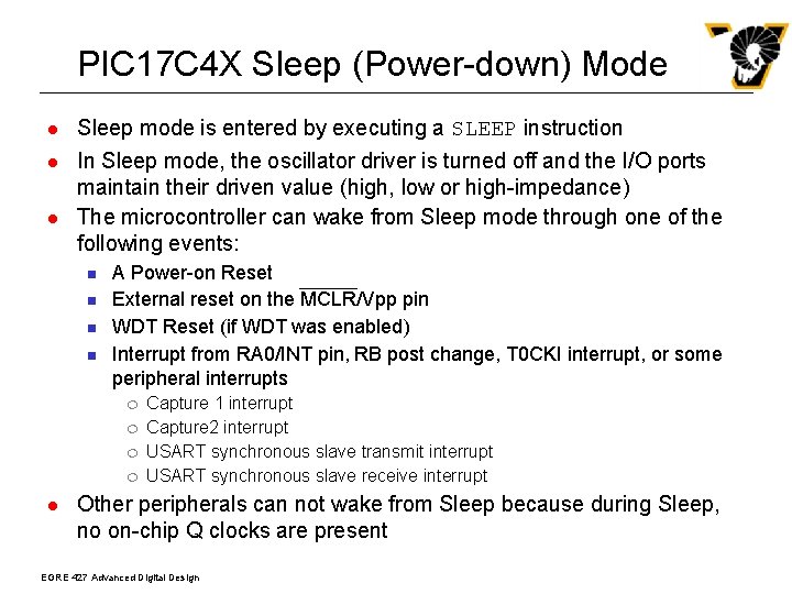
PIC 17 C 4 X Sleep (Power-down) Mode l l l Sleep mode is entered by executing a SLEEP instruction In Sleep mode, the oscillator driver is turned off and the I/O ports maintain their driven value (high, low or high-impedance) The microcontroller can wake from Sleep mode through one of the following events: n n A Power-on Reset External reset on the MCLR/Vpp pin WDT Reset (if WDT was enabled) Interrupt from RA 0/INT pin, RB post change, T 0 CKI interrupt, or some peripheral interrupts ¦ ¦ l Capture 1 interrupt Capture 2 interrupt USART synchronous slave transmit interrupt USART synchronous slave receive interrupt Other peripherals can not wake from Sleep because during Sleep, no on-chip Q clocks are present EGRE 427 Advanced Digital Design

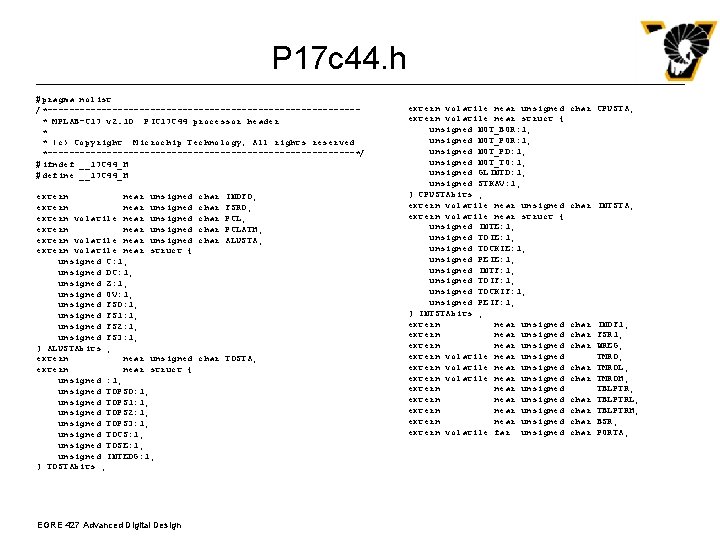
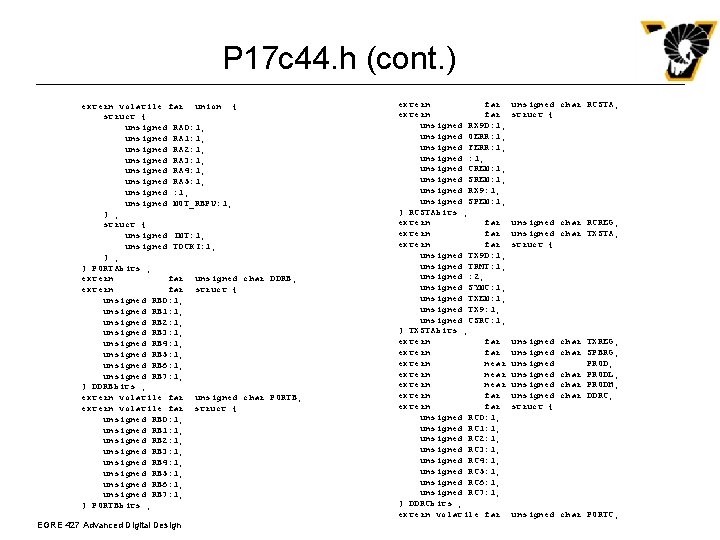
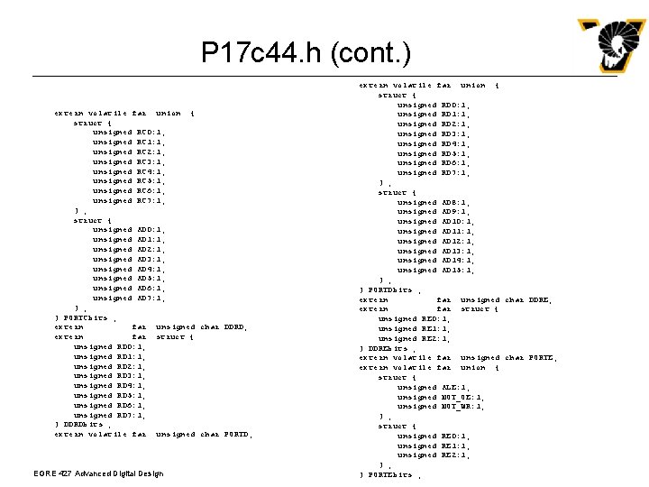
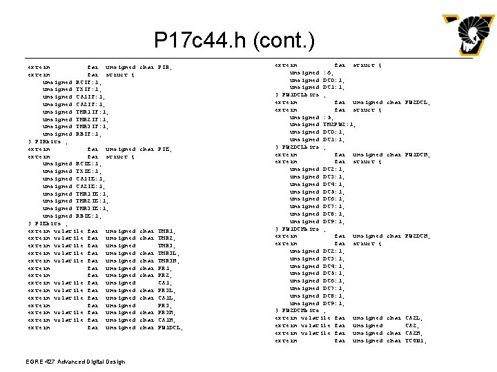
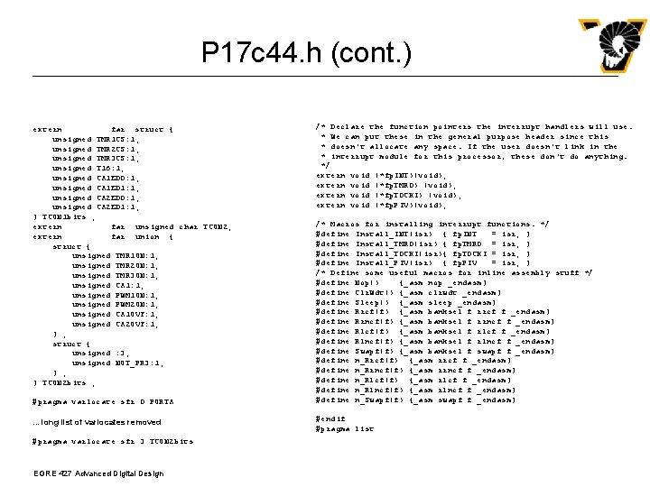
Programming the PIC 17 C 4 X in “C” l l The Microchip development environment includes a compiler for the “C” programming language Included with the compiler a libraries for manipulating the special functions of the PIC microcontrollers These libraries consist of header files which define the registers and variables necessary and C functions which perform some of the needed actions The main header file for each processor defines the all of the registers and individual bits that have been discussed - thus it is always possible for you to manipulate the hardware registers and setup the functions directly EGRE 427 Advanced Digital Design

P 17 c 44. h #pragma nolist /*-----------------------------* MPLAB-C 17 v 2. 10 PIC 17 C 44 processor header * * (c) Copyright Microchip Technology, All rights reserved *-----------------------------*/ #ifndef __17 C 44_H #define __17 C 44_H extern near unsigned extern volatile near unsigned extern volatile near struct { unsigned C: 1; unsigned DC: 1; unsigned Z: 1; unsigned OV: 1; unsigned FS 0: 1; unsigned FS 1: 1; unsigned FS 2: 1; unsigned FS 3: 1; } ALUSTAbits ; extern near unsigned extern near struct { unsigned : 1; unsigned T 0 PS 0: 1; unsigned T 0 PS 1: 1; unsigned T 0 PS 2: 1; unsigned T 0 PS 3: 1; unsigned T 0 CS: 1; unsigned T 0 SE: 1; unsigned INTEDG: 1; } T 0 STAbits ; EGRE 427 Advanced Digital Design char char INDF 0; FSR 0; PCLATH; ALUSTA; char T 0 STA; extern volatile near unsigned extern volatile near struct { unsigned NOT_BOR: 1; unsigned NOT_PD: 1; unsigned NOT_TO: 1; unsigned GLINTD: 1; unsigned STKAV: 1; } CPUSTAbits ; extern volatile near unsigned extern volatile near struct { unsigned INTE: 1; unsigned T 0 IE: 1; unsigned T 0 CKIE: 1; unsigned PEIE: 1; unsigned INTF: 1; unsigned T 0 IF: 1; unsigned T 0 CKIF: 1; unsigned PEIF: 1; } INTSTAbits ; extern near unsigned extern volatile near unsigned extern near unsigned extern volatile far unsigned char CPUSTA; char INTSTA; char INDF 1; char FSR 1; char WREG; TMR 0; char TMR 0 L; char TMR 0 H; TBLPTR; char TBLPTRL; char TBLPTRH; char BSR; char PORTA;

P 17 c 44. h (cont. ) extern volatile far union { struct { unsigned RA 0: 1; unsigned RA 1: 1; unsigned RA 2: 1; unsigned RA 3: 1; unsigned RA 4: 1; unsigned RA 5: 1; unsigned NOT_RBPU: 1; } ; struct { unsigned INT: 1; unsigned T 0 CKI: 1; } PORTAbits ; extern far unsigned char DDRB; extern far struct { unsigned RB 0: 1; unsigned RB 1: 1; unsigned RB 2: 1; unsigned RB 3: 1; unsigned RB 4: 1; unsigned RB 5: 1; unsigned RB 6: 1; unsigned RB 7: 1; } DDRBbits ; extern volatile far unsigned char PORTB; extern volatile far struct { unsigned RB 0: 1; unsigned RB 1: 1; unsigned RB 2: 1; unsigned RB 3: 1; unsigned RB 4: 1; unsigned RB 5: 1; unsigned RB 6: 1; unsigned RB 7: 1; } PORTBbits ; EGRE 427 Advanced Digital Design extern far unsigned RX 9 D: 1; unsigned OERR: 1; unsigned FERR: 1; unsigned CREN: 1; unsigned SREN: 1; unsigned RX 9: 1; unsigned SPEN: 1; } RCSTAbits ; extern far unsigned TX 9 D: 1; unsigned TRMT: 1; unsigned : 2; unsigned SYNC: 1; unsigned TXEN: 1; unsigned TX 9: 1; unsigned CSRC: 1; } TXSTAbits ; extern far extern near extern far unsigned RC 0: 1; unsigned RC 1: 1; unsigned RC 2: 1; unsigned RC 3: 1; unsigned RC 4: 1; unsigned RC 5: 1; unsigned RC 6: 1; unsigned RC 7: 1; } DDRCbits ; extern volatile far unsigned char RCSTA; struct { unsigned char RCREG; unsigned char TXSTA; struct { unsigned unsigned struct { char TXREG; char SPBRG; PROD; char PRODL; char PRODH; char DDRC; unsigned char PORTC;

P 17 c 44. h (cont. ) extern volatile far union { struct { unsigned RC 0: 1; unsigned RC 1: 1; unsigned RC 2: 1; unsigned RC 3: 1; unsigned RC 4: 1; unsigned RC 5: 1; unsigned RC 6: 1; unsigned RC 7: 1; } ; struct { unsigned AD 0: 1; unsigned AD 1: 1; unsigned AD 2: 1; unsigned AD 3: 1; unsigned AD 4: 1; unsigned AD 5: 1; unsigned AD 6: 1; unsigned AD 7: 1; } PORTCbits ; extern far unsigned char DDRD; extern far struct { unsigned RD 0: 1; unsigned RD 1: 1; unsigned RD 2: 1; unsigned RD 3: 1; unsigned RD 4: 1; unsigned RD 5: 1; unsigned RD 6: 1; unsigned RD 7: 1; } DDRDbits ; extern volatile far unsigned char PORTD; EGRE 427 Advanced Digital Design extern volatile far union { struct { unsigned RD 0: 1; unsigned RD 1: 1; unsigned RD 2: 1; unsigned RD 3: 1; unsigned RD 4: 1; unsigned RD 5: 1; unsigned RD 6: 1; unsigned RD 7: 1; } ; struct { unsigned AD 8: 1; unsigned AD 9: 1; unsigned AD 10: 1; unsigned AD 11: 1; unsigned AD 12: 1; unsigned AD 13: 1; unsigned AD 14: 1; unsigned AD 15: 1; } PORTDbits ; extern far unsigned char DDRE; extern far struct { unsigned RE 0: 1; unsigned RE 1: 1; unsigned RE 2: 1; } DDREbits ; extern volatile far unsigned char PORTE; extern volatile far union { struct { unsigned ALE: 1; unsigned NOT_OE: 1; unsigned NOT_WR: 1; } ; struct { unsigned RE 0: 1; unsigned RE 1: 1; unsigned RE 2: 1; } PORTEbits ;

P 17 c 44. h (cont. ) extern far unsigned extern far struct { unsigned RCIF: 1; unsigned TXIF: 1; unsigned CA 1 IF: 1; unsigned CA 2 IF: 1; unsigned TMR 1 IF: 1; unsigned TMR 2 IF: 1; unsigned TMR 3 IF: 1; unsigned RBIF: 1; } PIRbits ; extern far unsigned extern far struct { unsigned RCIE: 1; unsigned TXIE: 1; unsigned CA 1 IE: 1; unsigned CA 2 IE: 1; unsigned TMR 1 IE: 1; unsigned TMR 2 IE: 1; unsigned TMR 3 IE: 1; unsigned RBIE: 1; } PIEbits ; extern volatile far unsigned extern volatile far unsigned extern volatile far unsigned extern far unsigned EGRE 427 Advanced Digital Design char PIR; char PIE; char TMR 1; char TMR 2; TMR 3; char TMR 3 L; char TMR 3 H; char PR 1; char PR 2; CA 1; char PR 3 L; char CA 1 L; PR 3; char PR 3 H; char CA 1 H; char PW 1 DCL; extern far struct { unsigned : 6; unsigned DC 0: 1; unsigned DC 1: 1; } PW 1 DCLbits ; extern far unsigned extern far struct { unsigned : 5; unsigned TM 2 PW 2: 1; unsigned DC 0: 1; unsigned DC 1: 1; } PW 2 DCLbits ; extern far unsigned extern far struct { unsigned DC 2: 1; unsigned DC 3: 1; unsigned DC 4: 1; unsigned DC 5: 1; unsigned DC 6: 1; unsigned DC 7: 1; unsigned DC 8: 1; unsigned DC 9: 1; } PW 1 DCHbits ; extern far unsigned extern far struct { unsigned DC 2: 1; unsigned DC 3: 1; unsigned DC 4: 1; unsigned DC 5: 1; unsigned DC 6: 1; unsigned DC 7: 1; unsigned DC 8: 1; unsigned DC 9: 1; } PW 2 DCHbits ; extern volatile far unsigned extern far unsigned char PW 2 DCL; char PW 1 DCH; char PW 2 DCH; char CA 2 L; CA 2; char CA 2 H; char TCON 1;

P 17 c 44. h (cont. ) extern far struct { unsigned TMR 1 CS: 1; unsigned TMR 2 CS: 1; unsigned TMR 3 CS: 1; unsigned T 16: 1; unsigned CA 1 ED 0: 1; unsigned CA 1 ED 1: 1; unsigned CA 2 ED 0: 1; unsigned CA 2 ED 1: 1; } TCON 1 bits ; extern far unsigned char TCON 2; extern far union { struct { unsigned TMR 1 ON: 1; unsigned TMR 2 ON: 1; unsigned TMR 3 ON: 1; unsigned CA 1: 1; unsigned PWM 1 ON: 1; unsigned PWM 2 ON: 1; unsigned CA 1 OVF: 1; unsigned CA 2 OVF: 1; } ; struct { unsigned : 3; unsigned NOT_PR 3: 1; } TCON 2 bits ; #pragma varlocate sfr 0 PORTA. . . long list of varlocates removed #pragma varlocate sfr 3 TCON 2 bits EGRE 427 Advanced Digital Design /* Declare the function pointers the interrupt handlers will use. * We can put these in the general purpose header since this * doesn't allocate any space. If the user doesn't link in the * interrupt module for this processor, these don't do anything. */ extern void (*fp. INT)(void); extern void (*fp. TMR 0) (void); extern void (*fp. T 0 CKI) (void); extern void (*fp. PIV)(void); /* Macros for installing interrupt functions. */ #define Install_INT(isr) { fp. INT = isr; } #define Install_TMR 0(isr) { fp. TMR 0 = isr; } #define Install_T 0 CKI(isr){ fp. T 0 CKI = isr; } #define Install_PIV(isr) { fp. PIV = isr; } /* Define some useful macros for inline assembly stuff */ #define Nop() {_asm nop _endasm} #define Clr. Wdt() {_asm clrwdt _endasm} #define Sleep() {_asm sleep _endasm} #define Rrcf(f) {_asm banksel f rrcf f _endasm} #define Rrncf(f) {_asm banksel f rrncf f _endasm} #define Rlcf(f) {_asm banksel f rlcf f _endasm} #define Rlncf(f) {_asm banksel f rlncf f _endasm} #define Swapf(f) {_asm banksel f swapf f _endasm} #define n_Rrcf(f) {_asm rrcf f _endasm} #define n_Rrncf(f) {_asm rrncf f _endasm} #define n_Rlcf(f) {_asm rlcf f _endasm} #define n_Rlncf(f) {_asm rlncf f _endasm} #define n_Swapf(f) {_asm swapf f _endasm} #endif #pragma list

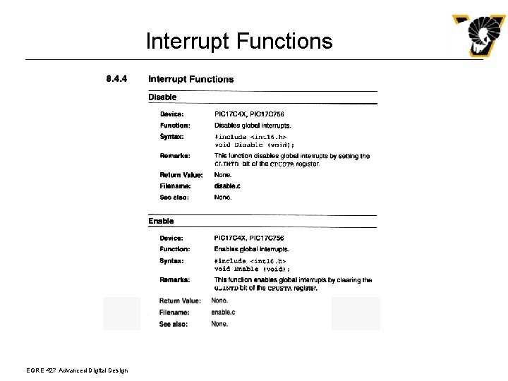
Interrupt Functions EGRE 427 Advanced Digital Design

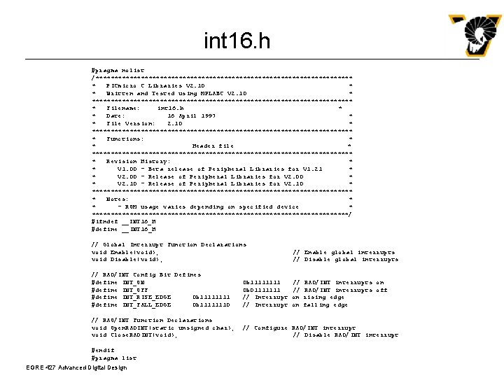
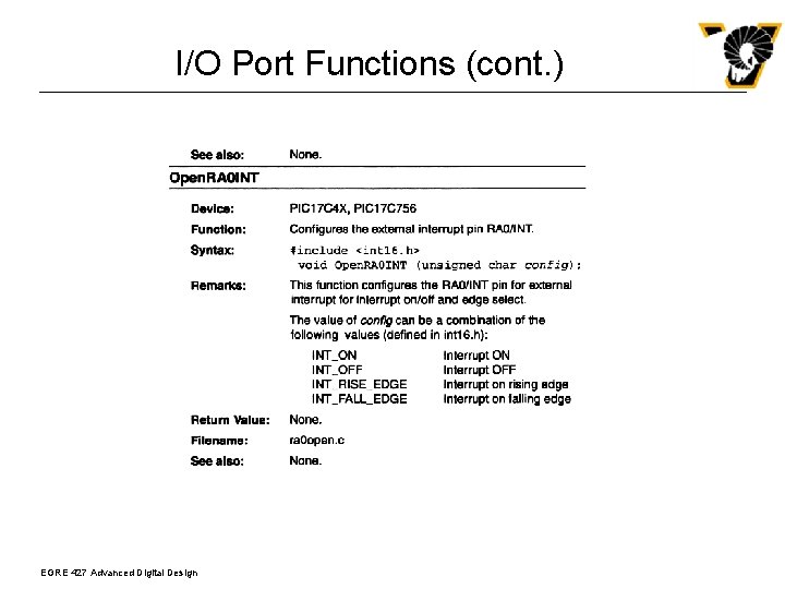
int 16. h #pragma nolist /********************************** * PICmicro C Libraries V 2. 10 * * Written and Tested using MPLABC V 2. 10 * *********************************** * Filename: int 16. h * * Date: 16 April 1997 * * File Version: 2. 10 * *********************************** * Functions: * * Header file * *********************************** * Revision History: * * V 1. 00 - Beta release of Peripheral Libraries for V 1. 21 * * V 2. 00 - Release of Peripheral Libraries for V 2. 00 * * V 2. 10 - Release of Peripheral Libraries for V 2. 10 * *********************************** * Notes: * * - ROM usage varies depending on specified device * **********************************/ #ifndef __INT 16_H #define __INT 16_H // Global Interrupt Function Declarations void Enable(void); void Disable(void); // Enable global interrupts // Disable global interrupts // RA 0/INT Config Bit Defines #define INT_ON #define INT_OFF #define INT_RISE_EDGE 0 b 1111 #define INT_FALL_EDGE 0 b 11111110 0 b 1111 0 b 01111111 // Interrupt // // on on // RAO/INT Function Declarations void Open. RA 0 INT(static unsigned char); void Close. RA 0 INT(void); // Configure RA 0/INT interrupt // Disable RA 0/INT interrupt #endif #pragma list EGRE 427 Advanced Digital Design RA 0/INT interrupts off rising edge falling edge

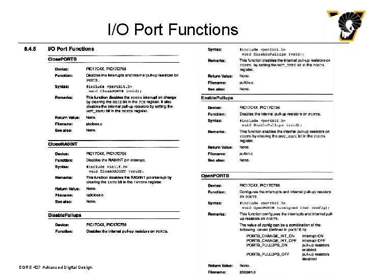
I/O Port Functions EGRE 427 Advanced Digital Design

I/O Port Functions (cont. ) EGRE 427 Advanced Digital Design

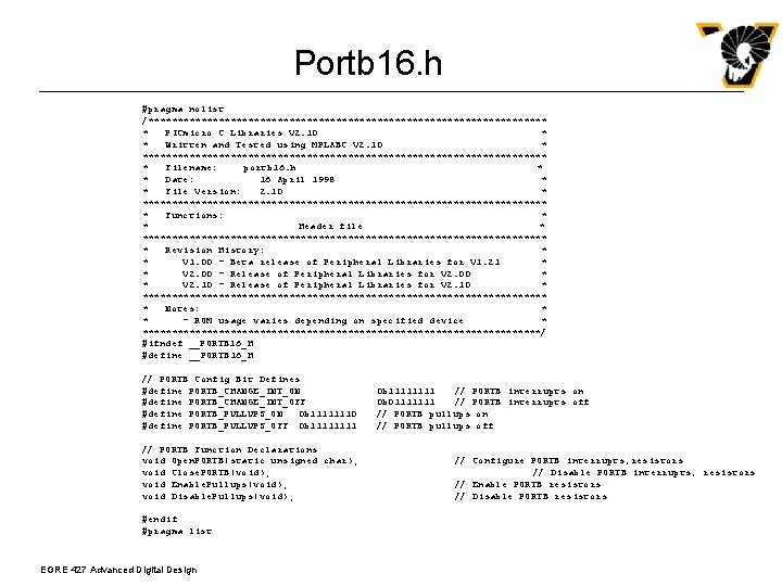
Portb 16. h #pragma nolist /********************************** * PICmicro C Libraries V 2. 10 * * Written and Tested using MPLABC V 2. 10 * *********************************** * Filename: portb 16. h * * Date: 16 April 1998 * * File Version: 2. 10 * *********************************** * Functions: * * Header file * *********************************** * Revision History: * * V 1. 00 - Beta release of Peripheral Libraries for V 1. 21 * * V 2. 00 - Release of Peripheral Libraries for V 2. 00 * * V 2. 10 - Release of Peripheral Libraries for V 2. 10 * *********************************** * Notes: * * - ROM usage varies depending on specified device * **********************************/ #ifndef __PORTB 16_H #define __PORTB 16_H // PORTB Config Bit Defines #define PORTB_CHANGE_INT_ON #define PORTB_CHANGE_INT_OFF #define PORTB_PULLUPS_ON 0 b 11111110 #define PORTB_PULLUPS_OFF 0 b 1111 // PORTB Function Declarations void Open. PORTB(static unsigned char); void Close. PORTB(void); void Enable. Pullups(void); void Disable. Pullups(void); #endif #pragma list EGRE 427 Advanced Digital Design 0 b 1111 // PORTB interrupts on 0 b 01111111 // PORTB interrupts off // PORTB pullups on // PORTB pullups off // Configure PORTB interrupts, resistors // Disable PORTB interrupts, resistors // Enable PORTB resistors // Disable PORTB resistors

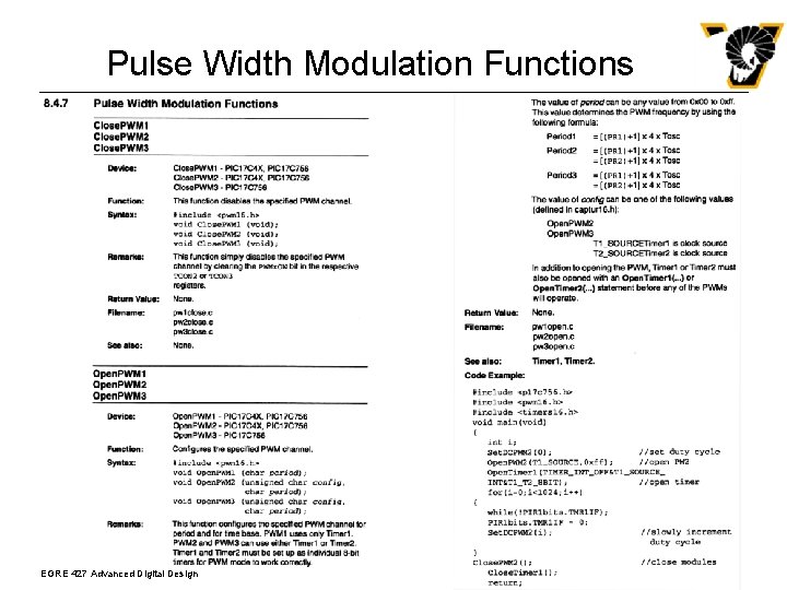
Pulse Width Modulation Functions EGRE 427 Advanced Digital Design

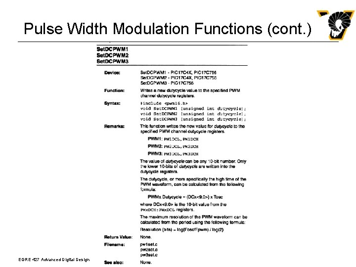
Pulse Width Modulation Functions (cont. ) EGRE 427 Advanced Digital Design

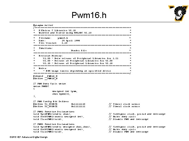
Pwm 16. h #pragma nolist /********************************** * PICmicro C Libraries V 2. 10 * * Written and Tested using MPLABC V 2. 10 * *********************************** * Filename: pwm 16. h * * Date: 14 April 1998 * * File Version: 2. 10 * *********************************** * Functions: * * Header file * *********************************** * Revision History: * * V 1. 00 - Beta release of Peripheral Libraries for 1. 21 * * V 2. 00 - Release of Peripheral Libraries for V 2. 00 * * V 2. 10 - Release of Peripheral Libraries for V 2. 10 * *********************************** * Notes: * * - ROM usage varies depending on specified device * **********************************/ #ifndef __PWM 16_H #define __PWM 16_H // PWM Duty Cycle union PWMDC { unsigned int lpwm; char bpwm[2]; }; // PWM Config Bit Defines #define T 1_SOURCE #define T 2_SOURCE 0 b 11111110 0 b 1111 // Timer 1 clock source // Timer 2 clock source // PWM 1 Function Declarations void Open. PWM 1(static char); void Set. DCPWM 1(static unsigned int); void Close. PWM 1(void); // Configure clock, period and interrupt // Write duty cycle // Disable PWM and interrupt // PWM 2 Function Declarations void Open. PWM 2(static unsigned char, char); void Set. DCPWM 2(static unsigned int); void Close. PWM 2(void); // Configure clock, period and interrupt // Write duty cycle // Disable PWM and interrupt EGRE 427 Advanced Digital Design

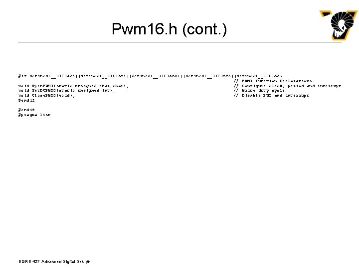
Pwm 16. h (cont. ) #if defined(__17 C 752)||defined(__17 C 756 A)||defined(__17 C 766)||defined(__17 C 762) // PWM 3 Function Declarations void Open. PWM 3(static unsigned char, char); // Configure clock, period and interrupt void Set. DCPWM 3(static unsigned int); // Write duty cycle void Close. PWM 3(void); // Disable PWM and interrupt #endif #pragma list EGRE 427 Advanced Digital Design

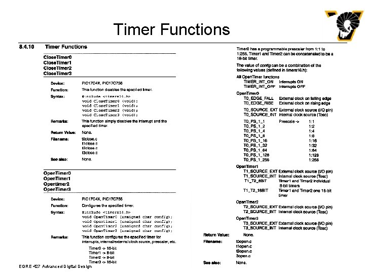
Timer Functions EGRE 427 Advanced Digital Design

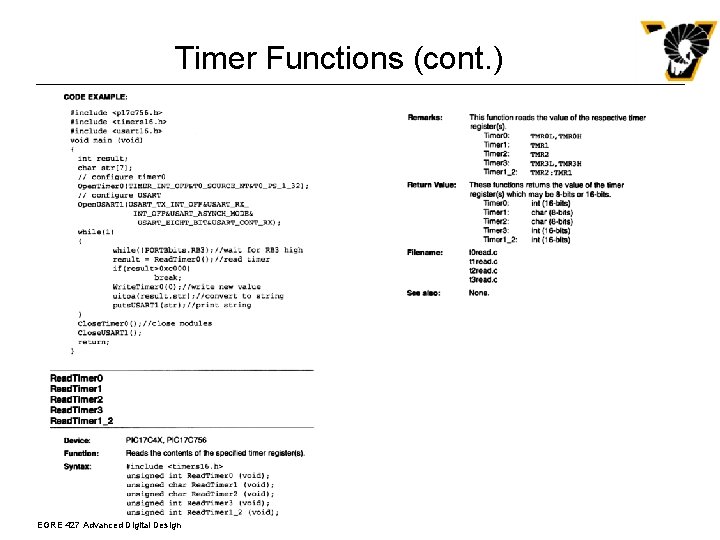
Timer Functions (cont. ) EGRE 427 Advanced Digital Design

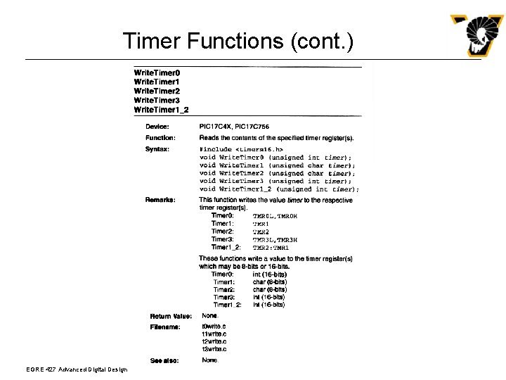
Timer Functions (cont. ) EGRE 427 Advanced Digital Design

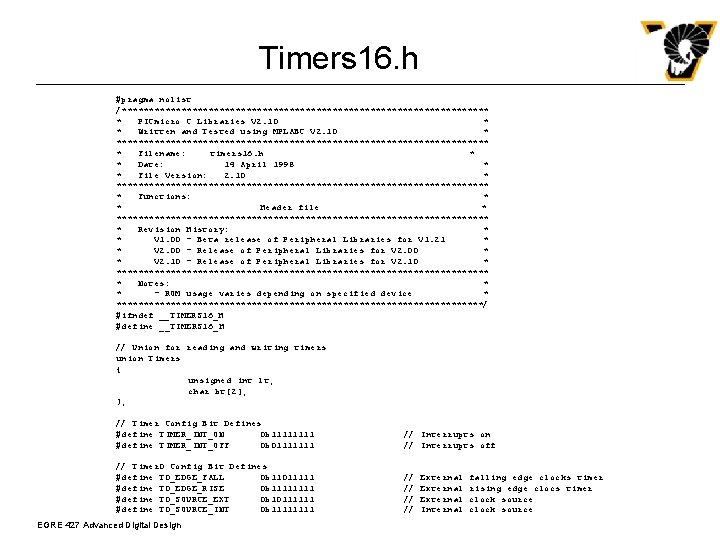
Timers 16. h #pragma nolist /********************************** * PICmicro C Libraries V 2. 10 * * Written and Tested using MPLABC V 2. 10 * *********************************** * Filename: timers 16. h * * Date: 14 April 1998 * * File Version: 2. 10 * *********************************** * Functions: * * Header file * *********************************** * Revision History: * * V 1. 00 - Beta release of Peripheral Libraries for V 1. 21 * * V 2. 00 - Release of Peripheral Libraries for V 2. 00 * * V 2. 10 - Release of Peripheral Libraries for V 2. 10 * *********************************** * Notes: * * - ROM usage varies depending on specified device * **********************************/ #ifndef __TIMERS 16_H #define __TIMERS 16_H // Union for reading and writing timers union Timers { unsigned int lt; char bt[2]; }; // Timer Config Bit Defines #define TIMER_INT_ON 0 b 1111 #define TIMER_INT_OFF 0 b 01111111 // Interrupts on // Interrupts off // Timer 0 Config Bit Defines #define T 0_EDGE_FALL 0 b 11011111 #define T 0_EDGE_RISE 0 b 1111 #define T 0_SOURCE_EXT 0 b 10111111 #define T 0_SOURCE_INT 0 b 1111 // // EGRE 427 Advanced Digital Design External Internal falling edge clocks timer rising edge clocs timer clock source

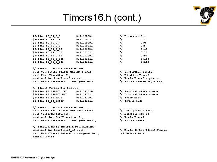
Timers 16. h (cont. ) #define #define #define T 0_PS_1_1 T 0_PS_1_2 T 0_PS_1_4 T 0_PS_1_8 T 0_PS_1_16 T 0_PS_1_32 T 0_PS_1_64 T 0_PS_1_128 T 0_PS_1_256 0 b 11100001 0 b 11100011 0 b 11100101 0 b 11100111 0 b 11101001 0 b 11101011 0 b 11101101 0 b 11101111 0 b 1111 // Prescaler 1: 1 // 1: 2 // 1: 4 // 1: 8 // 1: 16 // 1: 32 // 1: 64 // 1: 128 // 1: 256 // Timer 0 Function Declarations void Open. Timer 0(static unsigned char); void Close. Timer 0(void); unsigned int Read. Timer 0(void); void Write. Timer 0(static unsigned int); // // Configures Timer 0 Disables Timer 0 Reads Timer 0 registers Writes Timer 0 registers // Timer 1 Config Bit Defines #define T 1_SOURCE_INT 0 b 11111110 #define T 1_SOURCE_EXT 0 b 1111 #define T 1_T 2_8 BIT 0 b 11111101 #define T 1_T 2_16 BIT 0 b 1111 // // Internal clock source External clock source 8 -bit mode 16 -bit mode // Timer 1 Function Declarations void Open. Timer 1(static unsigned char); void Close. Timer 1(void); unsigned char Read. Timer 1(void); void Write. Timer 1(static unsigned char); // // Configures Timer 1 Disables Timer 1 Reads Timer 1 Writes Timer 1 // Timer 1: Timer 2 Function Declarations unsigned int Read. Timer 1_16(void); void Write. Timer 1_16(static unsigned int); Timer 2: Timer 1 EGRE 427 Advanced Digital Design // Reads 16 -bit Timer 2: Timer 1 // Writes 16 -bit

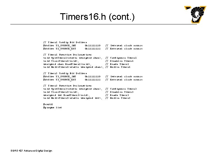
Timers 16. h (cont. ) // Timer 2 Config Bit Defines #define T 2_SOURCE_INT 0 b 11111110 #define T 2_SOURCE_EXT 0 b 1111 // Internal clock source // External clock source // Timer 2 Function Declarations void Open. Timer 2(static unsigned char); void Close. Timer 2(void); unsigned char Read. Timer 2(void); void Write. Timer 2(static unsigned char); // // // Timer 3 Config Bit Defines #define T 3_SOURCE_INT 0 b 11111110 #define T 3_SOURCE_EXT 0 b 1111 // Internal clock source // External clock source // Timer 3 Function Declarations void Open. Timer 3(static unsigned char); void Close. Timer 3(void); unsigned int Read. Timer 3(void); void Write. Timer 3(static unsigned int); // // #endif #pragma list EGRE 427 Advanced Digital Design Configures Timer 2 Disables Timer 2 Reads Timer 2 Writes Timer 2 Configures Timer 3 Disables Timer 3 Reads Timer 3 Writes Timer 3

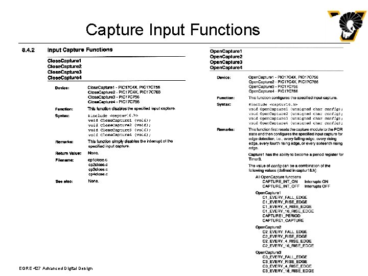
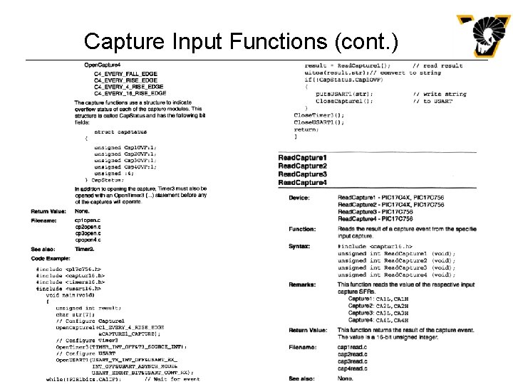
Capture Input Functions EGRE 427 Advanced Digital Design

Capture Input Functions (cont. ) EGRE 427 Advanced Digital Design

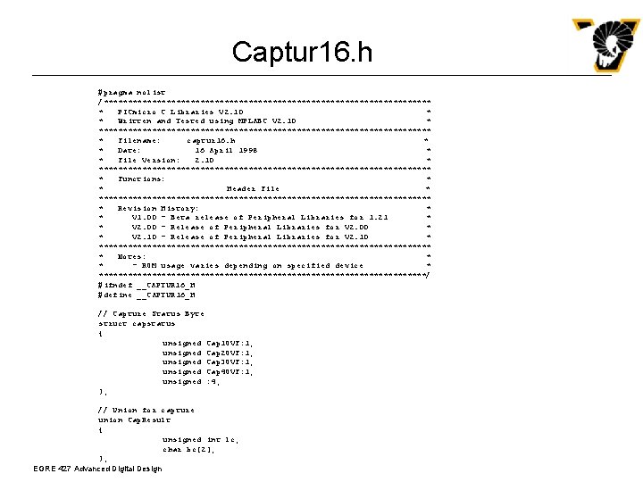
Captur 16. h #pragma nolist /********************************** * PICmicro C Libraries V 2. 10 * * Written and Tested using MPLABC V 2. 10 * *********************************** * Filename: captur 16. h * * Date: 16 April 1998 * * File Version: 2. 10 * *********************************** * Functions: * * Header File * *********************************** * Revision History: * * V 1. 00 - Beta release of Peripheral Libraries for 1. 21 * * V 2. 00 - Release of Peripheral Libraries for V 2. 00 * * V 2. 10 - Release of Peripheral Libraries for V 2. 10 * *********************************** * Notes: * * - ROM usage varies depending on specified device * **********************************/ #ifndef __CAPTUR 16_H #define __CAPTUR 16_H // Capture Status Byte struct capstatus { unsigned Cap 1 OVF: 1; unsigned Cap 2 OVF: 1; unsigned Cap 3 OVF: 1; unsigned Cap 4 OVF: 1; unsigned : 4; }; // Union for capture union Cap. Result { unsigned int lc; char bc[2]; }; EGRE 427 Advanced Digital Design

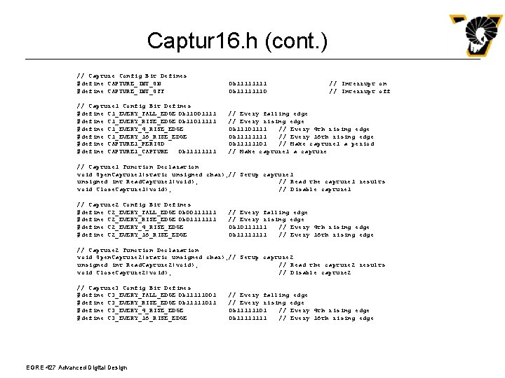
Captur 16. h (cont. ) // Capture Config Bit Defines #define CAPTURE_INT_ON #define CAPTURE_INT_OFF 0 b 11111110 // Capture 1 Config Bit Defines #define C 1_EVERY_FALL_EDGE 0 b 11001111 #define C 1_EVERY_RISE_EDGE 0 b 11011111 #define C 1_EVERY_4_RISE_EDGE #define C 1_EVERY_16_RISE_EDGE #define CAPTURE 1_PERIOD #define CAPTURE 1_CAPTURE 0 b 1111 // Every falling edge // Every rising edge 0 b 11101111 // Every 4 th rising edge 0 b 1111 // Every 16 th rising edge 0 b 11111101 // Make capture 1 a period // Make capture 1 a capture // Interrupt on // Interrupt off // Capture 1 Function Declaration void Open. Capture 1(static unsigned char); // Setup capture 1 unsigned int Read. Capture 1(void); // Read the capture 1 results void Close. Capture 1(void); // Disable capture 1 // Capture 2 Config Bit Defines #define C 2_EVERY_FALL_EDGE 0 b 00111111 #define C 2_EVERY_RISE_EDGE 0 b 01111111 #define C 2_EVERY_4_RISE_EDGE #define C 2_EVERY_16_RISE_EDGE // Every falling edge // Every rising edge 0 b 10111111 // Every 4 th rising edge 0 b 1111 // Every 16 th rising edge // Capture 2 Function Declaration void Open. Capture 2(static unsigned char); // Setup capture 2 unsigned int Read. Capture 2(void); // Read the capture 2 results void Close. Capture 2(void); // Disable capture 2 // Capture 3 Config Bit Defines #define C 3_EVERY_FALL_EDGE 0 b 11111001 #define C 3_EVERY_RISE_EDGE 0 b 11111011 #define C 3_EVERY_4_RISE_EDGE #define C 3_EVERY_16_RISE_EDGE EGRE 427 Advanced Digital Design // Every falling edge // Every rising edge 0 b 11111101 // Every 4 th rising edge 0 b 1111 // Every 16 th rising edge

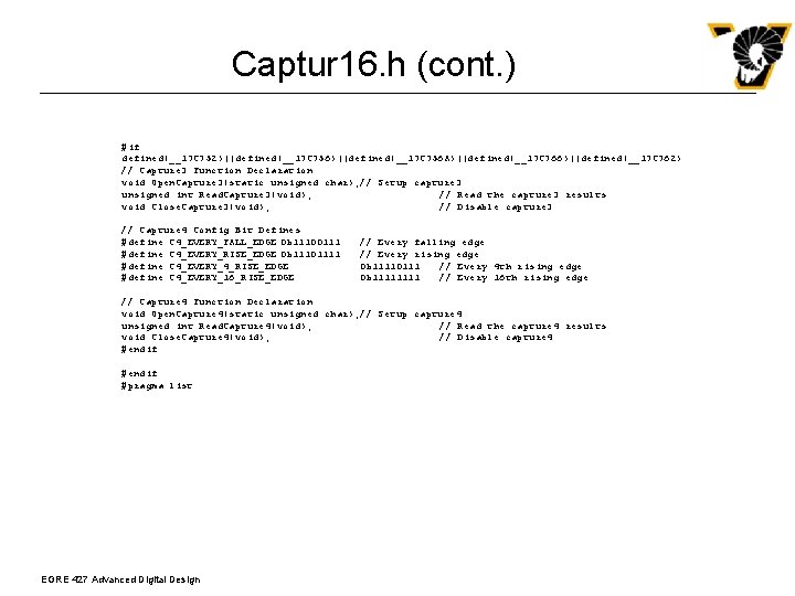
Captur 16. h (cont. ) #if defined(__17 C 752)||defined(__17 C 756 A)||defined(__17 C 766)||defined(__17 C 762) // Capture 3 Function Declaration void Open. Capture 3(static unsigned char); // Setup capture 3 unsigned int Read. Capture 3(void); // Read the capture 3 results void Close. Capture 3(void); // Disable capture 3 // Capture 4 Config Bit Defines #define C 4_EVERY_FALL_EDGE 0 b 11100111 #define C 4_EVERY_RISE_EDGE 0 b 11101111 #define C 4_EVERY_4_RISE_EDGE #define C 4_EVERY_16_RISE_EDGE // Every falling edge // Every rising edge 0 b 11110111 // Every 4 th rising edge 0 b 1111 // Every 16 th rising edge // Capture 4 Function Declaration void Open. Capture 4(static unsigned char); // Setup capture 4 unsigned int Read. Capture 4(void); // Read the capture 4 results void Close. Capture 4(void); // Disable capture 4 #endif #pragma list EGRE 427 Advanced Digital Design

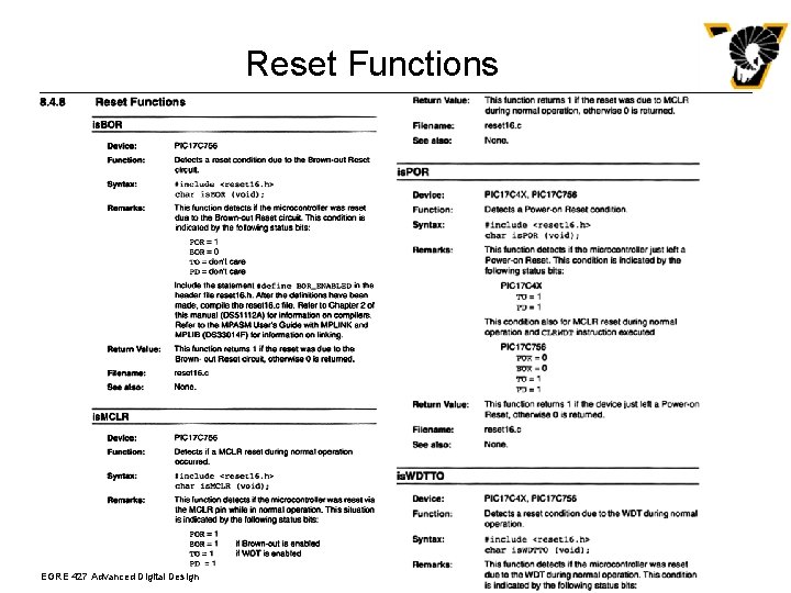
Reset Functions EGRE 427 Advanced Digital Design

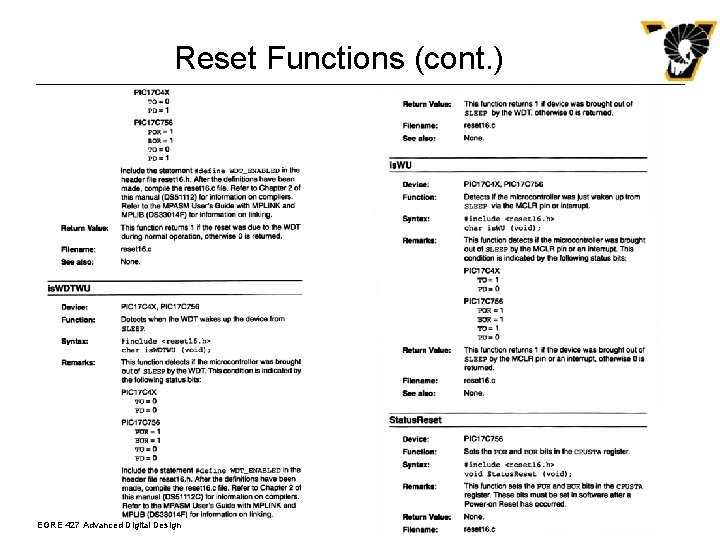
Reset Functions (cont. ) EGRE 427 Advanced Digital Design

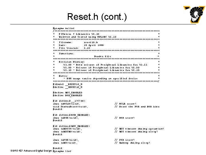
Reset. h (cont. ) #pragma nolist /********************************** * PICmicro C Libraries V 2. 10 * * Written and Tested using MPLABC V 2. 10 * *********************************** * Filename: reset 16. h * * Date: 14 April 1998 * * File Version: 2. 10 * *********************************** * Functions: * * Header file * *********************************** * Revision History: * * V 1. 00 - Beta release of Peripheral Libraries for V 1. 21 * * V 2. 00 - Release of Peripheral Libraries for V 2. 00 * * V 2. 10 - Release of Peripheral Libraries for V 2. 10 * *********************************** * Notes: * * - ROM usage varies depending on specified device * **********************************/ #ifndef __RESET 16_H #define WDT_ENABLED #define BOR_ENABLED #if defined(__17 C 756) char is. MCLR(void); void Status. Reset(void); #endif // MCLR reset? // Reset the POR and BOR bits #if defined(BOR_ENABLED) char is. BOR(void); #endif // BOR reset? #if defined(WDT_ENABLED) char is. WDTTO(void); char is. WDTWU(void); #endif // WDT timeout during operation? // WDT timeout during sleep? char is. POR(void); char is. WU(void); // POR reset? // Wakeup during sleep? #endif EGRE 427 Advanced Digital Design #pragma list

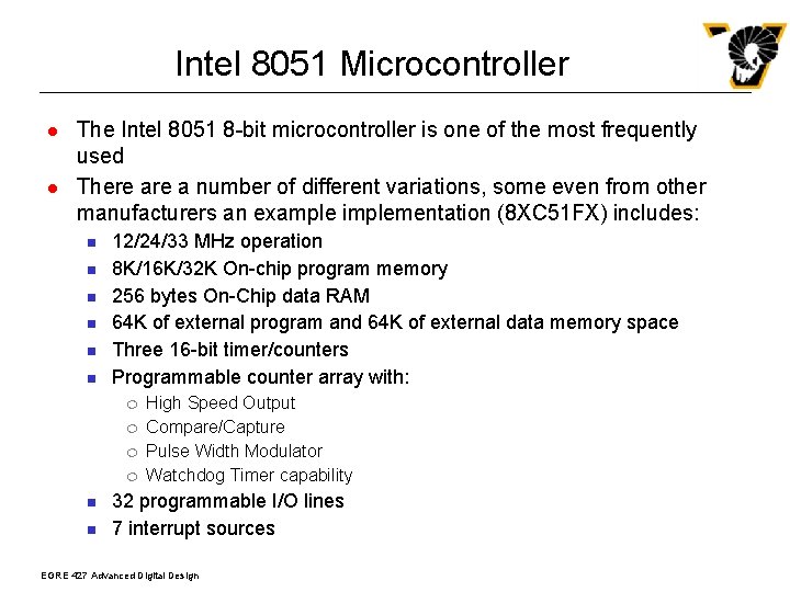
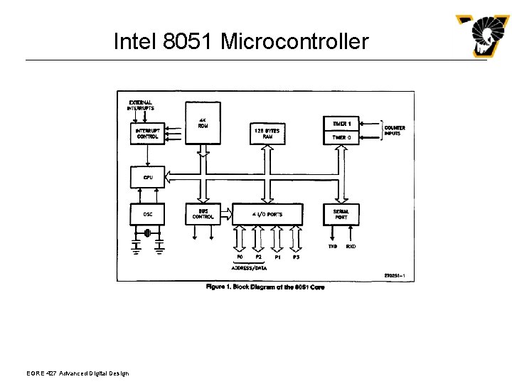
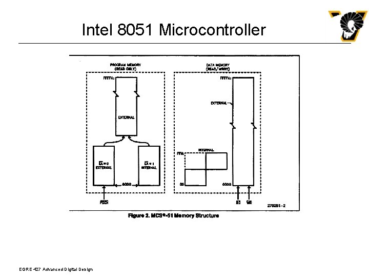
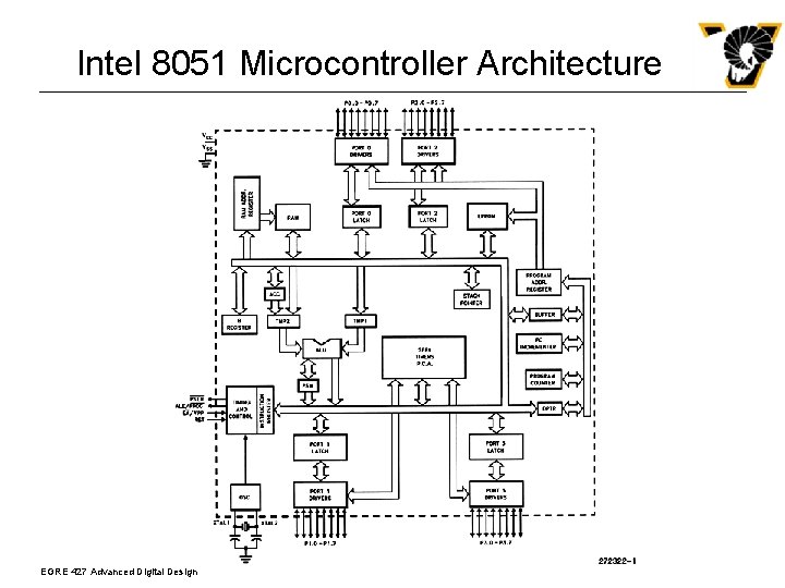
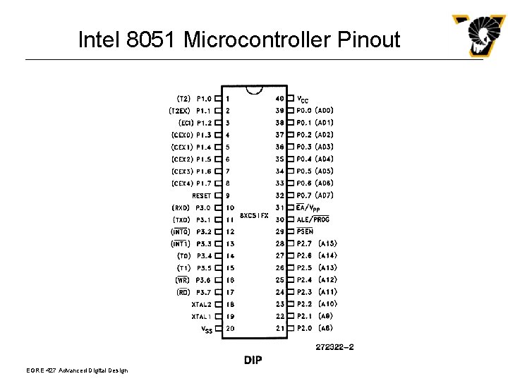
Intel 8051 Microcontroller l l The Intel 8051 8 -bit microcontroller is one of the most frequently used There a number of different variations, some even from other manufacturers an example implementation (8 XC 51 FX) includes: n n n 12/24/33 MHz operation 8 K/16 K/32 K On-chip program memory 256 bytes On-Chip data RAM 64 K of external program and 64 K of external data memory space Three 16 -bit timer/counters Programmable counter array with: ¦ ¦ n n High Speed Output Compare/Capture Pulse Width Modulator Watchdog Timer capability 32 programmable I/O lines 7 interrupt sources EGRE 427 Advanced Digital Design

Intel 8051 Microcontroller EGRE 427 Advanced Digital Design

Intel 8051 Microcontroller EGRE 427 Advanced Digital Design

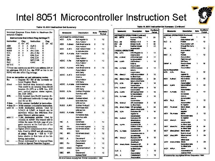
Intel 8051 Microcontroller Instruction Set EGRE 427 Advanced Digital Design

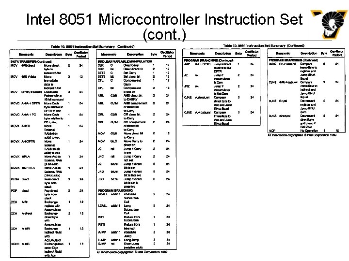
Intel 8051 Microcontroller Instruction Set (cont. ) EGRE 427 Advanced Digital Design

Intel 8051 Microcontroller Architecture EGRE 427 Advanced Digital Design

Intel 8051 Microcontroller Pinout EGRE 427 Advanced Digital Design

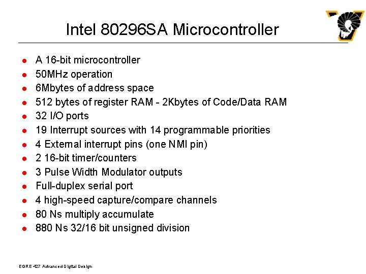
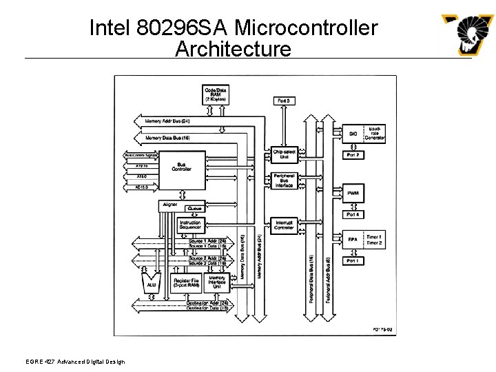
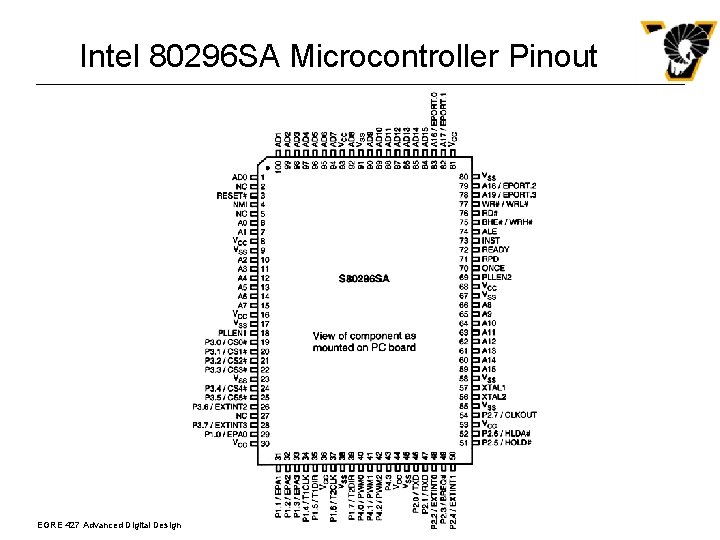
Intel 80296 SA Microcontroller l l l l A 16 -bit microcontroller 50 MHz operation 6 Mbytes of address space 512 bytes of register RAM - 2 Kbytes of Code/Data RAM 32 I/O ports 19 Interrupt sources with 14 programmable priorities 4 External interrupt pins (one NMI pin) 2 16 -bit timer/counters 3 Pulse Width Modulator outputs Full-duplex serial port 4 high-speed capture/compare channels 80 Ns multiply accumulate 880 Ns 32/16 bit unsigned division EGRE 427 Advanced Digital Design

Intel 80296 SA Microcontroller Architecture EGRE 427 Advanced Digital Design

Intel 80296 SA Microcontroller Pinout EGRE 427 Advanced Digital Design

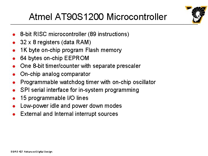
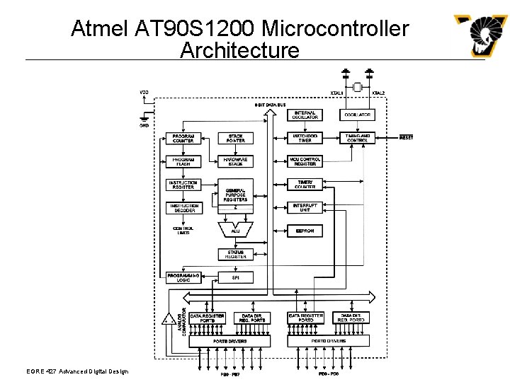
Atmel AT 90 S 1200 Microcontroller l l l 8 -bit RISC microcontroller (89 instructions) 32 x 8 registers (data RAM) 1 K byte on-chip program Flash memory 64 bytes on-chip EEPROM One 8 -bit timer/counter with separate prescaler On-chip analog comparator Programmable watchdog timer with on-chip oscillator SPI serial interface for in-system programming 15 programmable I/O lines Low-power idle and power down modes External and Internal interrupt sources EGRE 427 Advanced Digital Design

Atmel AT 90 S 1200 Microcontroller Architecture EGRE 427 Advanced Digital Design

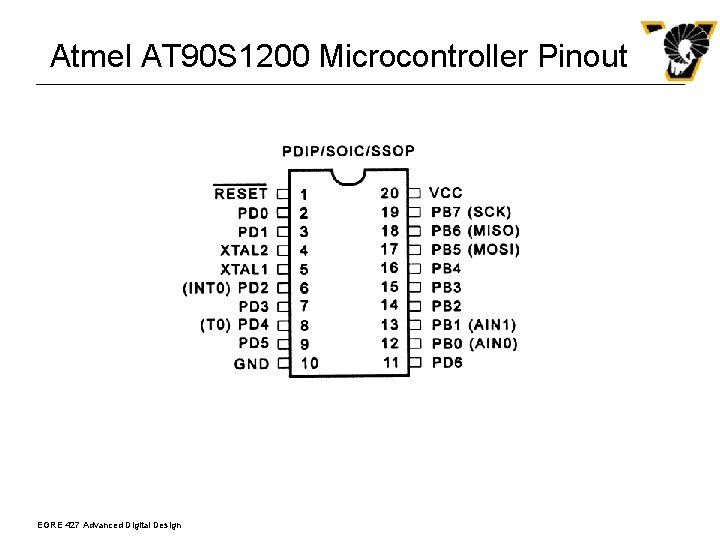
Atmel AT 90 S 1200 Microcontroller Pinout EGRE 427 Advanced Digital Design

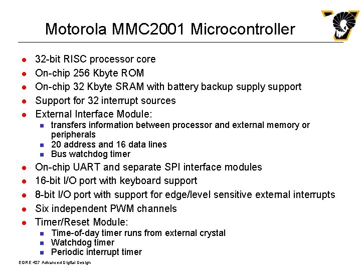
Motorola MMC 2001 Microcontroller l l l 32 -bit RISC processor core On-chip 256 Kbyte ROM On-chip 32 Kbyte SRAM with battery backup supply support Support for 32 interrupt sources External Interface Module: n n n l l l transfers information between processor and external memory or peripherals 20 address and 16 data lines Bus watchdog timer On-chip UART and separate SPI interface modules 16 -bit I/O port with keyboard support 8 -bit I/O port with support for edge/level sensitive external interrupts Six independent PWM channels Timer/Reset Module: n n n Time-of-day timer runs from external crystal Watchdog timer Periodic interrupt timer EGRE 427 Advanced Digital Design

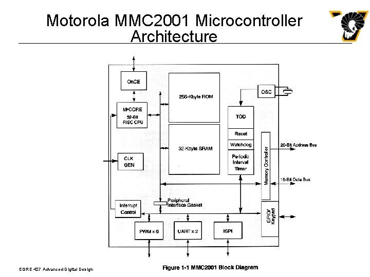
Motorola MMC 2001 Microcontroller Architecture EGRE 427 Advanced Digital Design

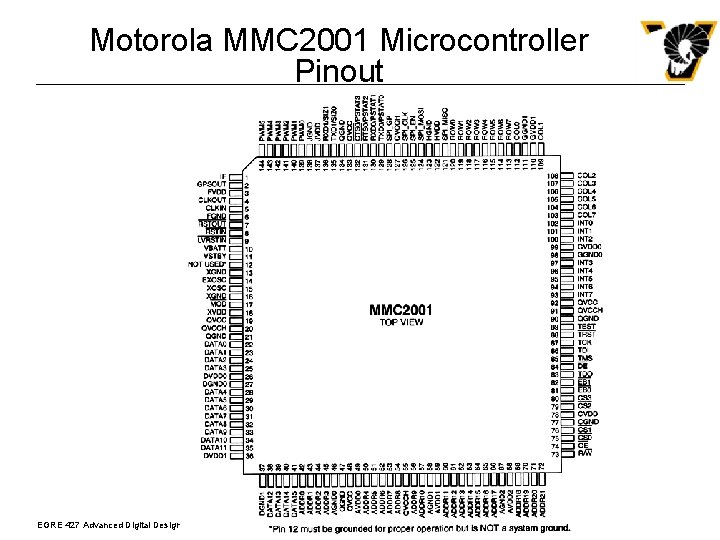
Motorola MMC 2001 Microcontroller Pinout EGRE 427 Advanced Digital Design