Chapter 2 CMOS Logic ApplicationSpecific Integrated Circuits Michael
- Slides: 35

Chapter 2 CMOS Logic Application-Specific Integrated Circuits Michael John Sebastian Smith Addison Wesley, 1997 EGRE 427 Advanced Digital Design Figures from Application-Specific Integrated Circuits , Michael John Sebastian Smith, Addison Wesley, 1997

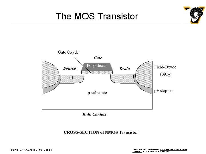
The MOS Transistor EGRE 427 Advanced Digital Design Figures from material provided with Digital. Circuits Integrated Circuits, A Design Figures from Application-Specific Integrated , Michael John Sebastian Perspective, Jan Rabaey, Smith, Addison by Wesley, 1997 Prentice Hall, 1996

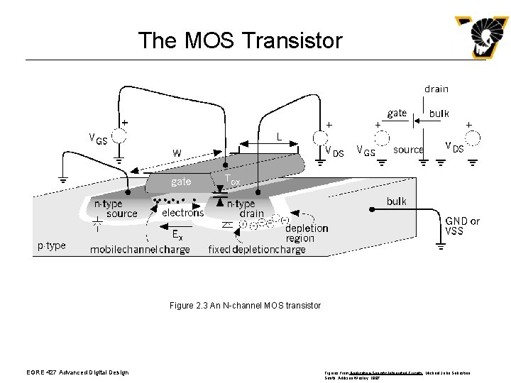
The MOS Transistor Figure 2. 3 An N-channel MOS transistor EGRE 427 Advanced Digital Design Figures from Application-Specific Integrated Circuits , Michael John Sebastian Smith, Addison Wesley, 1997

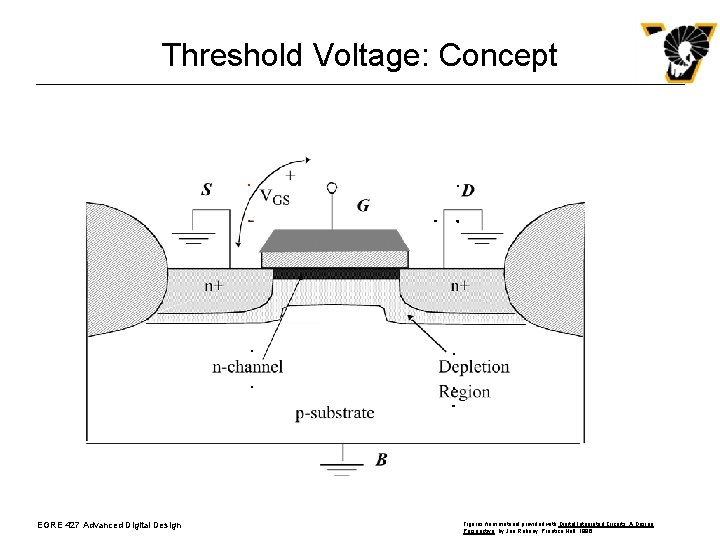
Threshold Voltage: Concept EGRE 427 Advanced Digital Design Figures from material provided with Digital. Circuits Integrated Circuits, A Design Figures from Application-Specific Integrated , Michael John Sebastian Perspective, Jan Rabaey, Smith, Addison by Wesley, 1997 Prentice Hall, 1996

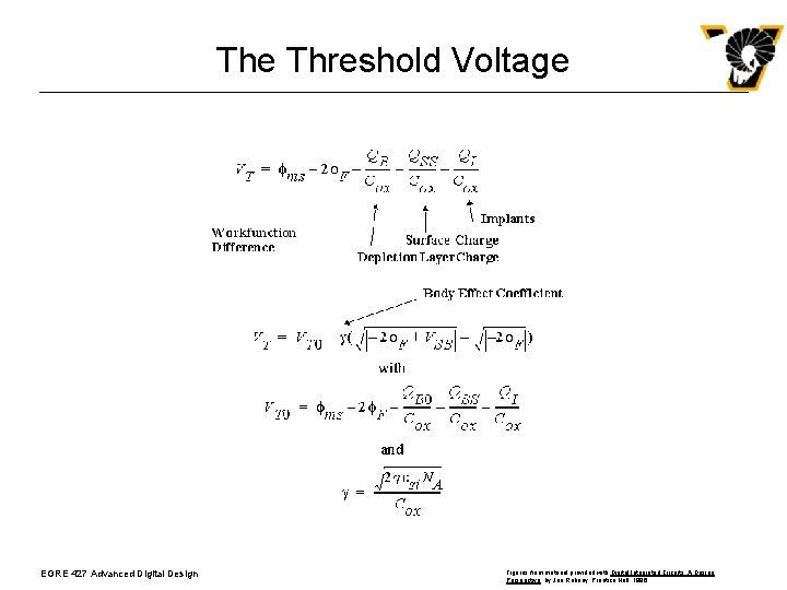
The Threshold Voltage EGRE 427 Advanced Digital Design Figures from material provided with Digital. Circuits Integrated Circuits, A Design Figures from Application-Specific Integrated , Michael John Sebastian Perspective, Jan Rabaey, Smith, Addison by Wesley, 1997 Prentice Hall, 1996

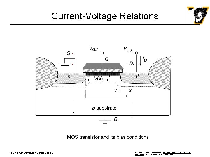
Current-Voltage Relations EGRE 427 Advanced Digital Design Figures from material provided with Digital. Circuits Integrated Circuits, A Design Figures from Application-Specific Integrated , Michael John Sebastian Perspective, Jan Rabaey, Smith, Addison by Wesley, 1997 Prentice Hall, 1996

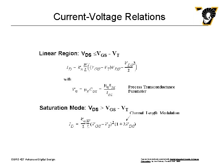
Current-Voltage Relations EGRE 427 Advanced Digital Design Figures from material provided with Digital. Circuits Integrated Circuits, A Design Figures from Application-Specific Integrated , Michael John Sebastian Perspective, Jan Rabaey, Smith, Addison by Wesley, 1997 Prentice Hall, 1996

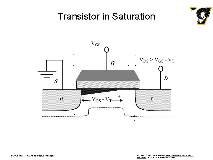
Transistor in Saturation EGRE 427 Advanced Digital Design Figures from material provided with Digital. Circuits Integrated Circuits, A Design Figures from Application-Specific Integrated , Michael John Sebastian Perspective, Jan Rabaey, Smith, Addison by Wesley, 1997 Prentice Hall, 1996

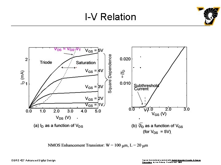
I-V Relation EGRE 427 Advanced Digital Design Figures from material provided with Digital. Circuits Integrated Circuits, A Design Figures from Application-Specific Integrated , Michael John Sebastian Perspective, Jan Rabaey, Smith, Addison by Wesley, 1997 Prentice Hall, 1996

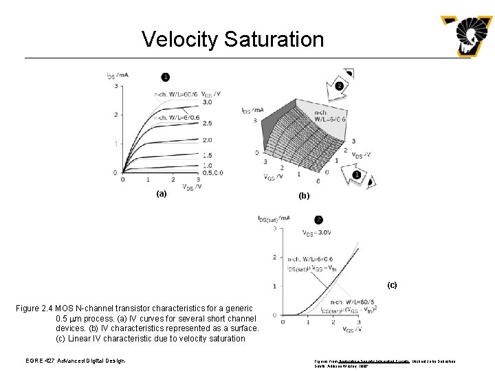
Velocity Saturation (a) (b) (c) Figure 2. 4 MOS N-channel transistor characteristics for a generic 0. 5 mm process. (a) IV curves for several short channel devices. (b) IV characteristics represented as a surface. (c) Linear IV characteristic due to velocity saturation EGRE 427 Advanced Digital Design Figures from Application-Specific Integrated Circuits , Michael John Sebastian Smith, Addison Wesley, 1997

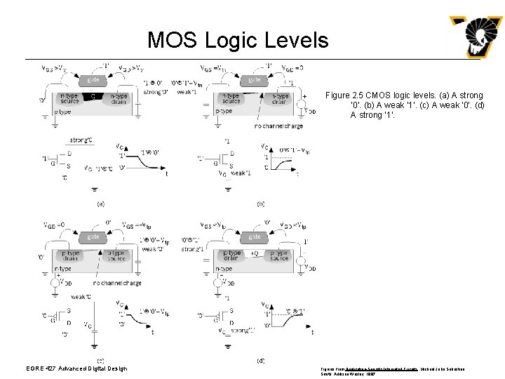
MOS Logic Levels Figure 2. 5 CMOS logic levels. (a) A strong ‘ 0’. (b) A weak ‘ 1’. (c) A weak ‘ 0’. (d) A strong ‘ 1’. EGRE 427 Advanced Digital Design Figures from Application-Specific Integrated Circuits , Michael John Sebastian Smith, Addison Wesley, 1997

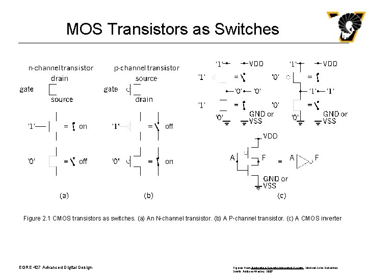
MOS Transistors as Switches Figure 2. 1 CMOS transistors as switches. (a) An N-channel transistor. (b) A P-channel transistor. (c) A CMOS inverter EGRE 427 Advanced Digital Design Figures from Application-Specific Integrated Circuits , Michael John Sebastian Smith, Addison Wesley, 1997

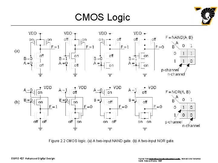
CMOS Logic Figure 2. 2 CMOS logic. (a) A two-input NAND gate. (b) A two-input NOR gate. EGRE 427 Advanced Digital Design Figures from Application-Specific Integrated Circuits , Michael John Sebastian Smith, Addison Wesley, 1997

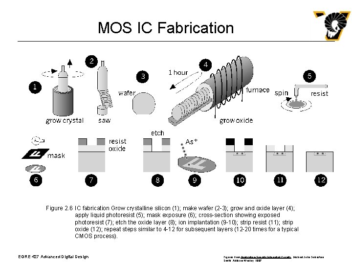
MOS IC Fabrication Figure 2. 6 IC fabrication Grow crystalline silicon (1); make wafer (2 -3); grow and oxide layer (4); apply liquid photoresist (5); mask exposure (6); cross-section showing exposed photoresist (7); etch the oxide layer (8); ion implantation (9 -10); strip resist (11); strip oxide (12); repeat steps similar to 4 -12 for subsequent layers (12 -20 times for a typical CMOS process). EGRE 427 Advanced Digital Design Figures from Application-Specific Integrated Circuits , Michael John Sebastian Smith, Addison Wesley, 1997

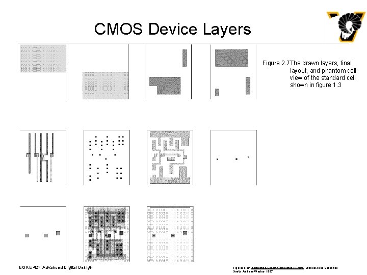
CMOS Device Layers Figure 2. 7 The drawn layers, final layout, and phantom cell view of the standard cell shown in figure 1. 3 EGRE 427 Advanced Digital Design Figures from Application-Specific Integrated Circuits , Michael John Sebastian Smith, Addison Wesley, 1997

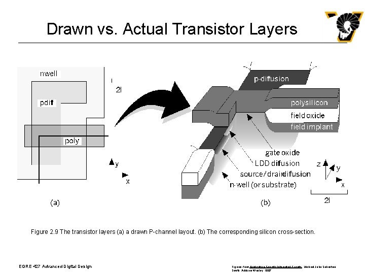
Drawn vs. Actual Transistor Layers Figure 2. 9 The transistor layers (a) a drawn P-channel layout. (b) The corresponding silicon cross-section. EGRE 427 Advanced Digital Design Figures from Application-Specific Integrated Circuits , Michael John Sebastian Smith, Addison Wesley, 1997

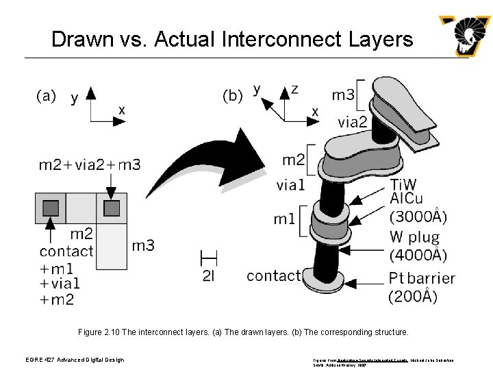
Drawn vs. Actual Interconnect Layers Figure 2. 10 The interconnect layers. (a) The drawn layers. (b) The corresponding structure. EGRE 427 Advanced Digital Design Figures from Application-Specific Integrated Circuits , Michael John Sebastian Smith, Addison Wesley, 1997

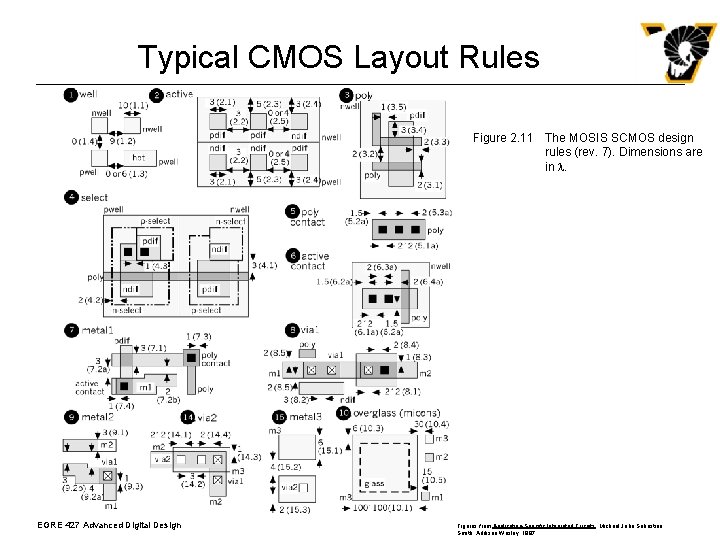
Typical CMOS Layout Rules Figure 2. 11 The MOSIS SCMOS design rules (rev. 7). Dimensions are in l. EGRE 427 Advanced Digital Design Figures from Application-Specific Integrated Circuits , Michael John Sebastian Smith, Addison Wesley, 1997

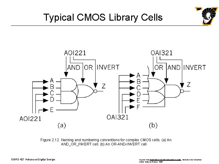
Typical CMOS Library Cells Figure 2. 12 Naming and numbering conventions for complex CMOS cells. (a) An AND_OR_INVERT cell. (b) An OR-AND-INVERT cell EGRE 427 Advanced Digital Design Figures from Application-Specific Integrated Circuits , Michael John Sebastian Smith, Addison Wesley, 1997

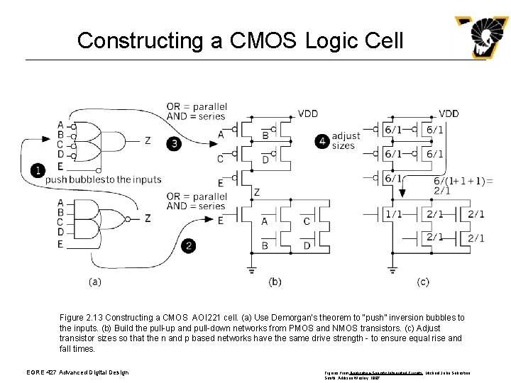
Constructing a CMOS Logic Cell Figure 2. 13 Constructing a CMOS AOI 221 cell. (a) Use Demorgan’s theorem to “push” inversion bubbles to the inputs. (b) Build the pull-up and pull-down networks from PMOS and NMOS transistors. (c) Adjust transistor sizes so that the n and p based networks have the same drive strength - to ensure equal rise and fall times. EGRE 427 Advanced Digital Design Figures from Application-Specific Integrated Circuits , Michael John Sebastian Smith, Addison Wesley, 1997

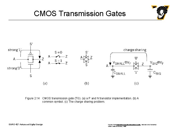
CMOS Transmission Gates Figure 2. 14 CMOS transmission gate (TG). (a) a P and N transistor implementation. (b) A common symbol. (c) The charge sharing problem. EGRE 427 Advanced Digital Design Figures from Application-Specific Integrated Circuits , Michael John Sebastian Smith, Addison Wesley, 1997

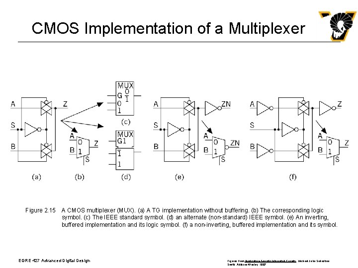
CMOS Implementation of a Multiplexer Figure 2. 15 A CMOS multiplexer (MUX). (a) A TG implementation without buffering. (b) The corresponding logic symbol. (c) The IEEE standard symbol. (d) an alternate (non-standard) IEEE symbol. (e) An inverting, buffered implementation and its logic symbol. (f) a non-inverting, buffered implementation and its symbol. EGRE 427 Advanced Digital Design Figures from Application-Specific Integrated Circuits , Michael John Sebastian Smith, Addison Wesley, 1997

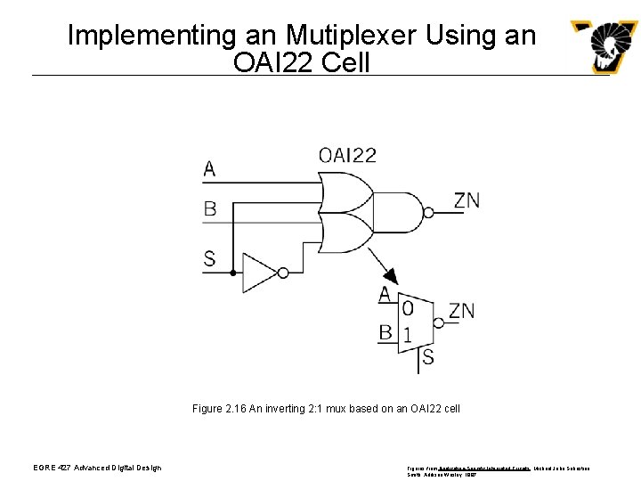
Implementing an Mutiplexer Using an OAI 22 Cell Figure 2. 16 An inverting 2: 1 mux based on an OAI 22 cell EGRE 427 Advanced Digital Design Figures from Application-Specific Integrated Circuits , Michael John Sebastian Smith, Addison Wesley, 1997

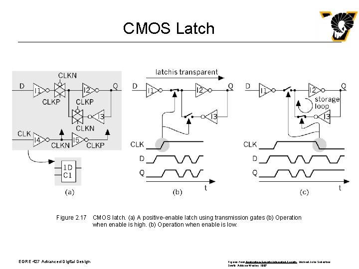
CMOS Latch Figure 2. 17 CMOS latch. (a) A positive-enable latch using transmission gates (b) Operation when enable is high. (b) Operation when enable is low. EGRE 427 Advanced Digital Design Figures from Application-Specific Integrated Circuits , Michael John Sebastian Smith, Addison Wesley, 1997

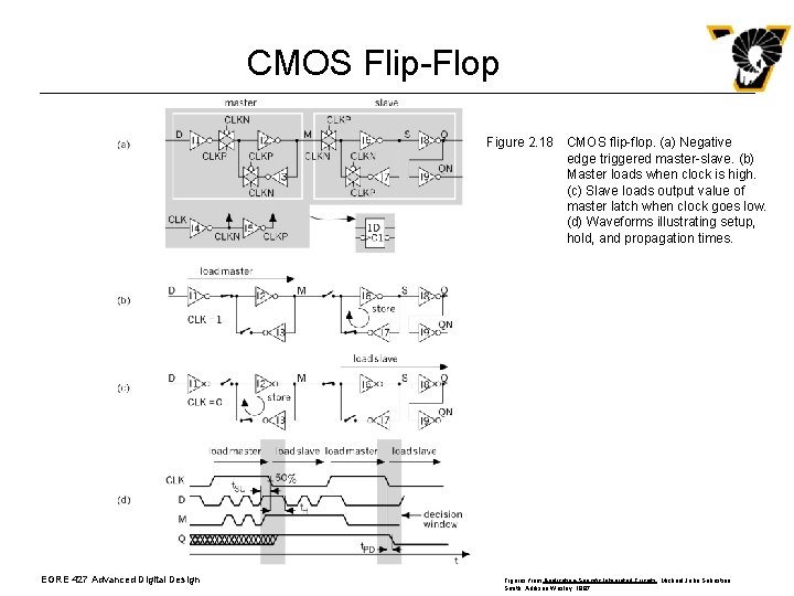
CMOS Flip-Flop Figure 2. 18 CMOS flip-flop. (a) Negative edge triggered master-slave. (b) Master loads when clock is high. (c) Slave loads output value of master latch when clock goes low. (d) Waveforms illustrating setup, hold, and propagation times. EGRE 427 Advanced Digital Design Figures from Application-Specific Integrated Circuits , Michael John Sebastian Smith, Addison Wesley, 1997

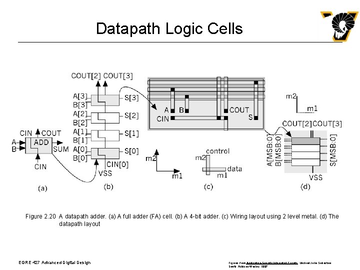
Datapath Logic Cells Figure 2. 20 A datapath adder. (a) A full adder (FA) cell. (b) A 4 -bit adder. (c) Wiring layout using 2 level metal. (d) The datapath layout EGRE 427 Advanced Digital Design Figures from Application-Specific Integrated Circuits , Michael John Sebastian Smith, Addison Wesley, 1997

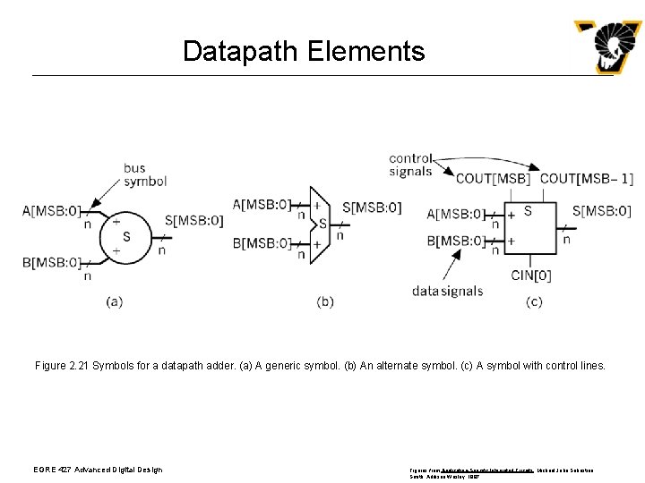
Datapath Elements Figure 2. 21 Symbols for a datapath adder. (a) A generic symbol. (b) An alternate symbol. (c) A symbol with control lines. EGRE 427 Advanced Digital Design Figures from Application-Specific Integrated Circuits , Michael John Sebastian Smith, Addison Wesley, 1997

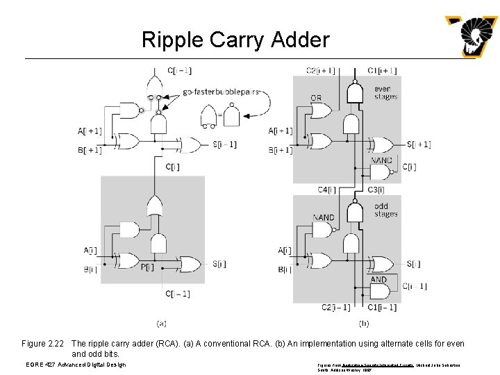
Ripple Carry Adder Figure 2. 22 The ripple carry adder (RCA). (a) A conventional RCA. (b) An implementation using alternate cells for even and odd bits. EGRE 427 Advanced Digital Design Figures from Application-Specific Integrated Circuits , Michael John Sebastian Smith, Addison Wesley, 1997

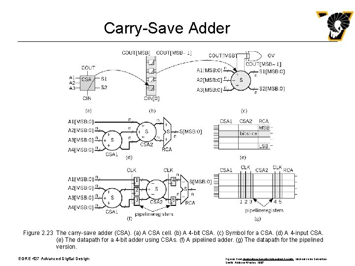
Carry-Save Adder Figure 2. 23 The carry-save adder (CSA). (a) A CSA cell. (b) A 4 -bit CSA. (c) Symbol for a CSA. (d) A 4 -input CSA. (e) The datapath for a 4 -bit adder using CSAs. (f) A pipelined adder. (g) The datapath for the pipelined version. EGRE 427 Advanced Digital Design Figures from Application-Specific Integrated Circuits , Michael John Sebastian Smith, Addison Wesley, 1997

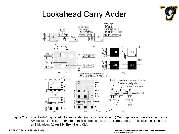
Lookahead Carry Adder Figure 2. 24 The Brent-Kung carry-lookahead adder. (a) Carry generation. (b) Cell to generate look-ahead terms. (c) Arrangement of cells. (d) and (e) Simplified representations of parts a and c. (f) The lookahead logic for an 8 bit adder. (g) An 8 bit Brent-Kung CLA. EGRE 427 Advanced Digital Design Figures from Application-Specific Integrated Circuits , Michael John Sebastian Smith, Addison Wesley, 1997

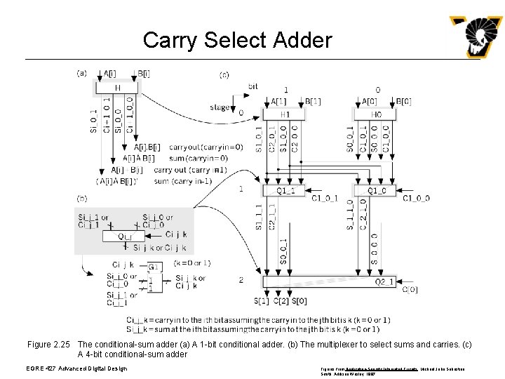
Carry Select Adder Figure 2. 25 The conditional-sum adder (a) A 1 -bit conditional adder. (b) The multiplexer to select sums and carries. (c) A 4 -bit conditional-sum adder EGRE 427 Advanced Digital Design Figures from Application-Specific Integrated Circuits , Michael John Sebastian Smith, Addison Wesley, 1997

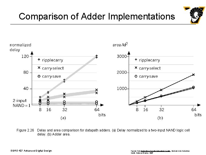
Comparison of Adder Implementations Figure 2. 26 Delay and area comparison for datapath adders. (a) Delay normalized to a two-input NAND logic cell delay. (b) Adder area. EGRE 427 Advanced Digital Design Figures from Application-Specific Integrated Circuits , Michael John Sebastian Smith, Addison Wesley, 1997

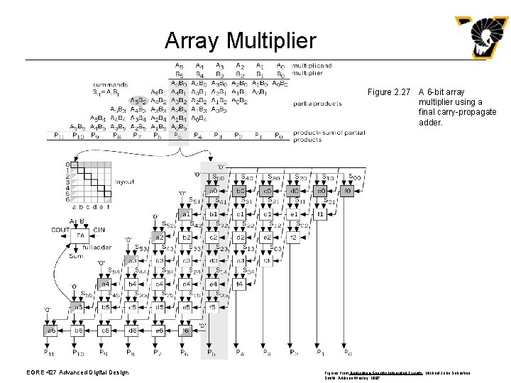
Array Multiplier Figure 2. 27 A 6 -bit array multiplier using a final carry-propagate adder. EGRE 427 Advanced Digital Design Figures from Application-Specific Integrated Circuits , Michael John Sebastian Smith, Addison Wesley, 1997

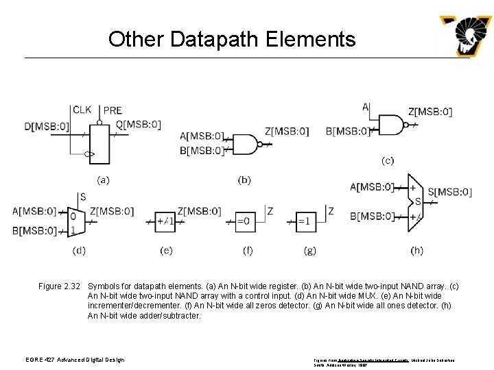
Other Datapath Elements Figure 2. 32 Symbols for datapath elements. (a) An N-bit wide register. (b) An N-bit wide two-input NAND array. (c) An N-bit wide two-input NAND array with a control input. (d) An N-bit wide MUX. (e) An N-bit wide incrementer/decrementer. (f) An N-bit wide all zeros detector. (g) An N-bit wide all ones detector. (h) An N-bit wide adder/subtracter. EGRE 427 Advanced Digital Design Figures from Application-Specific Integrated Circuits , Michael John Sebastian Smith, Addison Wesley, 1997

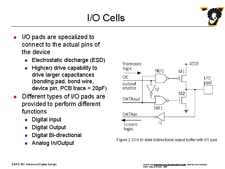
I/O Cells l I/O pads are specalized to connect to the actual pins of the device n n l Electrostatic discharge (ESD) High(er) drive capability to drive larger capacitances (bonding pad, bond wire, device pin, PCB trace > 20 p. F) Different types of I/O pads are provided to perform different functions n n Digital input Digital Output Digital Bi-directional Analog In/Output EGRE 427 Advanced Digital Design Figure 2. 33 A tri-state bidirectional output buffer with I/O pad. Figures from Application-Specific Integrated Circuits , Michael John Sebastian Smith, Addison Wesley, 1997