FarForward Calorimetry with the Si D and FCAL




- Slides: 41

Far-Forward Calorimetry with the Si. D and FCAL collaborations ALCW 15 Meeting, KEK April 20 -24 2015 Bruce Schumm UC Santa Cruz Institute for Particle Physics

FCAL Collaboration Si. D efforts on ILC far-forward calorimetry (Lumi. Cal, Beam. Cal are done within the context of the broad FCAL collaboration ~70 physicists; ~20 institutions Current Si. D contributions are solely to Beam. Cal: *) Front-end electronics design (BEAN chip) *) Sensor technology studies (SLAC T 506 radiation damage studies) *) Beamcal reconstruction and physics studies 2

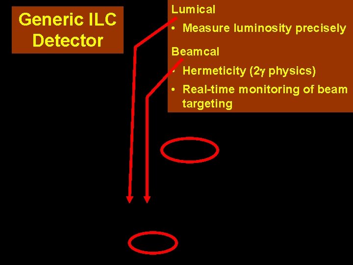
Generic ILC Detector Lumical • Measure luminosity precisely Beamcal • Hermeticity (2 physics) • Real-time monitoring of beam targeting 3

Beam. Cal Front-End Electronics (BEAN Chip) Lead: Prof. Angel Abusleme Pontifica Universidad Catolica de Chile 4

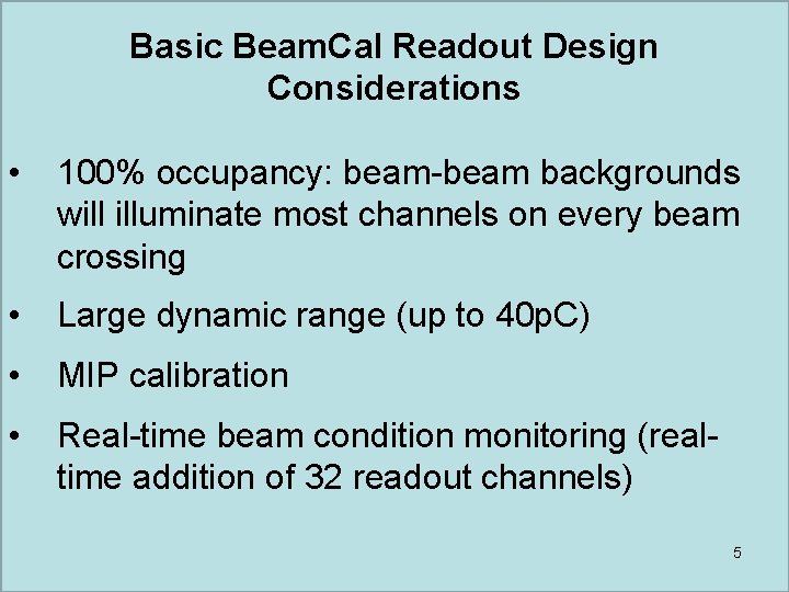
Basic Beam. Cal Readout Design Considerations • 100% occupancy: beam-beam backgrounds will illuminate most channels on every beam crossing • Large dynamic range (up to 40 p. C) • MIP calibration • Real-time beam condition monitoring (realtime addition of 32 readout channels) 5

6

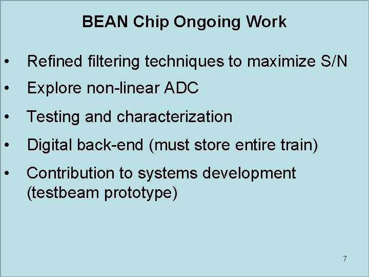
BEAN Chip Ongoing Work • Refined filtering techniques to maximize S/N • Explore non-linear ADC • Testing and characterization • Digital back-end (must store entire train) • Contribution to systems development (testbeam prototype) 7

SLAC T 506 Electromagentic Radiation Damage Study Update and Plans 8

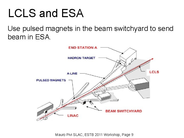
LCLS and ESA Use pulsed magnets in the beam switchyard to send beam in ESA. Mauro Pivi SLAC, ESTB 2011 Workshop, Page 9

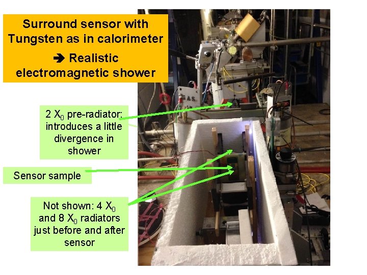
Surround sensor with Tungsten as in calorimeter Realistic electromagnetic shower 2 X 0 pre-radiator; introduces a little divergence in shower Sensor sample Not shown: 4 X 0 and 8 X 0 radiators just before and after sensor

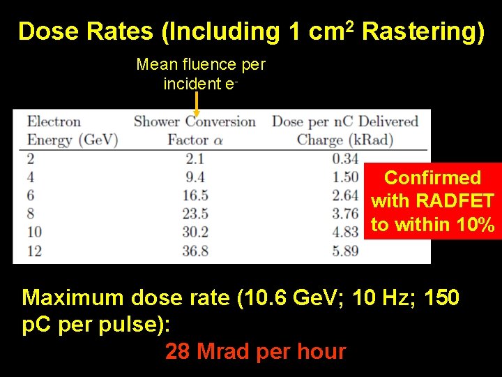
Dose Rates (Including 1 cm 2 Rastering) Mean fluence per incident e- Confirmed with RADFET to within 10% Maximum dose rate (10. 6 Ge. V; 10 Hz; 150 p. C per pulse): 11 28 Mrad per hour

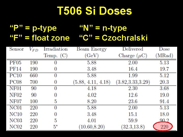
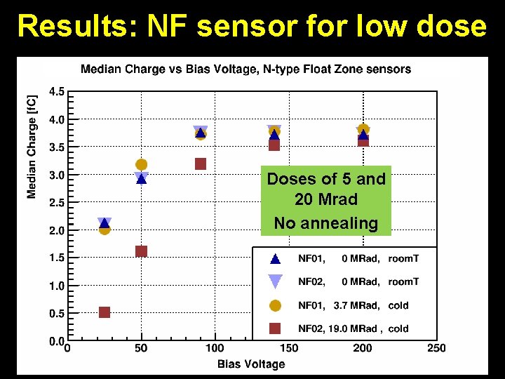
T 506 Si Doses “P” = p-type “F” = float zone “N” = n-type “C” = Czochralski 12

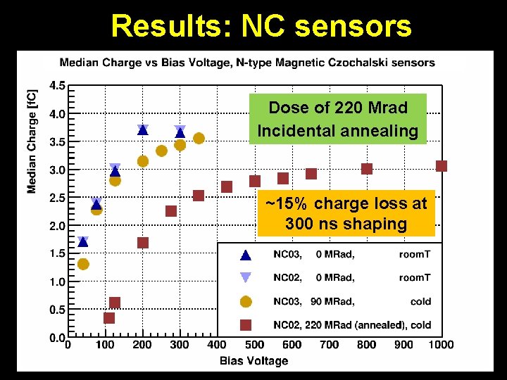
Results: NC sensors Dose of 220 Mrad Incidental annealing ~15% charge loss at 300 ns shaping 13

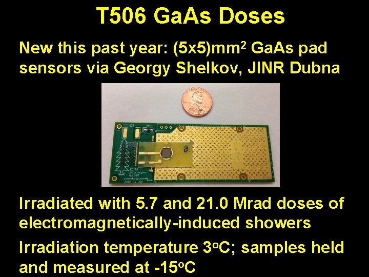
T 506 Ga. As Doses New this past year: (5 x 5)mm 2 Ga. As pad sensors via Georgy Shelkov, JINR Dubna Irradiated with 5. 7 and 21. 0 Mrad doses of electromagnetically-induced showers Irradiation temperature 3 o. C; samples held 14 and measured at -15 o. C

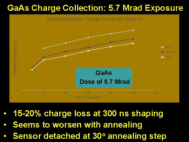
Ga. As Charge Collection: 5. 7 Mrad Exposure Ga. As Dose of 5. 7 Mrad • 15 -20% charge loss at 300 ns shaping • Seems to worsen with annealing • Sensor detached at 30 o annealing step 15

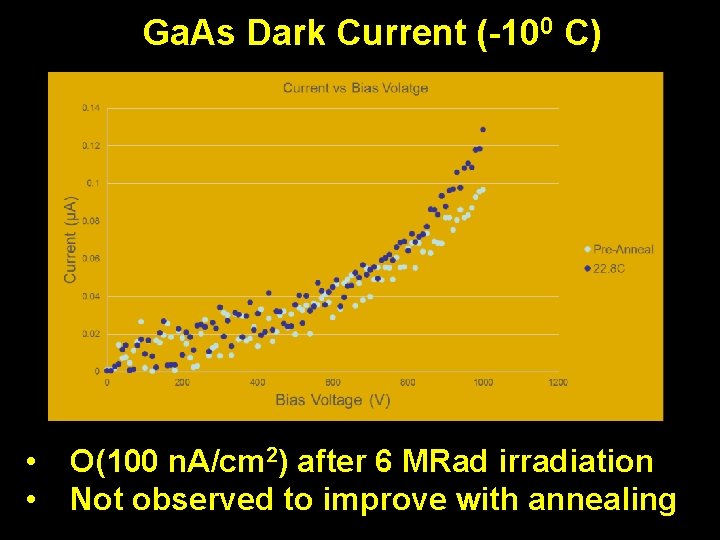
Ga. As Dark Current (-100 C) • • O(100 n. A/cm 2) after 6 MRad irradiation 16 Not observed to improve with annealing

Radiation Damage Plans/Opportunities • Silicon sensor studies to high dose, careful monitoring/control of currents, annealing • Further sensor types (Ga. As, Sapphire, Si. C) • Instrumentation support (FPGA, analysis software) • Silicon sensor for prototype FCAL (ongoing CERN/DESY testbeam studies) 17

Beam. Cal Simulation Efforts 18

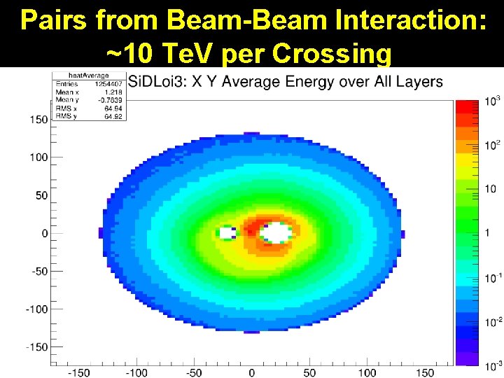
Pairs from Beam-Beam Interaction: ~10 Te. V per Crossing 19

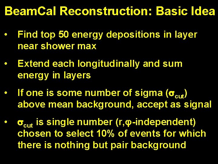
Beam. Cal Reconstruction: Basic Idea • Find top 50 energy depositions in layer near shower max • Extend each longitudinally and sum energy in layers • If one is some number of sigma ( cut) above mean background, accept as signal • cut is single number (r, φ-independent) chosen to select 10% of events for which there is nothing but pair background 20

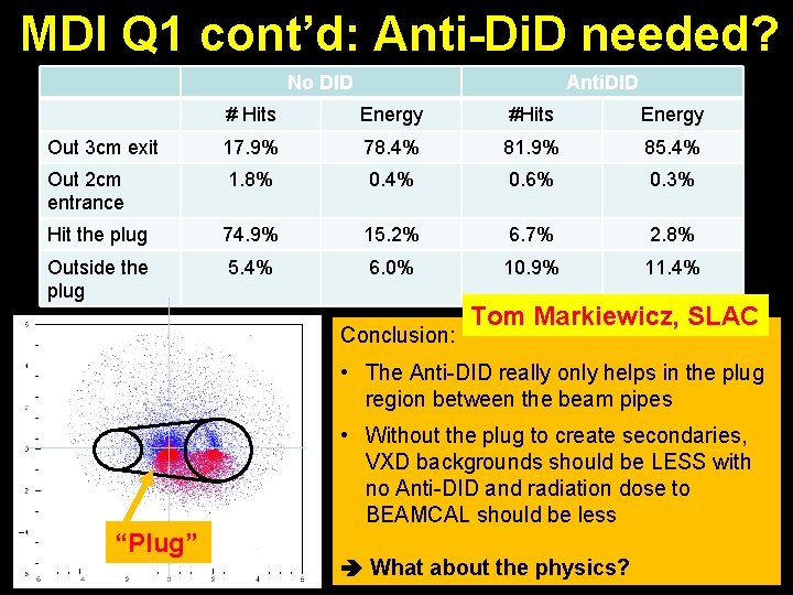
Sample Study: Value of Anti. D N. B. : “No DID” really means “No Anti DID” Tom Markiewicz, SLAC 21

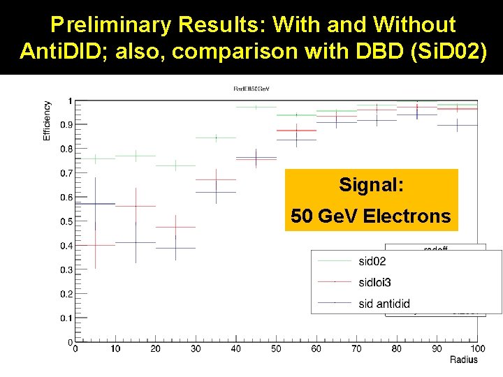
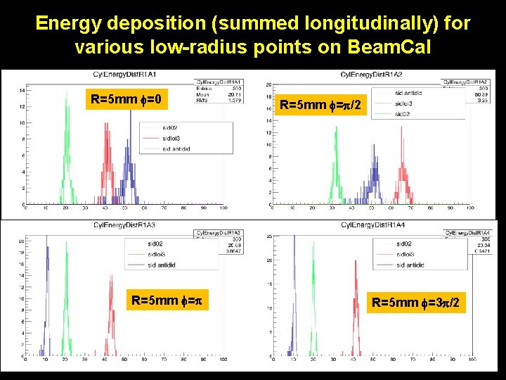
Preliminary Results: With and Without Anti. DID; also, comparison with DBD (Si. D 02) Signal: 50 Ge. V Electrons 22

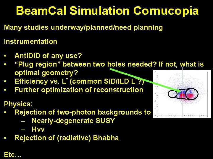
Beam. Cal Simulation Cornucopia Many studies underway/planned/need planning Instrumentation • • Anti. DID of any use? “Plug region” between two holes needed? If not, what is optimal geometry? Efficiency vs. L* (common Si. D/ILD L*? ) Further optimization of reconstruction Physics: • Rejection of two-photon backgrounds to – Nearly-degenerate SUSY – Hνν • Rejection of (radiative) Bhabha Etc… 23

Si. D Beam. Cal “Opportunties” Many areas of ongoing work that offer opportunities for increased effort and collaboration • BEAN chip development (contact Angel Abusleme) • T 506 • Simulations • Or: whatever you see as relevant and of interest Talk to us Attend next FCAL collaboration meeting DESY Zeuthen 20 -21 October If this machine moves forward, we are going 24 to need to really focus seriously on design.

Backup 25

MDI Q 1 cont’d: Anti-Di. D needed? No DID Anti. DID # Hits Energy #Hits Energy Out 3 cm exit 17. 9% 78. 4% 81. 9% 85. 4% Out 2 cm entrance 1. 8% 0. 4% 0. 6% 0. 3% Hit the plug 74. 9% 15. 2% 6. 7% 2. 8% Outside the nn plug 5. 4% 6. 0% 10. 9% 11. 4% Conclusion: Tom Markiewicz, SLAC • The Anti-DID really only helps in the plug region between the beam pipes • Without the plug to create secondaries, VXD backgrounds should be LESS with no Anti-DID and radiation dose to BEAMCAL should be less “Plug” What about the physics? 26

Energy deposition (summed longitudinally) for various low-radius points on Beam. Cal R=5 mm =0 R=5 mm = /2 R=5 mm =3 /2 27

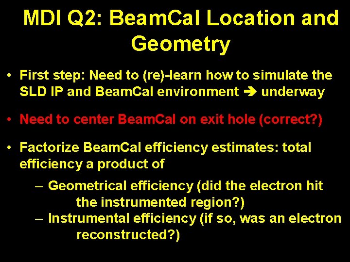
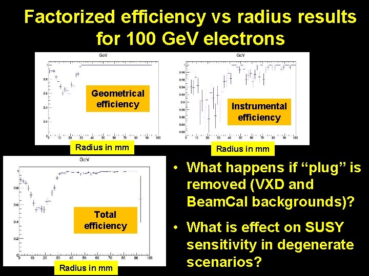
MDI Q 2: Beam. Cal Location and Geometry • First step: Need to (re)-learn how to simulate the SLD IP and Beam. Cal environment underway • Need to center Beam. Cal on exit hole (correct? ) • Factorize Beam. Cal efficiency estimates: total efficiency a product of – Geometrical efficiency (did the electron hit the instrumented region? ) – Instrumental efficiency (if so, was an electron reconstructed? ) 28

Factorized efficiency vs radius results for 100 Ge. V electrons Geometrical efficiency Radius in mm Instrumental efficiency Radius in mm • What happens if “plug” is removed (VXD and Beam. Cal backgrounds)? Total efficiency Radius in mm • What is effect on SUSY sensitivity in degenerate 29 scenarios?

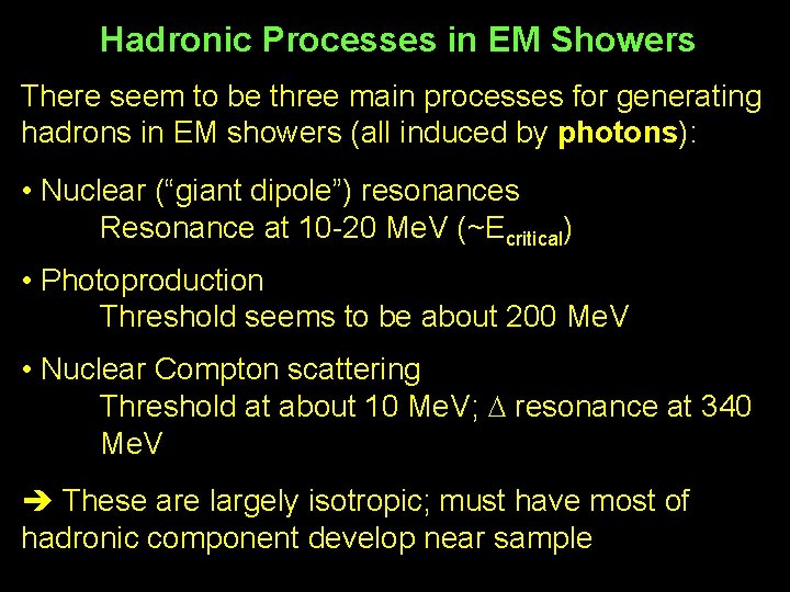
Hadronic Processes in EM Showers There seem to be three main processes for generating hadrons in EM showers (all induced by photons): • Nuclear (“giant dipole”) resonances Resonance at 10 -20 Me. V (~Ecritical) • Photoproduction Threshold seems to be about 200 Me. V • Nuclear Compton scattering Threshold at about 10 Me. V; resonance at 340 Me. V These are largely isotropic; must have most of hadronic component develop near sample 30

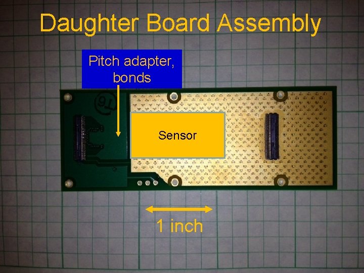
Daughter Board Assembly Pitch adapter, bonds Sensor 1 inch 31

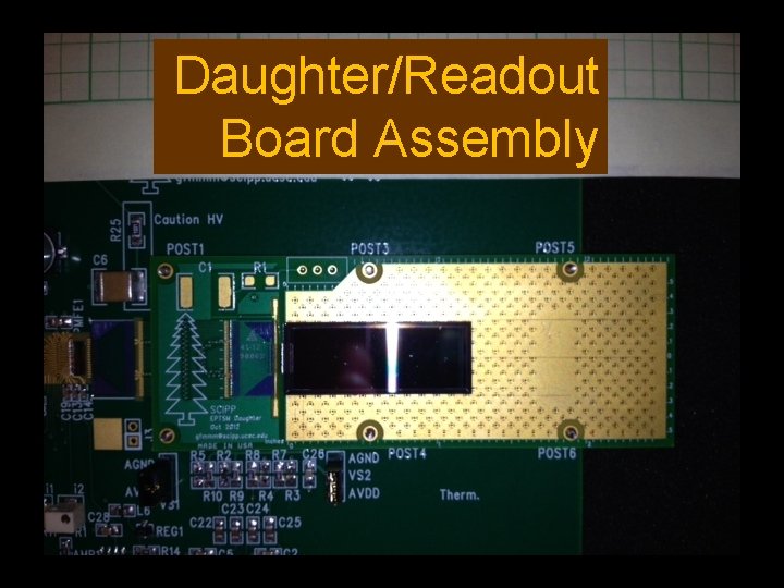
Daughter/Readout Board Assembly 32

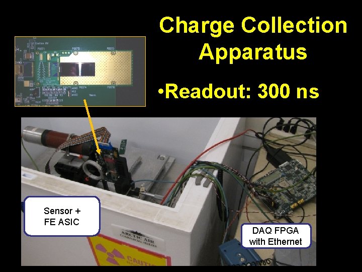
Charge Collection Apparatus • Readout: 300 ns Sensor + FE ASIC DAQ FPGA with Ethernet 33

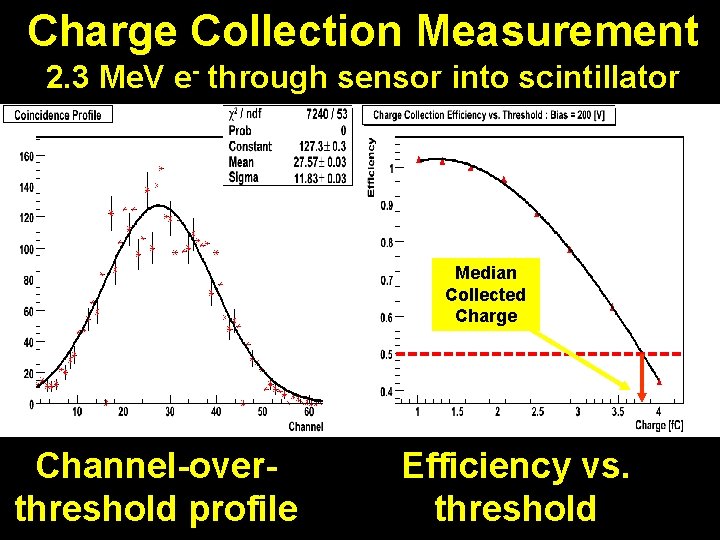
Charge Collection Measurement 2. 3 Me. V e- through sensor into scintillator Median Collected Charge Channel-overthreshold profile Efficiency vs. threshold 34

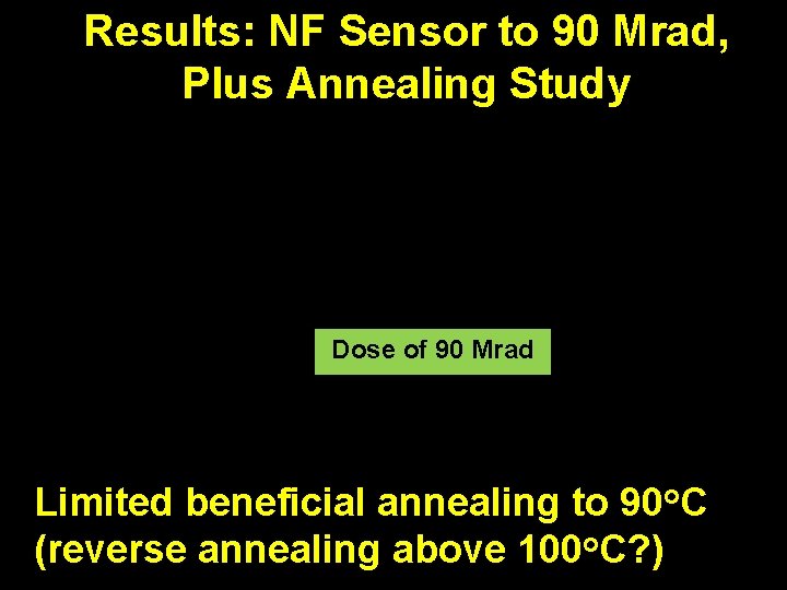
Results: NF Sensor to 90 Mrad, Plus Annealing Study Dose of 90 Mrad Limited beneficial annealing to 90 o. C (reverse annealing above 100 o. C? ) 35

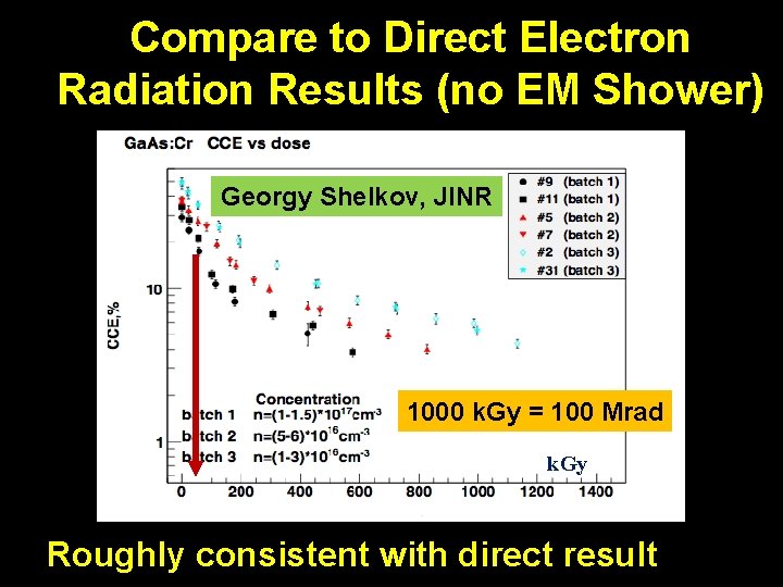
Compare to Direct Electron Radiation Results (no EM Shower) Georgy Shelkov, JINR 1000 k. Gy = 100 Mrad k. Gy Roughly consistent with direct result 36

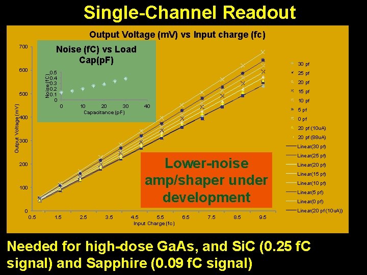
Single-Channel Readout Output Voltage (m. V) vs Input charge (fc) 700 Noise (f. C) vs Load Cap(p. F) Noise (f. C) 600 Output Voltage (m. V) 500 30 pf 0. 5 0. 4 0. 3 0. 2 0. 1 0 25 pf 20 pf 15 pf 0 400 10 20 30 Capacitance (p. F) 10 pf 40 5 pf 0 pf 20 pf (10 u. A) 20 pf (88 u. A) 300 Linear(30 pf) Lower-noise amp/shaper under development 200 100 Linear(25 pf) Linear(20 pf) Linear(15 pf) Linear(10 pf) Linear(5 pf) Linear(0 pf) Linear(20 pf (10 u. A)) 0 0. 5 1. 5 2. 5 3. 5 4. 5 5. 5 Input Charge (fc) 6. 5 7. 5 8. 5 9. 5 Needed for high-dose Ga. As, and Si. C (0. 25 f. C signal) and Sapphire (0. 09 f. C signal)

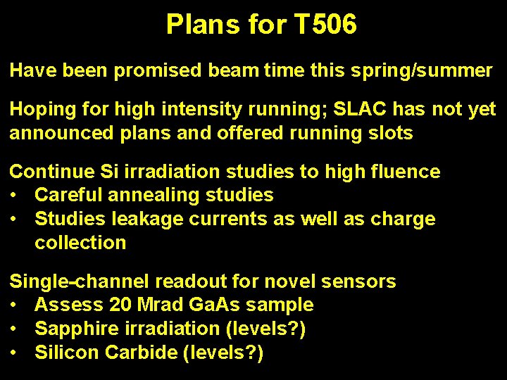
Plans for T 506 Have been promised beam time this spring/summer Hoping for high intensity running; SLAC has not yet announced plans and offered running slots Continue Si irradiation studies to high fluence • Careful annealing studies • Studies leakage currents as well as charge collection Single-channel readout for novel sensors • Assess 20 Mrad Ga. As sample • Sapphire irradiation (levels? ) • Silicon Carbide (levels? ) 38

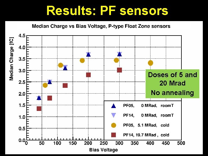
Results: PF sensors Doses of 5 and 20 Mrad No annealing 39

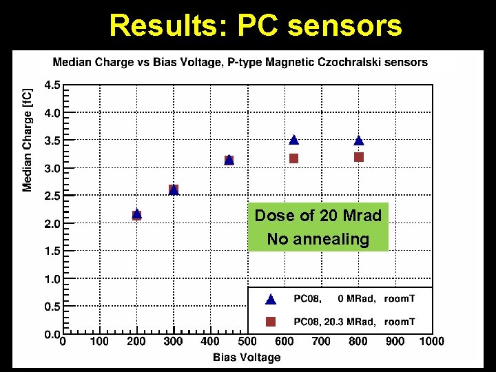
Results: PC sensors Dose of 20 Mrad No annealing 40

Results: NF sensor for low dose Doses of 5 and 20 Mrad No annealing 41