DMT 121 ELECTRONIC DEVICES DIODES TRANSISTOR INTEGRATED CIRCUITS

 ELECTRONIC DEVICES made of SEMICONDUCTOR MATERIAL List 2 common")


")

 that")


, England discovered the electron and developed")
, Denmark - stated that the electrons moved around the")


 (a) Silicon atom Core (+1) (a) Copper atom Diagrams of")

 Covalent bonding of an intrinsic Si crystal (b) Covalent bonding of Ga. As")


 At intrinsic (pure) silicon at room temperature has sufficient")


 device that acts as an one-way")


 when forward biased,")


 is included and the forward dynamic resistance")


 consists of the barrier potential voltage plus the small voltage drop")
Determine the forward voltage and forward current for the diode in Figures")
- Slides: 83
DMT 121 ELECTRONIC DEVICES
DIODES TRANSISTOR INTEGRATED CIRCUITS (IC) ELECTRONIC DEVICES made of SEMICONDUCTOR MATERIAL List 2 common semiconductor materials SILICON GERMANIUM
• Electronic devices such as diodes, transistor and IC are made of a semiconductive material. • To understand how these devices work, you should have a basic knowledge of the structure of atoms and the interaction of atomic particles. • PN junction is fundamental to the operation of devices such as solar cell, diode and certain type of transistor.
Introduction to Semiconductor
Introduction to Semiconductor Define, illustrate and explain the atomic structures, semiconductors, insulators and covalent bonds. Describe the conduction in semiconductor, n-type and p-type semiconductor. Define diode. Explain diode operation and biasing. Solve voltage and current characteristics of various diode models.
Topics Atomic Structure Insulator, Semiconductor, Conductor Current in semiconductors The p-n junction The structure of the diode Biasing a Diode I-V characteristic Diode Models Testing a Diode
is the smallest particle of an element that retains the characteristics of that element.
ATOM Consist of ELECTRONS PROTONS NEUTRONS
The Atom An atom consists of the and that make up the nucleus (core) at the center and electrons that orbit about the nucleus. • The nucleus carries almost the total mass of the atom. • Neutrons are neutral and carry. • Protons carry. • The electrons carry _ . The number of protons the number of electrons in an atom, which makes it electrically neutral or balanced. Bohr model of an atom
Valence Shell is the outermost shell in an atom that determines the Shells or conductivity of anorbital paths atom. The electrons in valence shell are called. - - - N M L - - K - - - 29 p - - - + - - - 29 n - - - Valence shell - - Valenc e electron Bohr model of copper atom (Cu)
Maximum Number of Electrons in Each Shell The maximum number of electron (Ne) that can exist in each shell of an atom is a fact Of nature and can be calculated by the formula, Ne 2 n 2 1 st shell (K): 2 n 2 = 2(1)2 = 2 electrons 2 nd shell (L): 2 n 2 = 2(2)2 = 8 electrons 3 rd shell (M): 2 n 2 = 2(3)2 = 18 electrons 4 th shell (N): 1 electrons Total: n = the shell number 29 electrons
• The periodic table is a table of the chemical elements, showing the symbols for the elements, their full names, their atomic numbers and their mass number. • It organizes them into groups and periods (columns and rows) based on their structure and properties. • It is called "the periodic table" because the horizontal rows are named "periods. "
The Periodic Table of Elements
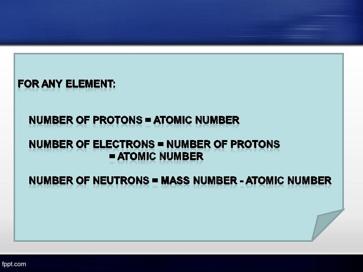
Name: Copper Symbol: Cu Atomic number: 29 Atomic weight: 63. 546 For copper: • Number of Protons = Atomic Number = 29 • Number of Electrons = Number of Protons = Atomic Number = 29 • Number of Neutrons = Mass Number - Atomic Number = 64 - 29 = 35
Timeline of atom • J. J Thomson (1898), England discovered the electron and developed the plum-pudding model of the atom. • Ernest Rutherford (1909), England - used the results of his gold-foil experiment to state that all the mass of an atom were in a small positively-charged ball at the center of the atom.
• Neils Bohr (1913), Denmark - stated that the electrons moved around the nucleus in successively large orbits. He also presented the Bohr atomic model which stated that atoms absorb or emit radiation only when the electrons abruptly jump between allowed, or stationary, states. • Erwin Shroedinger (1926), Austria introduced the Shroedinger Equation, a wave equation that describes the form of the probability waves that govern the motion of small particles and how these waves are altered by external influences.
Electron contents of shells and subshells of the copper atom Shell K (n = 1) L (n = 2) M (n = 3) N (n = 4) Subshells Capacity (2 n 2) Content s 2 2 p 6 6 d 10 10 s 2 1 p 6 0 d 10 0 f 14 0
Insulator, Conductor and Semiconductor Insulators A material that does not conduct electrical current under normal conditions. Valence electrons are tightly bound to the atoms → very few free electrons. Most good insulators are compounds rather than single-elemet materials. Example : rubber, plastics, glass, mica, and quartz.
Conductors A material that easily conducts electrical current. Valence electrons are very loosely bound to the atoms→many free electrons. Characterized by atoms with only one valence electron. The best conductors are single-element materials. Example. : copper, silver, gold and aluminum.
Semiconductor A semiconductors is a material that is between conductor and insulator in its ability to conduct electrical current. Play a significant role in the development of modern electronic device such as diodes, transistors, and integrated circuits. Class of semiconductor : - Single-crystal : Ge, Si & C - - - Compound : Ga. As, Cd. S & Ga. As. P - - Ge - - Si - - - Semiconductor atoms -
Energy Bands Valence shell of an atom represent a band of energy level that contains valence electrons. When an electron have enough additional energy, it can leave the valence shell to become a free electron and exist in conduction band. The energy gap is the difference between the valence band conduction band. This is the amount of energy that a valence electron must have to jump form valence band to conduction band. In conduction band, electron is free to move throughout the material and is not tied to any atom.
Atomic Structure
Energy Level Energy levels: conduction and valence bands of an insulator, a semiconductor, and a conductor.
Energy band diagrams for three different materials The amount of energy that the valence electrons must attain to be elevated to the next level (conduction band) is measured in electron volts (1 e. V = 1. 6 x 10 -19 joules), which is the energy gap between valence band conduction band.
Comparison of a Semiconductor Atom to a Conductor Atom Core of Si atom has a net charge of +4 (14 protons – 10 electrons) and core Cu has a net charge of +1 (29 protons – 28 electrons). The core includes everything except the valence electron. A valence electron in Si atom feels an attractive force of +4 compared to Cu atom which feels an attractive force of +1. The distance from its nucleus of Copper’s valence electron (in 4 th shell) > silicon’s valence electron (in 3 rd shell).
Valence electrons Core (+4) (a) Silicon atom Core (+1) (a) Copper atom Diagrams of the silicon and copper atoms
Covalent Bonds Covalent bonding is the method by which atoms complete their valence shells by “sharing” valence electrons. - - + The results of this bonding are: - - + + - - + 1. The atoms are held together, forming a solid substance. + 2. The atoms are all electrically stable, because their valence shells Covalent bonding in a semiconductor are complete. crystal 3. The completed valence shells cause the atom to act as an insulator.
(a) Covalent bonding of an intrinsic Si crystal (b) Covalent bonding of Ga. As crystal Covalent bonding in (a) Si and (b) Ga. As crystal This bonding of atoms, strengthened by the sharing of electrons, is called covalent bonding
the pure semiconductor, in which the number of free electrons equals the number of holes in the crystal structure. the impure semiconductor that has been doped with n-type or p-type impurity atoms, resulting in imbalance between the hole and electron densities.
Current in Semiconductor Energy Conduction band Energy gap E 4 = 1. 8 e. V E 3 = 0. 7 e. V Conduction band E 2 E 1 Valence band E = energy level Second band (shell 2) Valence band First band (shell 1) Energy band diagram for an unexited atom in a pure (intrinsic) Si crystal. Nucleus
Conduction Electrons and Holes (a) At intrinsic (pure) silicon at room temperature has sufficient heat (thermal) energy for some valence electrons to jump from valence band to conduction band. When an electron jumps to the conduction band, a vacancy is left in the valence band. For every electron raised to the conduction band by external energy, there is one hole left in valence band, creating an electron-hole pair. Recombination occurs band electron loss into a hole in the valence band. its when energy (b) a and conductionfalls back The energy given up by the electron is in the form of light and/or heat. Creation of electron-hole pairs in a Si atom. (a) energy diagram, and (b) bonding diagram
• At the temperature room, at any instant, a number of free electrons that are unattached to any atom drift randomly throughout the material. This condition occurs when no voltage is applied across a piece of intrinsic Si. Free electrons are being generated continuously while some recombine with holes
Electron and Hole Current When a voltage is applied across the piece of intrinsic Si, thermally generated free electrons in the conduction band, which are free to move, are now easily attracted toward the positive end. The movement of free electrons in a semiconductive material is called electron current. At the same time, there also an equal number of holes in the valence band created by electrons that jump into the conduction band. The hole has moved from place to another in crystal structure. The current in valence band is produced by valence electrons is called hole current.
Free electrons are attracted toward the positive end Hole current in intrinsic Si
PN Junction Few terms and processes that are frequently referred to in p-n junction theory Terms/Processes Doping Definitions the process of adding impurity atoms to the intrinsic semiconductor in order to alter the balance between holes and electrons (or to increase the conductivity of the semiconductor). N-type impurities (donor) the type of impurities that add (donate) electrons to intrinsic semiconductors, when combined. P-type impurities (acceptors) the type of impurities that produce holes (accept electrons) in intrinsic semiconductors, when combined.
Few terms and processes that are frequently referred to in p-n junction theory Terms/Processes Ionization Diffusion current Definitions the process of losing or gaining a valence electron. If a neutral atom loses a valence electron, it is no longer neutral and is called a positive ion. On the other hand, if a neutral atom gains a valence electron, it is called a negative ion. results when there is a non-uniform concentration of charge carriers (electrons or holes) in the semiconductor; that is, if there is a higher density of carriers in one region and lower density in another, carriers start migrating from the region of higher density to the region with lower density until a fairly uniform concentration is established in the semiconductor. The flow of these charge carriers during migration constitutes a current flow called diffusion current, and the carriers are said to diffuse from one region to another.
Extrinsic materials • A semiconductor material that has been subjected to the doping process is called an extrinsic material. • Type of materials – n-type – p-type
N-type semiconductor An n-type semiconductor is produced when the intrinsic semiconductor is doped with n-type impurity atoms that have five valence electrons (pentavalent), such as arsenic (As), antimony (Sb), Bismuth (B) and phosphorus (P). Pentavalent atom is called a donor atom. - - - Si - - P - Conduction band Si - Energy - - Excess covalent bond electron - - - - Electrons (majority carriers) Valence band Si - - N-type semiconductor. Four of P atom’s valence electrons are used to form the covalent bond with Si atoms, leaving one extra electron Holes (minority carriers) Energy diagram (n-type semiconductor)
P-type Semiconductor A p-type semiconductor is produced when the intrinsic semiconductor is doped with p-type impurity atoms that have three valance electrons (trivalent), such as aluminum (Al), boron (B), and gallium (Ga). Trivalent atom is referred to as an acceptor atom. - - - B - - Si - Conduction band Si - Energy - - - Covalent bond hole - - - - Electrons (minority carriers) Valence band - Si - - - P-type semiconductor. Three of B atom’ valence electrons are used in the covalent bonds, leaving one hole Holes (majority carriers) Energy diagram (p-type semiconductor)
P type semiconductor Si crystal doped with trivalent atoms such Boron, Antimony, etc. Has majority of “holes”. N type semiconductor Si crystal doped with pentavalent such as Phosporous, Atsenic, etc. Has majority of “electron”.
Formation of PN-junction If a piece of intrinsic silicon is doped so that part is n-type and other part is p-type, a p-n junction forms at the boundary between the two region and a diode is created At instant junction formation, free electrons in the n region near the p-n junction begin to diffuse across the junction and fall into holes near the junction in p region
Formation of Depletion region • • • When the p-n junction is formed – n region loses electron (diffuse across junction) and creates a layer of positive charges near the junction. As electron moves across the junction, p region loses hole as the electron and holes combine. This create a layer of negative charges near the junction. These two layers form the depletion region. Depletion refer to region near the p-n junction is depleted of charge carrier (electrons and holes) due to diffusion across junction. For every free electron that diffuse across the junction and combines with a hole, a positive charge is created in p region, forming a barrier potential. This action continues until the voltage of the barrier prevent further diffusion.
- - - - +4 - - +3 +4 - - +4 - Total (+) = 19 Total (-) = 20 Net charge = -1 Depletion layer charges - - - +5 - - +4 +4 N-type Junction P-type - - +4 - Total (+) = 21 Total (-) = 20 Net charge = +1 -
Each electron that diffuses across the junction leaves one positively charged bond in the n-type material and produces one negatively charged bond in the p-type material. Both conduction-band electrons and valence-band holes are need for conduction through the materials. When an electron diffuses across the junction, the n-type material has lost a conduction-band electron. When the electron falls into a hole in the p-type material, that material has lost a valence-band hole. At this point, both bonds have been depleted of charge carriers.
Energy diagram of PN junction and Depletion Region The valance and conduction band in n-type material are slightly lower than the p-type material, but there is a significant amount of overlapping. The free electron in n-region of the conduction band can easily diffuse across the junction and temporarily become free electrons in the lower part of the p-region conduction band. After crossing the junction, the electrons quickly lose energy and fall into the holes in the pregion valance band.
Energy diagram of PN junction and Depletion Region As the diffusion continues, the depletion region begins to form and the energy level of the n-region conduction band decreases. The decrease in the energy level is due to the loss of the higher-energy electron that have diffused across the junction to the p-region. Soon, there is no electron left in the n-region conduction band with enough energy to across the junction to the p-region. At this point, the junction is at equilibrium, and the depletion region is complete because the diffusion has ceased. The energy level of the n-region conduction band has shifted downward, the energy level of the valance band has also shifted downward.
Bias is a potential applied to p-n junction to obtain certain operating conditions. This potential is used to control the width of the depletion layer. By controlling the width of the depletion layer, we are able to control the resistance of the p-n junction and thus the amount of current that can pass through the device. The relationship between the width of depletion layer and the junction current Depletion Layer Width Junction Resistance Junction Current Minimum Maximum Minimum
Forward Bias Forward bias is a potential used to reduce the resistance of p-n junction or condition that allows current through the p-n junction. A forward-biased p-n junction has minimum depletion layer width and junction resistance. There are two requirements to produce forward bias: The positive side of voltage source (denoted as bias voltage (VBIAS)) is connected to the p-type material of the p-n junction semiconductor and the negative side is connected to the n-type material. Bias voltage (VBIAS) must be greater than the barrier potential. Barrier potential is an energy hill that is created by the electric field between the positive and negative ions in the depletion region on either side of the junction.
resistor limits the forward current to a value that will not damage the device. A p-n junction connected forward bias
PN junction in forward bias The negative side of the bias-voltage source “pushes” the free electrons (the majority carriers in n-type material) toward the p-n junction like charges repel. The negative terminal also provides a continuous flow of electrons into the n region. The free electrons obtain sufficient energy from the biasvoltage to overcome the barrier potential of the depletion region and move on through into the p region. Once in the p region, this free electron have lost too much energy overcoming the barrier potential and thus, the free electrons can’t remain in the conduction band for longer. They immediately combine with holes in valence band.
Since unlike charges attract, the positive side of the biasvoltage source attracts the valence electrons toward the left end of the p region. The holes in the p region provide the medium or pathway for these valence electrons to move through the p region. The valence electrons move from one hole to the next toward the left. The holes, which are the majority carriers in the p region, effectively (not actually) move to the right toward the junction.
A forward-biased p-n junction showing the flow of majority carriers and the voltage due to the barrier potential across the depletion region
Forward bias on depletion region As more electrons flow into the depletion region, the number of positive ions is reduced. As more holes effectively flow into the depletion region on the other side of the p-n junction, the number of negative ions is reduced. This reduction in positive and negative ions during forward bias causes the depletion region to narrow. The depletion region narrows and a voltage drop is produced across the pn- junction when the diode is forward bias.
Barrier potential during forward bias When forward bias is applied, the free electrons have enough energy to overcome the barrier potential and effectively “climb the energy hill” and cross the depletion region. When the free electrons cross the depletion region, they give up an amount of energy equivalent to the barrier potential. The energy loss results in a voltage drop across the p-n junction equal to the barrier potential. An additional small voltage drop occurs across the p and n regions due to the internal resistance of the material. This resistance is called the dynamic resistance. For doped semiconductive material, the dynamic resistance is very small and can usually be neglected.
Summary of Forward Bias Operation
Reverse Bias Reverse bias is a potential that essentially “prevents” current through the diode. A reverse-biased p-n junction has maximum depletion layer width and junction resistance. There are two requirements to produce reverse bias: The positive side of voltage source (denoted as bias voltage) is connected to the n-type material of the p-n junction semiconductor and the negative side is connected to the ptype material. - The depletion region is much wider than in forward bias.
A p-n junction connected for reverse bias.
PN junction in reverse-biased The positive side of the bias-voltage source “pulls” the free electrons (the majority carriers in n-type material) away from the p-n junction. As the electrons flow toward the positive side of the voltage source, additional positive ions are created. This results in a widening of the depletion region and a depletion of majority carriers. In the p region, electrons from the negative side of the voltage source enter as valence electrons and move from hole toward the depletion region where they create additional negative ions. This results in a widening of the depletion region and depletion of majority carriers. As the depletion region widens, the availability of majority carriers decreases. As more of the n and p regions become depleted of majority carriers, the electrical field between the positive and negative ions increases in strength until the potential across the depletion region equals the bias voltage. At this point, the transition current essentially ceases except for a very small reverse current.
The p-n junction during the short transition time immediately after reverse-bias voltage is applied
Reverse Current • There is the extremely small current exists in reverse bias after the transition current dies out. It is caused by the minority carriers in the n and p region that are produced by thermally generated electron-hole pairs. • The small number of free minority electrons in the p region are “pushed” toward the p-n junction by negative bias voltage.
• When these electrons reach the wide depletion region, they “fall down the energy hill” and combine with the minority holes in the n region as valence electrons and flow toward the positive bias voltage, creating a small hole current. • The conduction band in the p region is at a higher energy level than the conduction band in the n region. Therefore, the minority electrons easily pass through the depletion region because they require no additional energy.
The extremely small reverse current in a reversebiased diode is due to the minority carriers from thermally generated electron-hole pairs
Reverse Breakdown Normally, the reverse current is so small that it can be neglected. However, if the external reverse-bias voltage is increased to a value called the breakdown voltage, the reverse current will drastically increase. The small number of free minority electrons in the p region are “pushed” toward the p-n junction by negative bias voltage. When these electrons reach the wide depletion region, they “fall down the energy hill” and combine with the minority holes in the n region as valence electrons and flow toward the positive bias voltage, creating a small hole current. The conduction band in the p region is at a higher energy level than the conduction band in the n region. Therefore, the minority electrons easily pass through the depletion region because they require no additional energy.
Summary of Reverse Bias Condition
Diodes Introduction A diode is a two-electrode (twoterminal) device that acts as an one-way conductor. The p region is called the anode and the n region is called the cathode. The arrow in the symbol points in the direction of conventional current (ID) (opposite to electron flow). VD Anode (A) Cathode (K) + - ID The symbol for the p-n junction diode
VF The most basic type of diode is the p-n junction diode. A diode is forward-biased when the positive terminal of the source is connected to the anode through a currentlimiting resistor and the negative terminal is connected to the cathode. A diode is reverse-biased when the negative terminal of the source is connected to the anode and the positive terminal is connected to the cathode. When forward biased, a pn conducts. junction When reverse biased, it diode effectively blocks the flow of charge (current). - + VBias IF + R - (a) Forward-biased diode VD + VBias - I≈0 + R (b) Reverse-biased diode Two different bias circuits
Diode Models We have three diode models: 1. Ideal Model 2. Practical Model 3. Complete Model
Ideal Diodes The ideal diode behaves like a closed switch (ON) when forward biased, and like an open switch (OFF) when it is reverse biased. VA VA VA IF = 0 IF > 0 VF VK IF VF = 0 VK ON The behavior of the ideal diode can be summarized as following: VF < 0 VK OFF The behavior of the diode: (a) ideal diode, (b) short circuit and (c) open circuit If the diode is ON, current passes from the anode to cathode. Therefore, we can replace it with a close circuit. If the diode is OFF, cathode voltage is greater than anode voltage. Then, we can replace it with an open circuit. Diode ON : IF > 0; VF = 0 → VA = VK Diode OFF: IF = 0; VF < 0 → VA < VK when you are trying This model is adequate for most troubleshooting to determine whether the diode is working properly.
IF Based on the characteristics of a switch, it can be stated that the ideal diode: 1. When reverse biased (open switch): a. The diode has infinite resistance. b. The diode does not pass current. c. The diode drops the applied voltage across its terminals. 2. When forward biased (closed switch): a. The diode has no resistance. b. The diode does not limit the circuit current. c. The diode has no voltage drop across its terminals. Forward operating region VR II I III IV Reverse operating region IR I-V characteristics of the ideal diode VF
Since the barrier potential and the forward dynamic resistance are neglected, the diode is assumed to have a zero voltage across it when forward-biased, as indicated by the portion of the curve on the positive vertical axis in Figure below. VF 0 V The forward current is determined by the bias voltage and the limiting resistor using Ohm’s law: VBias IF Forward Bias RLimit Since the reverse current is neglected, its value is assumed to be zero by the portion of the curve on the negative horizontal axis. IR 0 V The reserve voltage equals the bias voltage. VR VBias Reverse Bias 0
Practical Diodes The practical model includes the barrier potential. When the diode is forward-biased, it is equivalent to a closed switch in series with a small equivalent voltage source (VF) equals to the barrier potential (0. 7) with the positive side toward the anode. This equivalent voltage source represents the barrier potential that must be exceeded by the bias voltage before the diode will conduct and is not an active source of voltage. When the diode is reverse-biased, it is equivalent to an open switch just as in the ideal model. The barrier potential does not affect reverse bias. Since the barrier potential is included and the dynamic resistance is neglected, the diode is assumed to have a voltage across it when forward-bias.
Since the barrier potential (0. 7 V) is included and the forward dynamic resistance are neglected, the voltage across a diode when forward-biased is 0. 7 V VF The forward current is determined as follows by first applying Kirchoff’s voltage law: V V I R Bias F F Limit The diode is assumed to have zero reverse current, as indicated by the portion of the curve on the negative horizontal axis. IR 0 A VR VBias This model is useful to troubleshoot in lower-voltage circuits and to design the
Complete Diode Model The complete model includes the barrier potential, the small forward dynamic resistance (r’ d), and the large internal reverse resistance (r’ ). R When the diode is forwardbiased, it acts as a closed switch in series with the equivalent barrier voltage (VB= 0. 7 V) and the small forward dynamic resistance (r’d) VB
When the diode is reversebiased it is acts as an open switch in parallel with the large internal reverse resistance (r’R), The barrier potential does not affect reverse bias. Since the barrier potential and the dynamic resistance are included, the diode is assumed to have a voltage across it when
The voltage (VF) consists of the barrier potential voltage plus the small voltage drop across the dynamic resistance, as indicated by the portion of the curve to the right of the origin. The curve slops because the voltage drop due to dynamic resistance increases as the current increases. For the complete model of a silicon diode, the following formulas apply: V F 0. 7 V I F rd' VBias 0. 7 V IF R Limit rd' For troubleshooting work, it is unnecessary to use the complete model, because it involves complicated calculations. This model is generally suited to design problems using a computer for simulation.
Exercise 1 (a)Determine the forward voltage and forward current for the diode in Figures below for each of the diode models. Also find the voltage across the limiting resistor in each case. Assume r’d = 10 Ω at the determined value of forward current. (b)Determine the reverse voltage and reverse current for the diode in Fig. 1. 31(b) for each of the diode models. Also find the voltage across the limiting resistor in each case. Assume IR = 1μA. RLimit VBias + - IF RLimit 2 kΩ VBias 10 V + - (a) Forward-biased diode Two different bias circuits IF 2 kΩ 10 V (b) Reverse-biased diode