DMT 2413 INTRODUCTION TO IC LAYOUT Week 10

- Slides: 15
DMT 241/3 INTRODUCTION TO IC LAYOUT Week 10 th: Ideal I-V Characteristic
Outline � Revision MOS operation � IV Characteristic for all region � Calculation
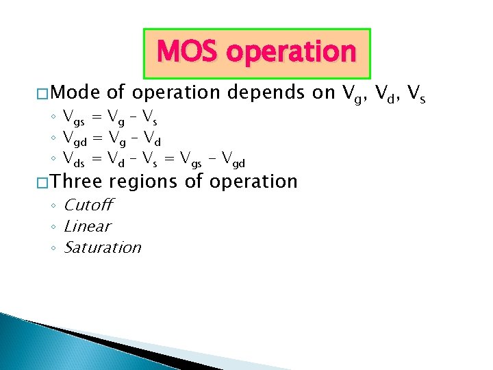
MOS operation �Mode of operation depends on Vg, Vd, Vs �Three regions of operation ◦ Vgs = Vg – Vs ◦ Vgd = Vg – Vd ◦ Vds = Vd – Vs = Vgs - Vgd ◦ Cutoff ◦ Linear ◦ Saturation
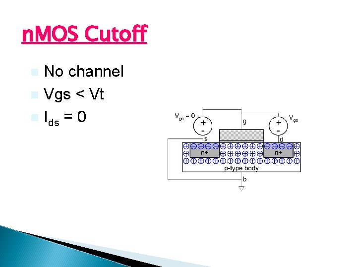
n. MOS Cutoff No channel n Vgs < Vt n Ids = 0 n
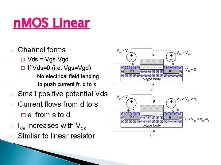
n. MOS Linear n Channel forms Vds = Vgs-Vgd ¨ If Vds=0 (i. e. Vgs=Vgd) ¨ n n n No electrical field tending to push current fr. d to s. Small positive potential Vds Current flows from d to s ¨ e- from s to d Ids increases with Vds Similar to linear resistor
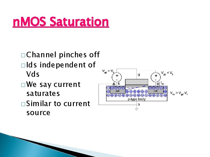
n. MOS Saturation � Channel pinches off � Ids independent of Vds � We say current saturates � Similar to current source
I-V Characteristic for all region � Using 1 st order model (ideal Shockley) � In cutoff region (Vgs < Vt) = no channel and almost zero current flow � Other region, the gate attract carriers (electron) to form a channel. � The electron drift from source to drain at a rate proportional to the electric field between these regions.
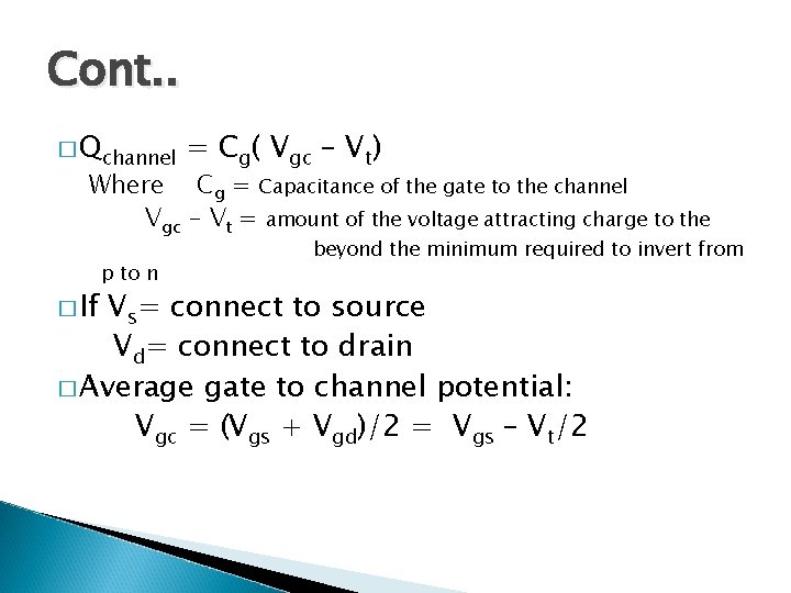
Cont. . � Qchannel = Cg( Vgc – Vt) Where Cg = Capacitance of the gate to the channel Vgc – Vt = amount of the voltage attracting charge to the � If p to n beyond the minimum required to invert from Vs= connect to source Vd= connect to drain � Average gate to channel potential: Vgc = (Vgs + Vgd)/2 = Vgs – Vt/2
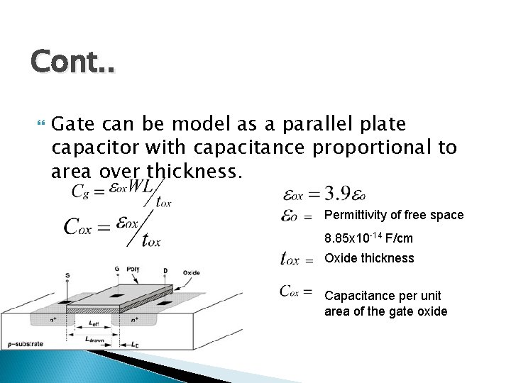
Cont. . Gate can be model as a parallel plate capacitor with capacitance proportional to area over thickness. Permittivity of free space 8. 85 x 10 -14 F/cm Oxide thickness Capacitance per unit area of the gate oxide
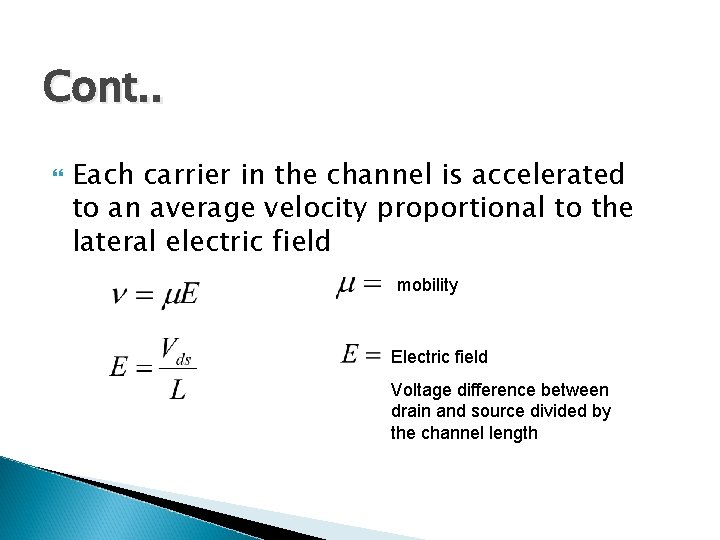
Cont. . Each carrier in the channel is accelerated to an average velocity proportional to the lateral electric field mobility Electric field Voltage difference between drain and source divided by the channel length
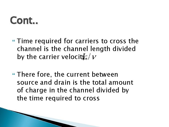
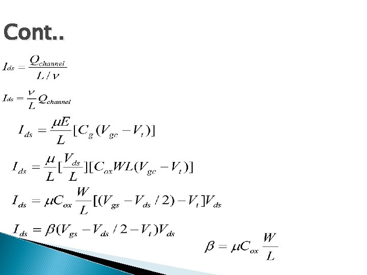
Cont. . Time required for carriers to cross the channel is the channel length divided by the carrier velocity; There fore, the current between source and drain is the total amount of charge in the channel divided by the time required to cross
Cont. .
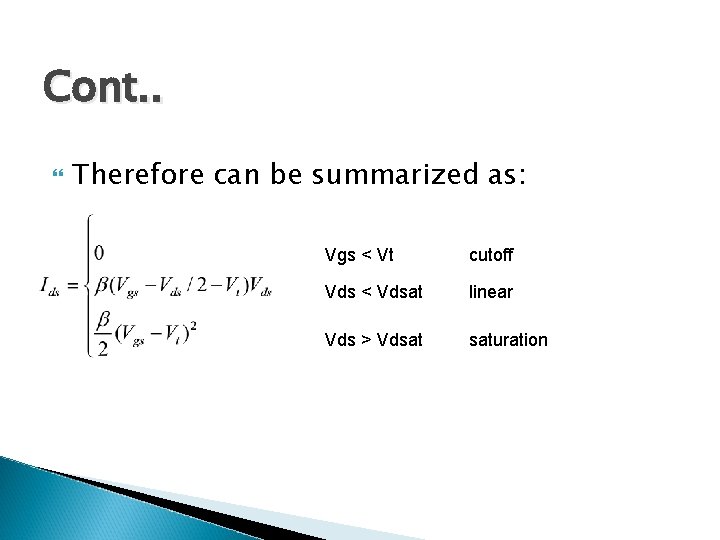
Cont. . Therefore can be summarized as: Vgs < Vt cutoff Vds < Vdsat linear Vds > Vdsat saturation
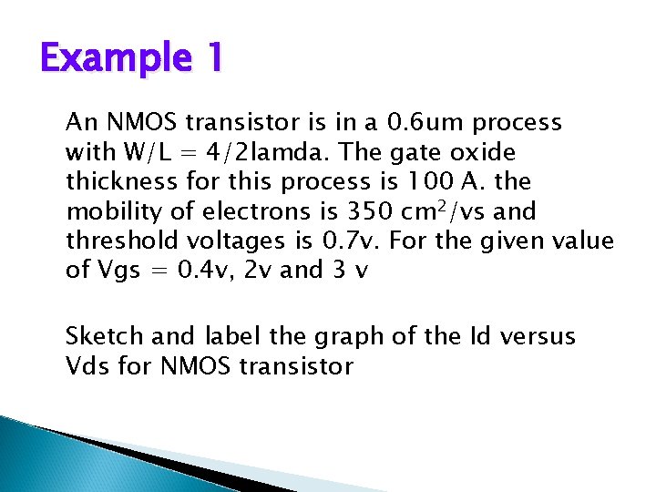
Example 1 An NMOS transistor is in a 0. 6 um process with W/L = 4/2 lamda. The gate oxide thickness for this process is 100 A. the mobility of electrons is 350 cm 2/vs and threshold voltages is 0. 7 v. For the given value of Vgs = 0. 4 v, 2 v and 3 v Sketch and label the graph of the Id versus Vds for NMOS transistor
Example 2: An NMOS transistor in a 180 nm process with W/L = 4/2 lamda. The gate oxide thickness for this process is 40 Å. The mobility of electrons is 180 cm 2/V. s at 80°C and threshold voltages is 0. 4 V. Calculate Capacitance gate oxide. Calculate β. Find IDS when VGS = 0 V, 0. 3 V, 0. 7 V, 1. 2 V, 1. 5 V and 1. 8 V (in saturation region)