
DMT 242 Wafer Fabrication LECTURE 1 INTRODUCTION TO
DMT 242 Wafer Fabrication LECTURE 1 INTRODUCTION TO WAFER FABRICATION This course is basically about silicon chip fabrication, the technologies used to manufacture ICs. Mnorhafiz 2011

DMT 242 Wafer Fabrication What is wafer fabrication? Semiconductor processing facility which turns wafers into Integrated Circuits (ICs). A typical wafer fabrication employs a series of complex steps to define conductors, transistors, resistors, and other electronic components on the semiconductor wafer. The steps are built in the cleanroom includes Oxidation, Photolithography, Etching and Metallization process. Mnorhafiz 2011
INTRO DUCTI ON

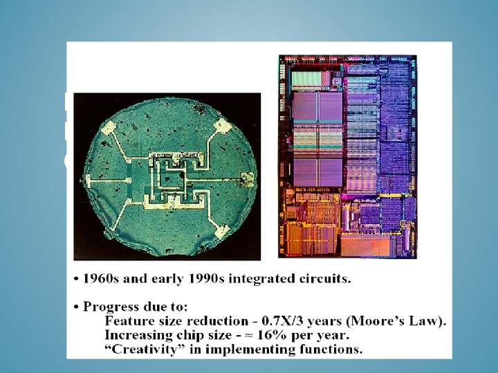
IC FABRICATION TECHNOLOGY: BRIEF HISTORY • 1940 s - the initial inventions that made integrated circuits possible. • In 1945, Bell Labs established a group to develop a semiconductor replacement for the vacuum tube. The group led by William Shockley, included, John Bardeen, Walter Brattain and others. • In 1947 Bardeen and Brattain and Shockley succeeded in creating an amplifying circuit utilizing a point-contact "transfer resistance" device that later became known as a transistor. • In 1951 Shockley developed the junction transistor, a more practical form of the transistor. • By 1954 the transistor was an essential component of the telephone system and the transistor first appeared in hearing aids followed by radios.
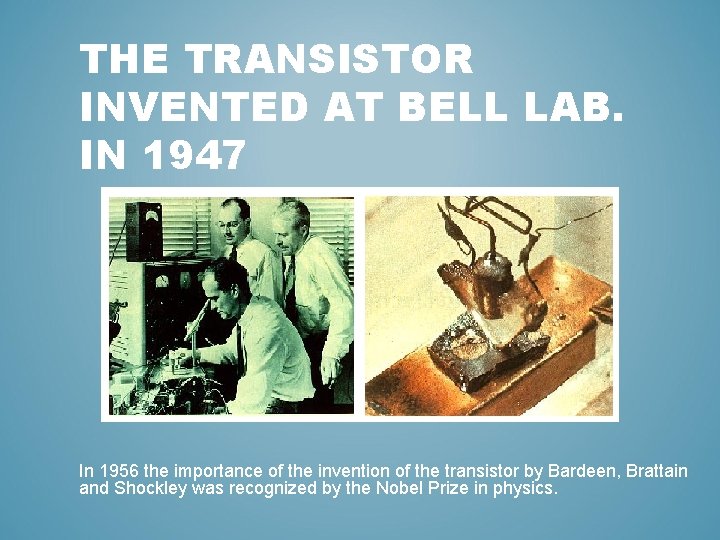
THE TRANSISTOR INVENTED AT BELL LAB. IN 1947 In 1956 the importance of the invention of the transistor by Bardeen, Brattain and Shockley was recognized by the Nobel Prize in physics.
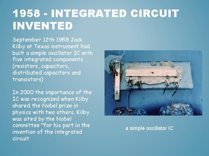
1958 - INTEGRATED CIRCUIT INVENTED September 12 th 1958 Jack Kilby at Texas instrument had built a simple oscillator IC with five integrated components (resistors, capacitors, distributed capacitors and transistors) In 2000 the importance of the IC was recognized when Kilby shared the Nobel prize in physics with two others. Kilby was sited by the Nobel committee "for his part in the invention of the integrated circuit a simple oscillator IC
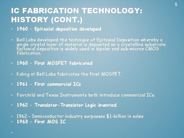
IC FABRICATION TECHNOLOGY: HISTORY (CONT. ) • 1960 - Epitaxial deposition developed • Bell Labs developed the technique of Epitaxial Deposition whereby a single crystal layer of material is deposited on a crystalline substrate. Epitaxial deposition is widely used in bipolar and sub-micron CMOS fabrication. • 1960 - First MOSFET fabricated • Kahng at Bell Labs fabricates the first MOSFET. • 1961 - First commercial ICs • Fairchild and Texas Instruments both introduce commercial ICs. • 1962 - Transistor-Transistor Logic invented • 1962 - Semiconductor industry surpasses $1 -billion in sales • 1963 - First MOS IC • 5
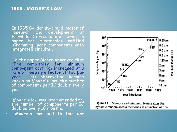
1965 - MOORE'S LAW • In 1965 Gordon Moore, director of research and development at Fairchild Semiconductor wrote a paper for Electronics entitled "Cramming more components onto integrated circuits". • In the paper Moore observed that "The complexity for minimum component cost has increased at a rate of roughly a factor of two per year". This observation became known as Moore's law, the number of components per IC double every year. Moore's law was later amended to, the number of components per IC doubles every 18 months. • Moore's law hold to this day. •
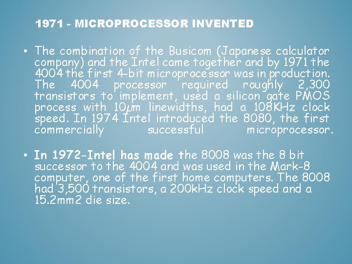
1971 - MICROPROCESSOR INVENTED • The combination of the Busicom (Japanese calculator company) and the Intel came together and by 1971 the 4004 the first 4 -bit microprocessor was in production. The 4004 processor required roughly 2, 300 transistors to implement, used a silicon gate PMOS process with 10µm linewidths, had a 108 KHz clock speed. In 1974 Intel introduced the 8080, the first commercially successful microprocessor. • In 1972 -Intel has made the 8008 was the 8 bit successor to the 4004 and was used in the Mark-8 computer, one of the first home computers. The 8008 had 3, 500 transistors, a 200 k. Hz clock speed and a 15. 2 mm 2 die size.
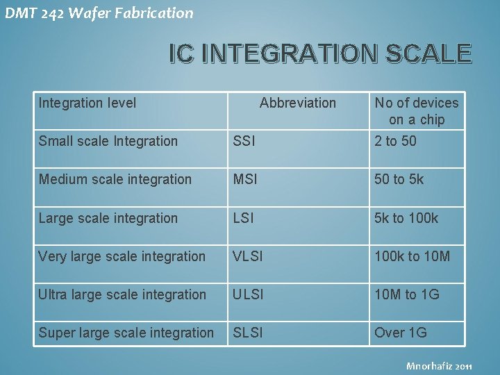
DMT 242 Wafer Fabrication IC INTEGRATION SCALE Integration level Abbreviation No of devices on a chip Small scale Integration SSI 2 to 50 Medium scale integration MSI 50 to 5 k Large scale integration LSI 5 k to 100 k Very large scale integration VLSI 100 k to 10 M Ultra large scale integration ULSI 10 M to 1 G Super large scale integration SLSI Over 1 G Mnorhafiz 2011
DMT 242 Wafer Fabrication CLEANROOM Mnorhafiz 2011

CLEANROOM CLASS 100

ENTERING CLEANROOM

VLSI CLEANROOM

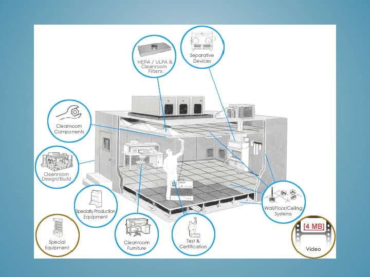
CLEANROOM DESIGN & CONSTRUCTION
DMT 242 Wafer Fabrication Cleanroom • Definition of cleanroom: The cleanliness of the air inside the room or area. The number of particles, humidity and temperature is control according to the standard. • Particles kills yield • IC fabrication must be in a clean room Mnorhafiz 2011
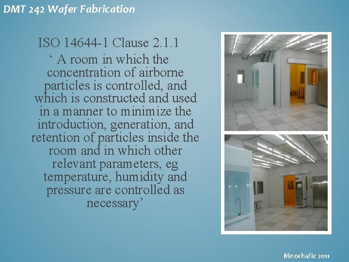
DMT 242 Wafer Fabrication ISO 14644 -1 Clause 2. 1. 1 ‘ A room in which the concentration of airborne particles is controlled, and which is constructed and used in a manner to minimize the introduction, generation, and retention of particles inside the room and in which other relevant parameters, eg temperature, humidity and pressure are controlled as necessary’ Mnorhafiz 2011
DMT 242 Wafer Fabrication Clean room • First used for surgery room to avoid bacteria contamination • Adopted in semiconductor industry in 1950 • Smaller device needs higher grade clean room • Less particle, more expensive to build Mnorhafiz 2011
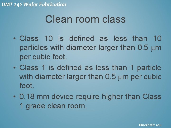
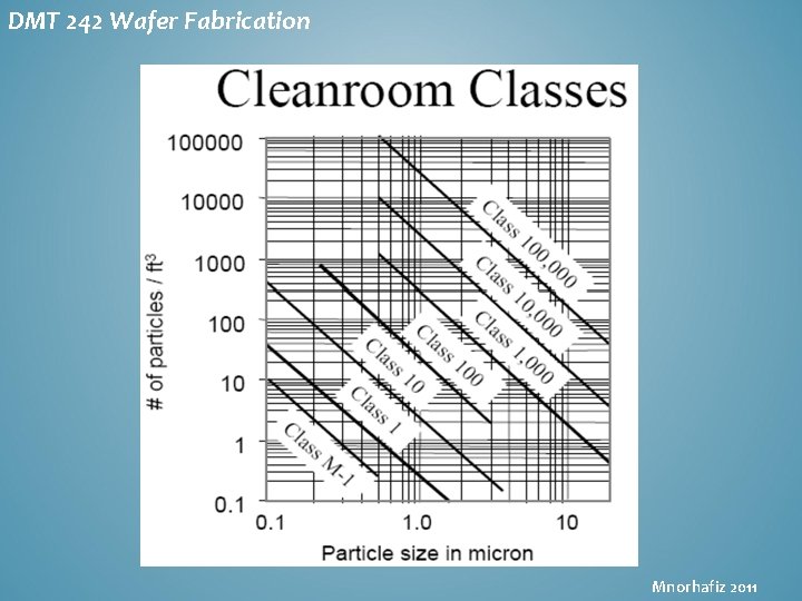
DMT 242 Wafer Fabrication Clean room class • Class 10 is defined as less than 10 particles with diameter larger than 0. 5 m per cubic foot. • Class 1 is defined as less than 1 particle with diameter larger than 0. 5 m per cubic foot. • 0. 18 mm device require higher than Class 1 grade clean room. Mnorhafiz 2011
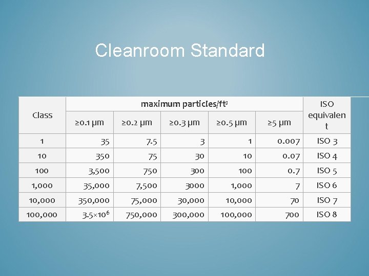
Cleanroom Standard Class maximum particles/ft³ ≥ 0. 1 µm ≥ 0. 2 µm ≥ 0. 3 µm ≥ 0. 5 µm ISO equivalen t ≥ 5 µm 1 35 7. 5 3 1 0. 007 ISO 3 10 350 75 30 10 0. 07 ISO 4 100 3, 500 750 300 100 0. 7 ISO 5 1, 000 35, 000 7, 500 3000 1, 000 7 ISO 6 10, 000 350, 000 75, 000 30, 000 10, 000 70 ISO 7 100, 000 3. 5× 10⁶ 750, 000 300, 000 100, 000 700 ISO 8
DMT 242 Wafer Fabrication Mnorhafiz 2011
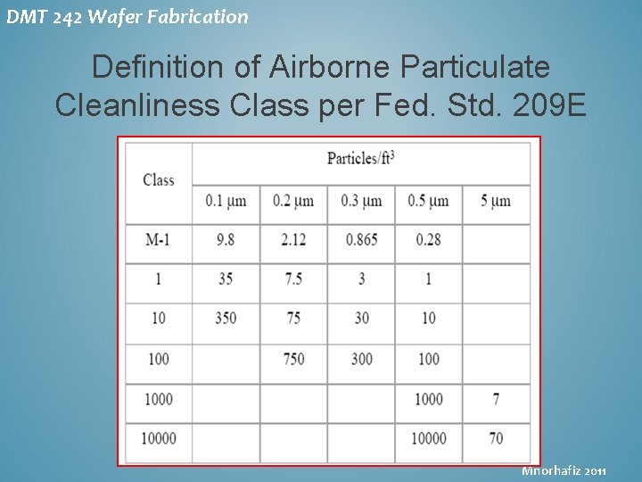
DMT 242 Wafer Fabrication Definition of Airborne Particulate Cleanliness Class per Fed. Std. 209 E Mnorhafiz 2011
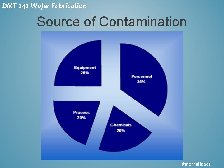
DMT 242 Wafer Fabrication Source of Contamination Mnorhafiz 2011
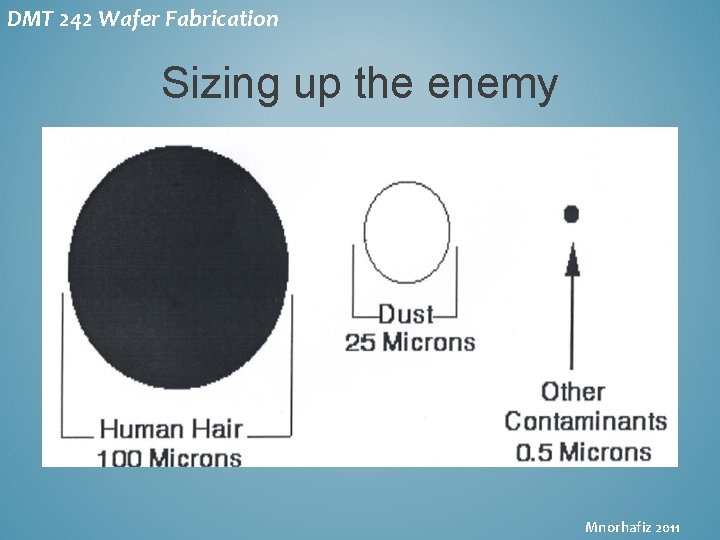
DMT 242 Wafer Fabrication Sizing up the enemy Mnorhafiz 2011
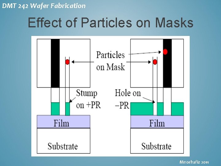
DMT 242 Wafer Fabrication Effect of Particles on Masks Mnorhafiz 2011
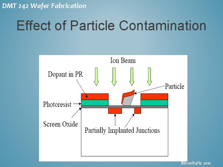
DMT 242 Wafer Fabrication Effect of Particle Contamination Mnorhafiz 2011
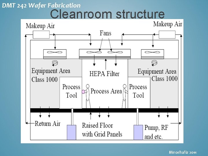
DMT 242 Wafer Fabrication Cleanroom structure Mnorhafiz 2011
DMT 242 Wafer Fabrication CLEANROOM PROTOCOLS Mnorhafiz 2011
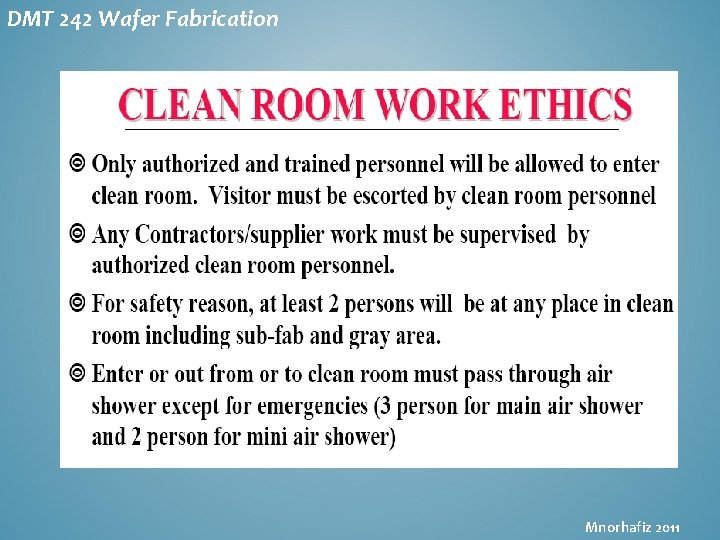
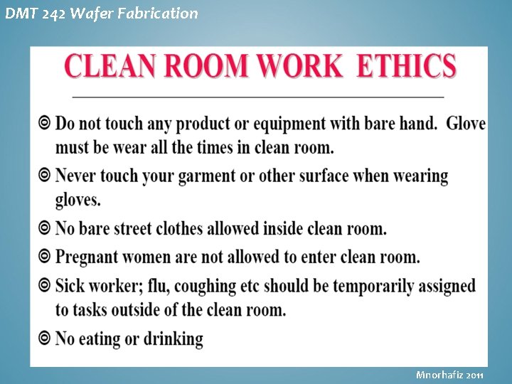
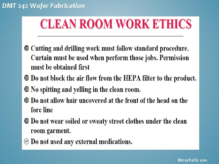
DMT 242 Wafer Fabrication Cleanroom protocols • Cleanroom protocol- A set of rules and procedures that cleanroom workers must follow to maintain the cleanliness of the cleanroom environment. • All cleanroom workers must be trained and certified when they start with, and at least once a year thereafter. • Bunny suits are required for all personnel in the cleanroom at all the times. Bunny suits are effective at containing contamination originating from clothing. Mnorhafiz 2011
DMT 242 Wafer Fabrication Purposes • To ensure the cleanroom procedure is implemented and practiced by all personnel including visitors. • To control and maintain the cleanliness of the cleanroom. • To maintain the good quality of products. • To ensure the safety of personnel and properties. Mnorhafiz 2011
DMT 242 Wafer Fabrication Cleanroom Entry Items • 1. 2. 3. Garments and Booties Blue- Maintenance, facility, contractors White- Process, production, test/PI Green- visitors/vendors Mnorhafiz 2011
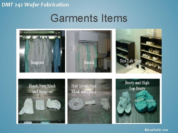
DMT 242 Wafer Fabrication Garments Items Mnorhafiz 2011
DMT 242 Wafer Fabrication Gowning Procedures- Pre Entry • • Change street shoes to clean shoes Visitor must wear shoe cover Enter fab building Remove and place all belongings at designated cabinet • Place clean shoes to shoe rack Mnorhafiz 2011
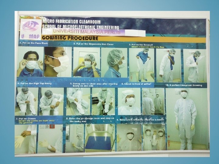
DMT 242 Wafer Fabrication Gowning procedures- Changing room 1. 2. 3. 4. 5. 6. 7. 8. 9. Put on face mask first. Put on disposable hair cover. Put on the jumpsuit. Walk to gowning bench and wear high top booty. Swing over to clean area after wearing booty at one side. Check in front of mirror. Put on gloves. Walk along the tacky mat. Enter main air shower (maximum 3 persons). Make few rotation when air is blown. Wait until air blow stops. Mnorhafiz 2011
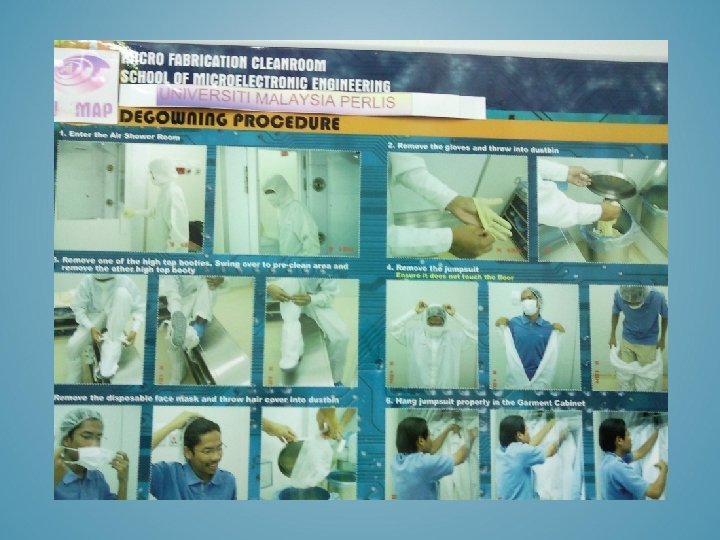
DMT 242 Wafer Fabrication De-gowning Procedure- Changing Room • • Enter air shower (wait until back door closed) Remove gloves and throw into dustbin. Walk to gowning bench. Remove one of high top booty. Swing over to pre-clean area and remove another high top booty. Remove jumpsuit, hood, permanent face mask and hair cover. Hang properly to garment cabinet. Visitor need to remove disposable face mask and hair cover. Thrown into dustbin. Wear clean shoe. Visitor need to remove shoe cover at fab entrance/linkway entrance. Mnorhafiz 2011
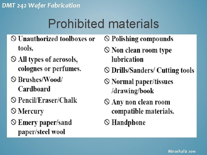
DMT 242 Wafer Fabrication Prohibited materials Mnorhafiz 2011
DMT 242 Wafer Fabrication Mnorhafiz 2011
DMT 242 Wafer Fabrication Mnorhafiz 2011
DMT 242 Wafer Fabrication Mnorhafiz 2011
DMT 242 Wafer Fabrication Mnorhafiz 2011
DMT 242 Wafer Fabrication Mnorhafiz 2011
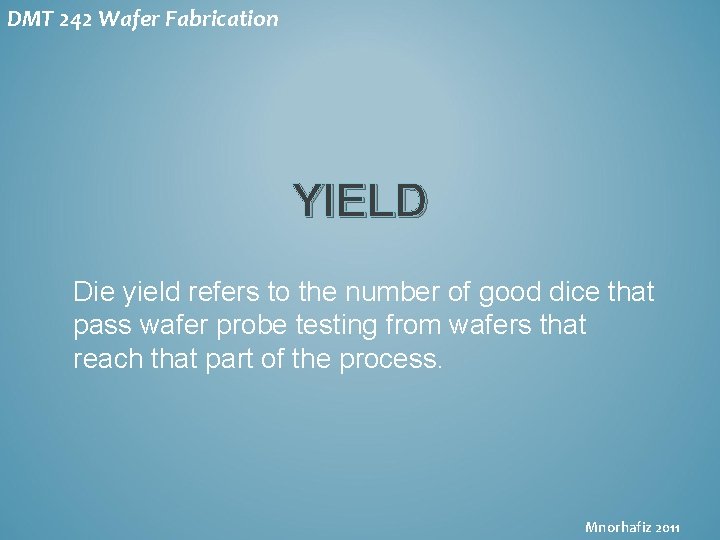
DMT 242 Wafer Fabrication YIELD Die yield refers to the number of good dice that pass wafer probe testing from wafers that reach that part of the process. Mnorhafiz 2011
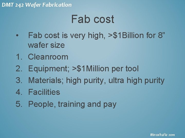
DMT 242 Wafer Fabrication Fab cost • 1. 2. 3. 4. 5. Fab cost is very high, >$1 Billion for 8” wafer size Cleanroom Equipment; >$1 Million per tool Materials; high purity, ultra high purity Facilities People, training and pay Mnorhafiz 2011
DMT 242 Wafer Fabrication Types of Yield 1. Wafer yield 2. Die yield 3. Manufacturing yield Mnorhafiz 2011
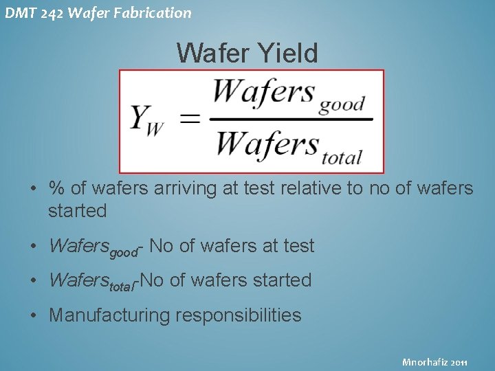
DMT 242 Wafer Fabrication Wafer Yield • % of wafers arriving at test relative to no of wafers started • Wafersgood- No of wafers at test • Waferstotal-No of wafers started • Manufacturing responsibilities Mnorhafiz 2011
DMT 242 Wafer Fabrication Low Wafer Yield • • • Depends mainly on processing and wafer handling. Careless human handling and robot malfunction or miscalibration can break the brittle silicon wafers. Faulty processes such as misaligned photolithography followed with etch or ion implantation, wrong dopant concentration, poor uniformity, or large amounts of particles on wafer can ruin wafers. Mnorhafiz 2011
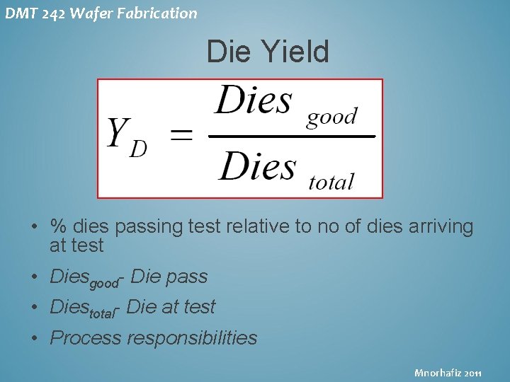
DMT 242 Wafer Fabrication Die Yield • % dies passing test relative to no of dies arriving at test • Diesgood- Die pass • Diestotal- Die at test • Process responsibilities Mnorhafiz 2011
DMT 242 Wafer Fabrication Low Die Yield • Particle contamination, process maintenance, and total process steps. Mnorhafiz 2011
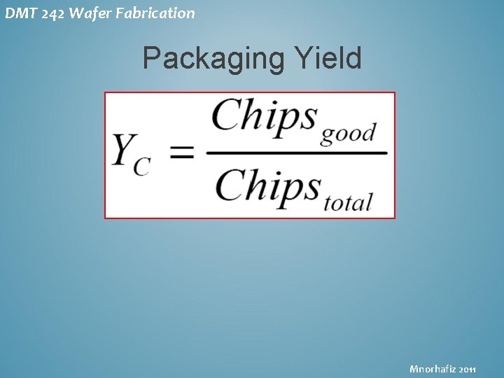
DMT 242 Wafer Fabrication Packaging Yield Mnorhafiz 2011
DMT 242 Wafer Fabrication Low Packaging Yield • Wire bonding quality. • Specification difference between the die test and the chip final test Mnorhafiz 2011
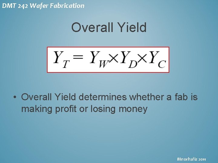
DMT 242 Wafer Fabrication Overall Yield • Overall Yield determines whether a fab is making profit or losing money Mnorhafiz 2011
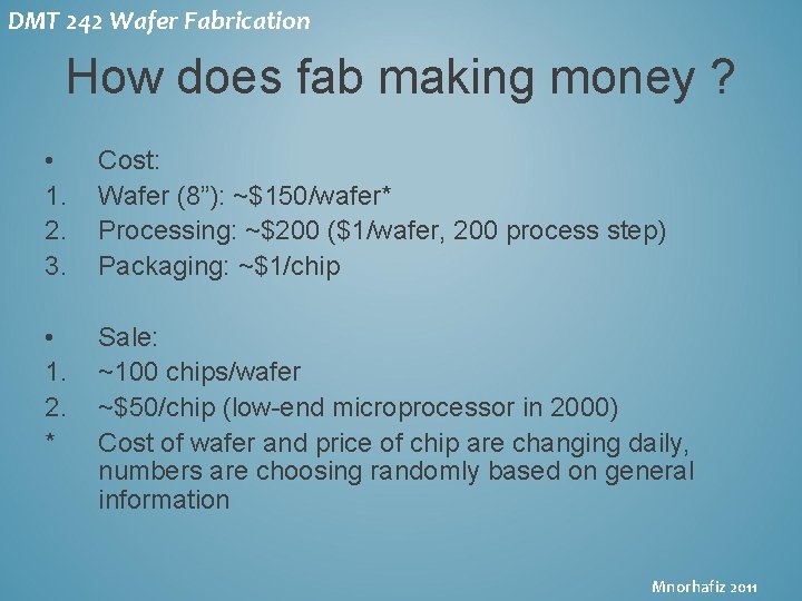
DMT 242 Wafer Fabrication How does fab making money ? • 1. 2. 3. Cost: Wafer (8”): ~$150/wafer* Processing: ~$200 ($1/wafer, 200 process step) Packaging: ~$1/chip • 1. 2. * Sale: ~100 chips/wafer ~$50/chip (low-end microprocessor in 2000) Cost of wafer and price of chip are changing daily, numbers are choosing randomly based on general information Mnorhafiz 2011
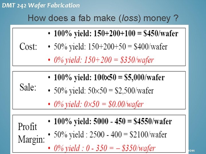
DMT 242 Wafer Fabrication How does a fab make (loss) money ? Mnorhafiz 2011
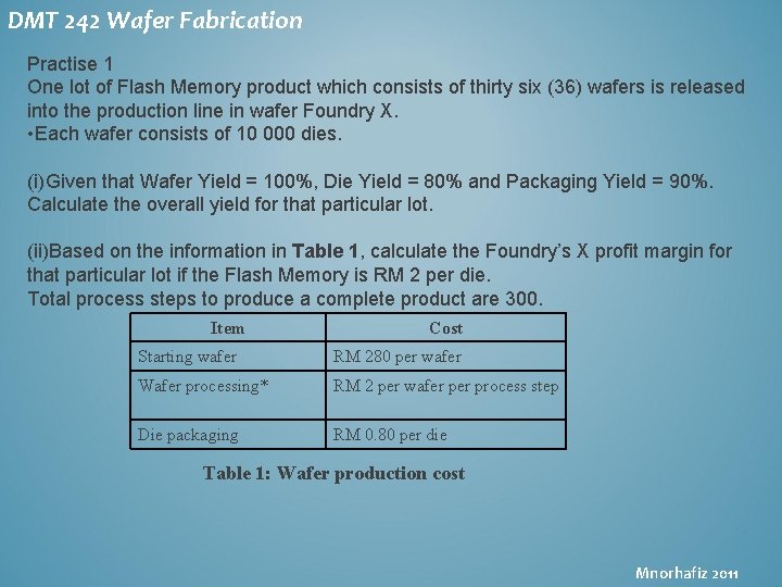
DMT 242 Wafer Fabrication Practise 1 One lot of Flash Memory product which consists of thirty six (36) wafers is released into the production line in wafer Foundry X. • Each wafer consists of 10 000 dies. (i)Given that Wafer Yield = 100%, Die Yield = 80% and Packaging Yield = 90%. Calculate the overall yield for that particular lot. (ii)Based on the information in Table 1, calculate the Foundry’s X profit margin for that particular lot if the Flash Memory is RM 2 per die. Total process steps to produce a complete product are 300. Item Cost Starting wafer RM 280 per wafer Wafer processing* RM 2 per wafer process step Die packaging RM 0. 80 per die Table 1: Wafer production cost Mnorhafiz 2011
DMT 242 Wafer Fabrication Q & A TQ Mnorhafiz 2011
- Slides: 58