DMT 234 Semiconductor Physic Device LECTURE 4 CARRIER


- Slides: 43
DMT 234 Semiconductor Physic & Device LECTURE 4 CARRIER TRANSPORT PHENOMENA
DMT 234 Semiconductor Physic & Device Preview The net flow of the electron and holes in a semiconductor will generate current. The process which these charged particles move is call transport. Two basic transport : Drift & Diffusion. The carrier transport phenomena are the foundation for finally determining the current-voltage characteristics of semiconductor devices. Subtopic : I. Carrier Drift II. Carrier Diffusion III. Hall Effect.
DMT 234 Semiconductor Physic & Device 4. 1 Carrier Drift Transport : The process which charged particles ( holes or electrons) are move. § §Understanding of the electrical properties ( I-V properties) § Basic current Equation :
DMT 234 Semiconductor Physic & Device
DMT 234 Semiconductor Physic & Device 4. 1. 1 Drift Current Density
DMT 234 Semiconductor Physic & Device 4. 1. 1 Drift Current Density
DMT 234 Semiconductor Physic & Device 4. 1. 1 Drift Current Density
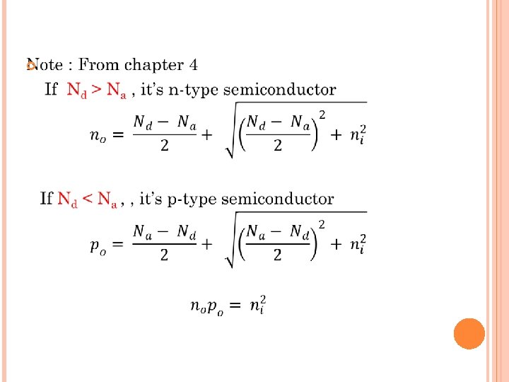
DMT 234 Semiconductor Physic & Device 4. 1. 1 Example carrier drift To calculate the drift current density in a semiconductor for a given electric field. Consider a gallium arsenide sample at T=300 K with doping concentration of Na = 0 and Nd = 1016 cm-3. Assume complete ionization and assume electron and hole mobilities given is un = 8500 cm 2/v-s and up = 400 cm 2/v-s. Calculate the drift current density if the applied electric field is E = 10 V/cm. Since Nd > Na, the semiconductor is n type and the majority carrier electron concentration: n = 10 16 cm-3 The minority carrier hole concentration is : p = n 2 i / n = (1. 8 x 10⁶)2 / 1016 = 3. 24 x 10 -4 cm-3 For this extrinsic n-type semiconductor, the drift current density is : Jdrf = e ( unn + upp)E ≈ eun. Nd. E Then , Jdrf = (1. 6 x 10 -19)(8500)(1016)(10) = 136 A/cm 2
EXERCISE A drift current density of Jdrf = 75 A/cm 2 is required in p-type silicon device when electric field of E = 120 V/cm is applied. Determine the required impurity doping concentration to achieve this specification. µn = 1350 cm 2/V. s ; µp = 480 cm 2/V. s Note : p-type s/c : Na > Nd Jdrf = e ( unn + upp)E ≈ eup. Na. E
DMT 234 Semiconductor Physic & Device 4. 1. 2 Mobility Efects
DMT 234 Semiconductor Physic & Device 4. 1. 2 Mobility Effects
DMT 234 Semiconductor Physic & Device 4. 1. 2 Mobility Effects
DMT 234 Semiconductor Physic & Device 4. 1. 2 Mobility Effects
DMT 234 Semiconductor Physic & Device 4. 1. 2 Mobility Effects
DMT 234 Semiconductor Physic & Device 4. 1. 2 Mobility Effects
DMT 234 Semiconductor Physic & Device 4. 1. 2 Mobility Effects
DMT 234 Semiconductor Physic & Device 4. 1. 2 Mobility Effects
DMT 234 Semiconductor Physic & Device 4. 1. 2 Mobility Effects
DMT 234 Semiconductor Physic & Device 4. 1. 2 Mobility Effects
DMT 234 Semiconductor Physic & Device 4. 1. 3 Conductivity
DMT 234 Semiconductor Physic & Device 4. 1. 3 Conductivity
DMT 234 Semiconductor Physic & Device 4. 1. 3 Conductivity
DMT 234 Semiconductor Physic & Device 4. 1. 3 Conductivity / resistivity
DMT 234 Semiconductor Physic & Device EXAMPLE The concentration of donor impurity atoms in silicon is Nd = 1015 cm-3. Assume an electron mobility of µn = 1300 cm 2/V. s and hole mobility, µp = 450 cm 2/V. s. i. ii. Calculate the resistivity of the material Calculate the conductivity of the material
DMT 234 Semiconductor Physic & Device 4. 1. 3 Velocity Saturation
DMT 234 Semiconductor Physic & Device 4. 2 Carrier Diffusion
DMT 234 Semiconductor Physic & Device 4. 2 Carrier Diffusion
DMT 234 Semiconductor Physic & Device 4. 2 Carrier Diffusion
DMT 234 Semiconductor Physic & Device 4. 2 Carrier Diffusion
DMT 234 Semiconductor Physic & Device 4. 2 Example Carrier Diffusion To calculate the diffusion current density given a density gradient. Assume that, in an n-type gallium arsenide semiconductor at T= 300 K, the electron concentration varies linearly from 1 x 10¹⁸ to 7 x 1017 cm-3 over a distance of 0. 10 cm. Calculate the diffusion current density if the electron diffusion coefficient is Dn = 225 cm 2/s. The diffusion current density is given : Jn|dif = e. Dn dn/dx = (1. 6 x 10 -19)(225)(1 x 10¹⁸ – 7 x 10¹⁷/0. 1) = 108 A/cm 2.
DMT 234 Semiconductor Physic & Device 4. 2 Example Carrier Diffusion To calculate the diffusion current density given a density gradient. Assume that, in an n-type gallium arsenide semiconductor at T= 300 K, the electron concentration varies linearly from 4 x 10¹⁸ to 6 x 1017 cm-3 over a distance of 0. 50 cm. Calculate the diffusion current density if the electron diffusion coefficient is Dn = 225 cm 2/s.
DMT 234 Semiconductor Physic & Device 4. 2. 1 Total current density
DMT 234 Semiconductor Physic & Device 4. 2. 1 Einstein relation
DMT 234 Semiconductor Physic & Device 4. 2. 1 Einstein relation
DMT 234 Semiconductor Physic & Device 4. 2. 1 Einstein relation
DMT 234 Semiconductor Physic & Device 4. 3 Hall Effect
DMT 234 Semiconductor Physic & Device 4. 3 Hall Effect
DMT 234 Semiconductor Physic & Device 4. 3 Hall Effect
DMT 234 Semiconductor Physic & Device 4. 3 Hall Effect
DMT 234 Semiconductor Physic & Device 4. 3 Example Hall Effect To determine the majority carrier concentration and mobility, given Hall effect parameters. Consider the geometry shown in Figure from previous slide. Let L = 10 -1 cm , W = 10 -2 cm, and d = 10 -3 cm. Also assume that Ix = 1. 0 m. A, Vx = 12. 5 V, Bz = 500 gauss = 5 x 10 -2 tesla and VH = -6. 25 m. V. A negative Hall voltage for this geometry implies that we have an n-type semiconductor using equation, we can calculate the electron concentration as : n = -(10 -3)(5 x 10 -2)/ (1. 6 x 10 -19)(10 -5)(-6. 25 x 10 -3) = 5 x 10²¹ m-3 = 5 x 1015 cm-3 The electron mobility is then determine from equation as : Un = (10 -3) / (1. 6 x 10 -19)(5 x 10²¹)(12. 5)(10 -4)(10 -5) = 0. 1 m 2/ V-s Or Un = 1000 cm 2/V-s.
DMT 234 Semiconductor Physic & Device Q & A Next week Topic : Nonequilibrium Excess Carriers in Semicondcutor.
DMT 234 Semiconductor Physic & Device