DMT 121 ELECTRONIC DEVICES CHAPTER 2 DIODE APPLICATIONS
- Slides: 40
DMT 121 ELECTRONIC DEVICES CHAPTER 2 DIODE APPLICATIONS Part 2
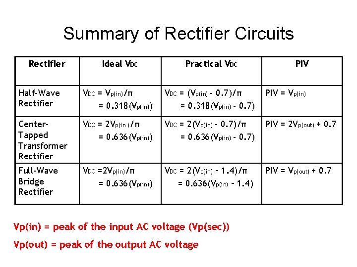
Summary of Rectifier Circuits Rectifier Ideal VDC Practical VDC Half-Wave Rectifier VDC = Vp(in)/π = 0. 318(Vp(in)) VDC = (Vp(in) - 0. 7)/π = 0. 318(Vp(in) - 0. 7) PIV = Vp(in) Center. Tapped Transformer Rectifier VDC = 2 Vp(in )/π = 0. 636(Vp(in)) VDC = 2(Vp(in) - 0. 7)/π = 0. 636(Vp(in) - 0. 7) PIV = 2 Vp(out) + 0. 7 Full-Wave Bridge Rectifier VDC =2 Vp(in)/π = 0. 636(Vp(in)) VDC = 2(Vp(in) – 1. 4)/π = 0. 636(Vp(in) – 1. 4) PIV = Vp(out) + 0. 7 Vp(in) = peak of the input AC voltage (Vp(sec)) Vp(out) = peak of the output AC voltage PIV
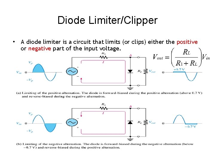
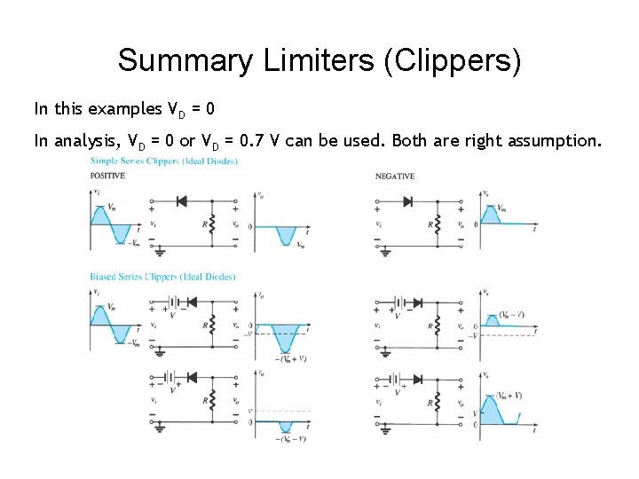
Diode Limiters (Clipper) Clippers are networks that employ diodes to “clip” away a of an input signal without distorting the remaining part of the applied waveform. Clippers used to clip-off portions of signal voltages above or below certain levels.
Diode Limiter/Clipper • A diode limiter is a circuit that limits (or clips) either the positive or negative part of the input voltage.
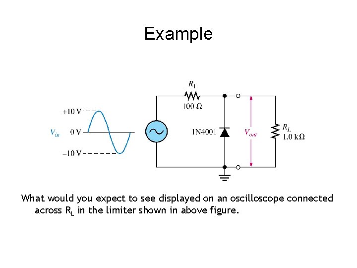
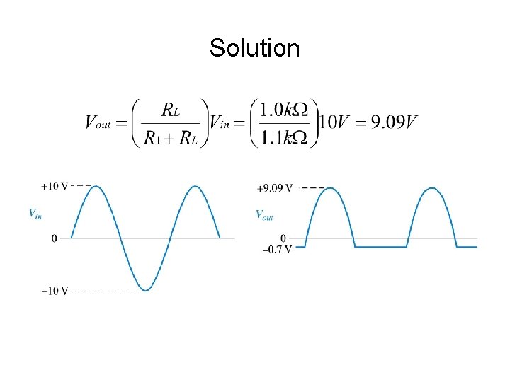
Example What would you expect to see displayed on an oscilloscope connected across RL in the limiter shown in above figure.
Solution
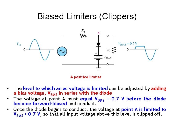
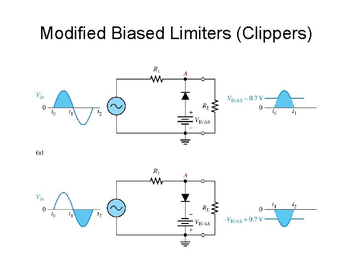
Biased Limiters (Clippers) A positive limiter • The level to which an ac voltage is limited can be adjusted by adding a bias voltage, VBIAS in series with the diode • The voltage at point A must equal VBIAS + 0. 7 V before the diode become forward-biased and conduct. • Once the diode begins to conduct, the voltage at point A is limited to VBIAS + 0. 7 V, so that all input voltage above this level is clipped off.
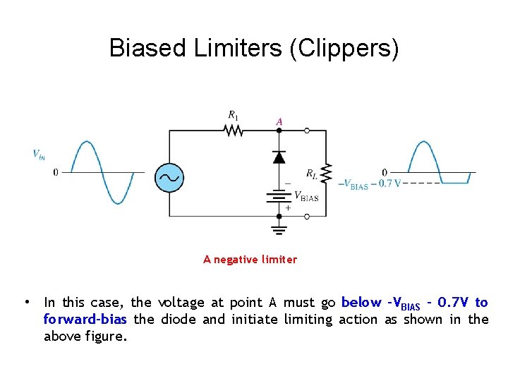
Biased Limiters (Clippers) A negative limiter • In this case, the voltage at point A must go below –VBIAS – 0. 7 V to forward-bias the diode and initiate limiting action as shown in the above figure.
Modified Biased Limiters (Clippers)
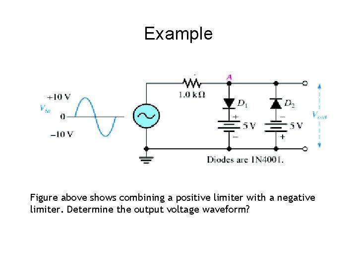
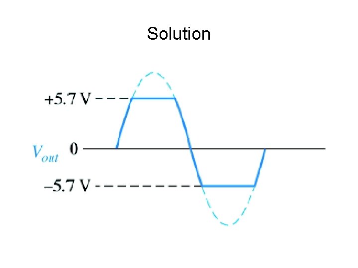
Example Figure above shows combining a positive limiter with a negative limiter. Determine the output voltage waveform?
Solution
Summary Limiters (Clippers) In this examples VD = 0 In analysis, VD = 0 or VD = 0. 7 V can be used. Both are right assumption.
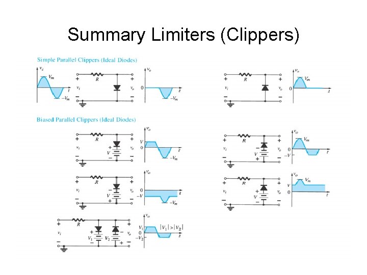
Summary Limiters (Clippers)
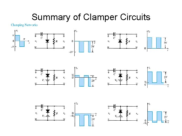
Diode Clampers • A clamper is a network constructed of a diode, a resistor, and a capacitor that shifts a waveform to a different dc level without changing the appearance of the applied signal. • Sometimes known as dc restorers • Clamping networks have a capacitor connected directly from input to output with a resistive element in parallel with the output signal. The diode is also parallel with the output signal but may or may not have a series dc supply as an added elements.
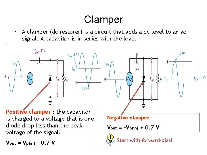
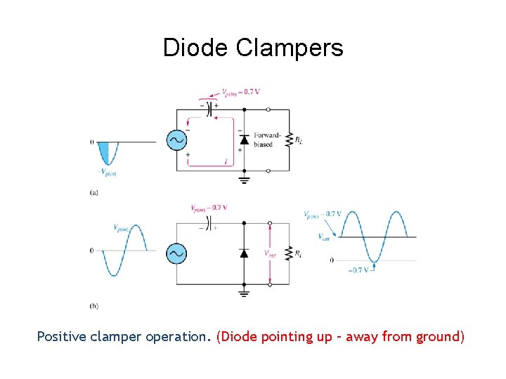
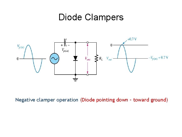
Clamper • A clamper (dc restorer) is a circuit that adds a dc level to an ac signal. A capacitor is in series with the load. Positive clamper : the capacitor is charged to a voltage that is one diode drop less than the peak voltage of the signal. Vout = Vp(in) – 0. 7 V Negative clamper Vout = -Vp(in) + 0. 7 V Start with forward-bias!
Diode Clampers Positive clamper operation. (Diode pointing up – away from ground)
Diode Clampers Negative clamper operation (Diode pointing down – toward ground)
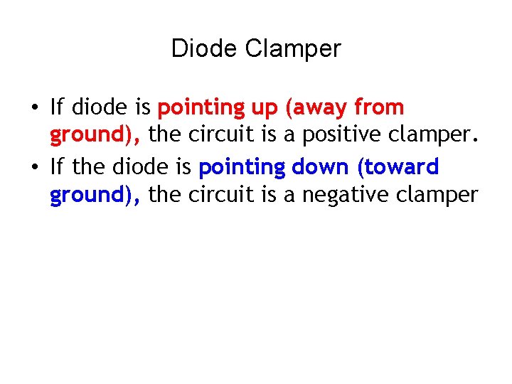
Diode Clamper • If diode is pointing up (away from ground), the circuit is a positive clamper. • If the diode is pointing down (toward ground), the circuit is a negative clamper
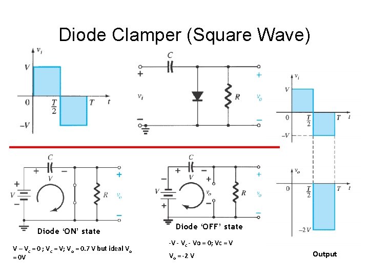
Diode Clamper (Square Wave) Diode ‘ON’ state V – Vc = 0 ; Vc = V; Vo = 0. 7 V but ideal Vo = 0 V Diode ‘OFF’ state -V - Vc - Vo = 0; Vc = V Vo = -2 V Output
Summary of Clamper Circuits
Voltage Multipliers § Voltage multiplier circuits use a combination of diodes and capacitors to step up the output voltage of rectifier circuits. • Voltage Doubler • Voltage Tripler • Voltage Quadrupler
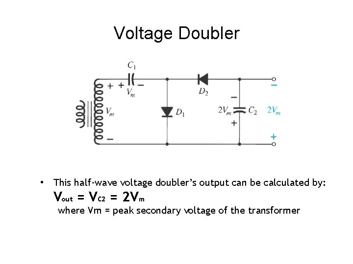
Voltage Doubler • This half-wave voltage doubler’s output can be calculated by: Vout = VC 2 = 2 Vm where Vm = peak secondary voltage of the transformer
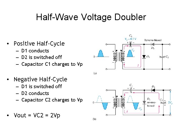
Half-Wave Voltage Doubler • Positive Half-Cycle – D 1 conducts – D 2 is switched off – Capacitor C 1 charges to Vp • Negative Half-Cycle – D 1 is switched off – D 2 conducts – Capacitor C 2 charges to Vp • Vout = VC 2 = 2 Vp
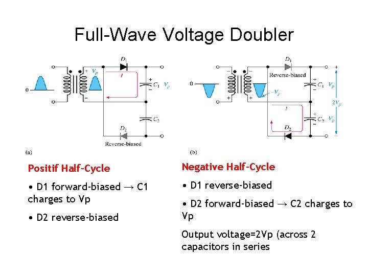
Full-Wave Voltage Doubler Positif Half-Cycle Negative Half-Cycle • D 1 forward-biased → C 1 charges to Vp • D 1 reverse-biased • D 2 forward-biased → C 2 charges to Vp Output voltage=2 Vp (across 2 capacitors in series
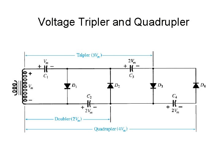
Voltage Tripler and Quadrupler
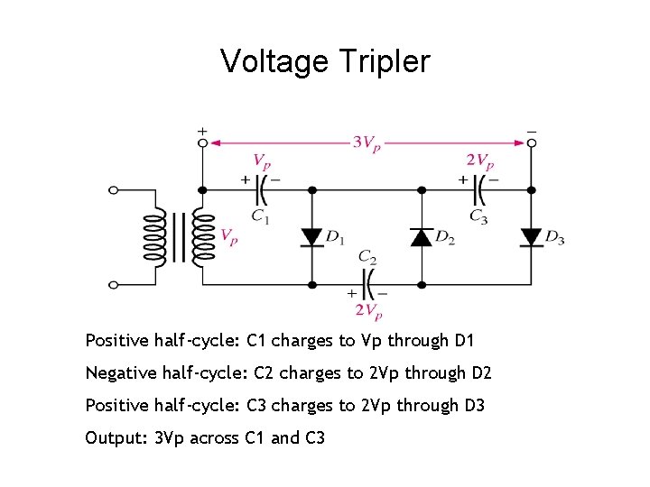
Voltage Tripler Positive half-cycle: C 1 charges to Vp through D 1 Negative half-cycle: C 2 charges to 2 Vp through D 2 Positive half-cycle: C 3 charges to 2 Vp through D 3 Output: 3 Vp across C 1 and C 3
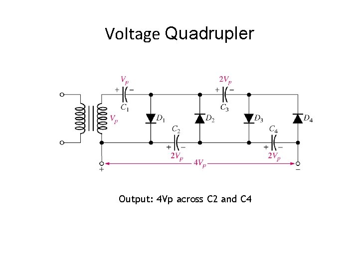
Voltage Quadrupler Output: 4 Vp across C 2 and C 4
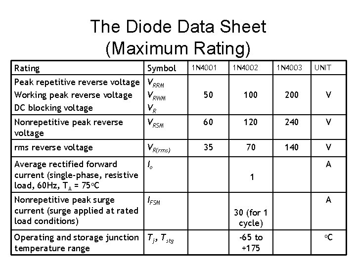
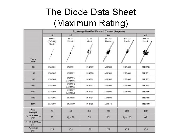
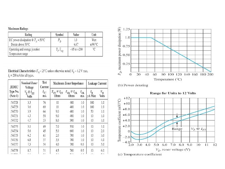
The Diode Data Sheet The data sheet for diodes and other devices gives detailed information about specific characteristics such as the various maximum current and voltage ratings, temperature range, and voltage versus current curves (V-I characteristic). • It is sometimes a very valuable piece of information, even for a technician. There are cases when you might have to select a replacement diode when the type of diode needed may no longer be available. • These are the absolute max. values under which the diode can be operated without damage to the device. •
The Diode Data Sheet (Maximum Rating) Rating Symbol Peak repetitive reverse voltage VRRM Working peak reverse voltage VRWM DC blocking voltage VR 1 N 4001 1 N 4002 1 N 4003 UNIT 50 100 200 V Nonrepetitive peak reverse voltage VRSM 60 120 240 V rms reverse voltage VR(rms) 35 70 140 V Average rectified forward current (single-phase, resistive load, 60 Hz, TA = 75 o. C Io Nonrepetitive peak surge current (surge applied at rated load conditions) IFSM A 1 Operating and storage junction Tj, Tstg temperature range A 30 (for 1 cycle) -65 to +175 o. C
The Diode Data Sheet (Maximum Rating)
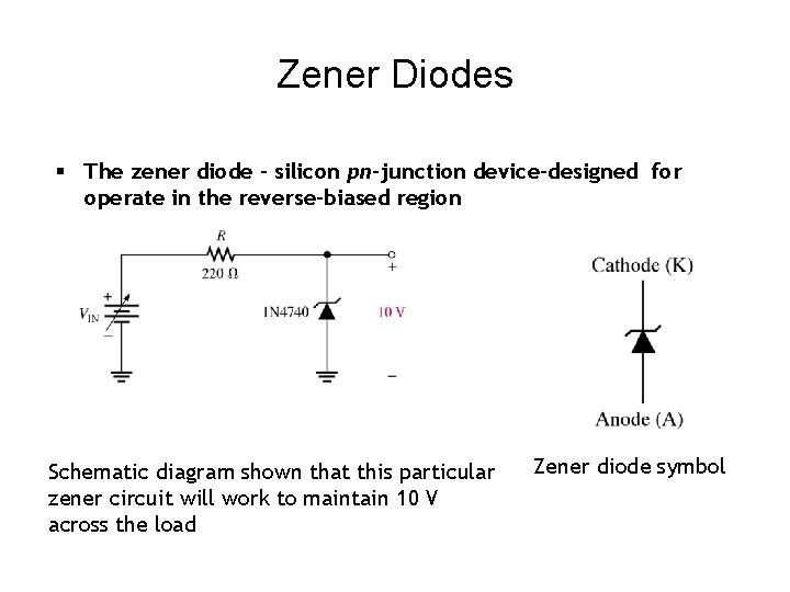
Zener Diodes § The zener diode – silicon pn-junction device-designed for operate in the reverse-biased region Schematic diagram shown that this particular zener circuit will work to maintain 10 V across the load Zener diode symbol
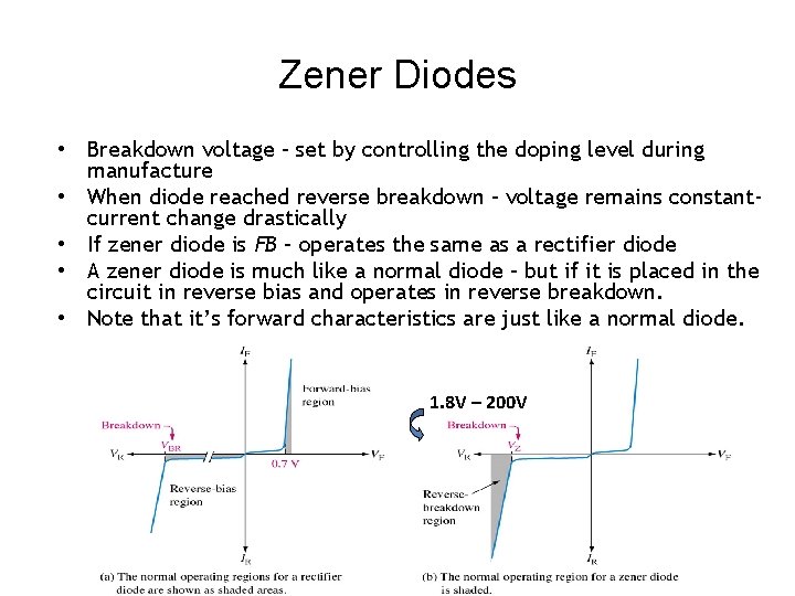
Zener Diodes • Breakdown voltage – set by controlling the doping level during manufacture • When diode reached reverse breakdown – voltage remains constantcurrent change drastically • If zener diode is FB – operates the same as a rectifier diode • A zener diode is much like a normal diode – but if it is placed in the circuit in reverse bias and operates in reverse breakdown. • Note that it’s forward characteristics are just like a normal diode. 1. 8 V – 200 V
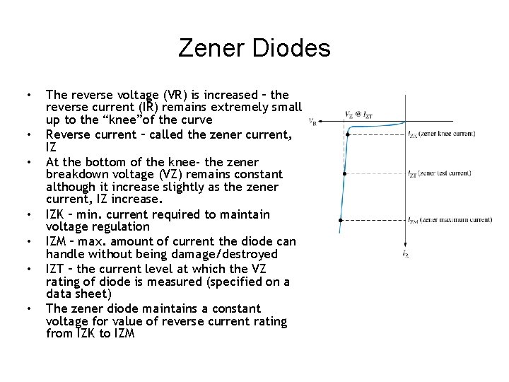
Zener Diodes • • The reverse voltage (VR) is increased – the reverse current (IR) remains extremely small up to the “knee”of the curve Reverse current – called the zener current, IZ At the bottom of the knee- the zener breakdown voltage (VZ) remains constant although it increase slightly as the zener current, IZ increase. IZK – min. current required to maintain voltage regulation IZM – max. amount of current the diode can handle without being damage/destroyed IZT – the current level at which the VZ rating of diode is measured (specified on a data sheet) The zener diode maintains a constant voltage for value of reverse current rating from IZK to IZM
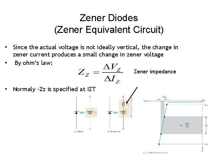
Zener Diodes (Zener Equivalent Circuit) • Since the actual voltage is not ideally vertical, the change in zener current produces a small change in zener voltage • By ohm’s law: Zener impedance • Normaly -Zz is specified at IZT
Zener Diodes (Temp Coeff & Zener Power Dissipation and Derating) • As with most devices, zener diodes have given characteristics such as temperature coefficients and power ratings that have to be considered. The data sheet provides this information
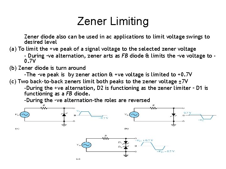
Zener Diodes Applications • Zener diode can be used as 1. Voltage regulator for providing stable reference voltages 2. Simple limiters or clippers
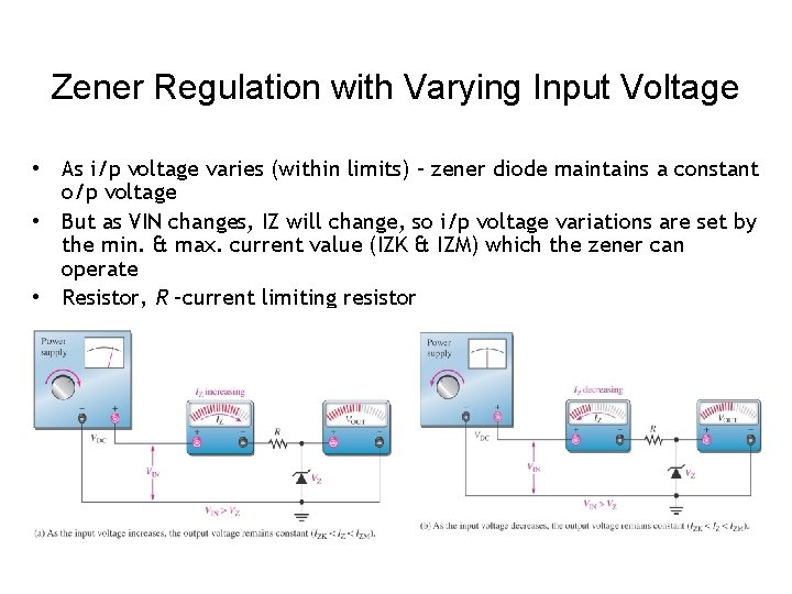
Zener Regulation with Varying Input Voltage • As i/p voltage varies (within limits) – zener diode maintains a constant o/p voltage • But as VIN changes, IZ will change, so i/p voltage variations are set by the min. & max. current value (IZK & IZM) which the zener can operate • Resistor, R –current limiting resistor
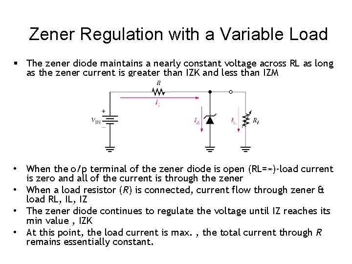
Zener Regulation with a Variable Load § The zener diode maintains a nearly constant voltage across RL as long as the zener current is greater than IZK and less than IZM • When the o/p terminal of the zener diode is open (RL=∞)-load current is zero and all of the current is through the zener • When a load resistor (R) is connected, current flow through zener & load RL, IZ • The zener diode continues to regulate the voltage until IZ reaches its min value , IZK • At this point, the load current is max. , the total current through R remains essentially constant.
Zener Limiting Zener diode also can be used in ac applications to limit voltage swings to desired level (a) To limit the +ve peak of a signal voltage to the selected zener voltage - During –ve alternation, zener arts as FB diode & limits the –ve voltage to 0. 7 V (b) Zener diode is turn around -The –ve peak is by zener action & +ve voltage is limited to +0. 7 V (c) Two back-to-back zeners limit both peaks to the zener voltage ± 7 V -During the +ve alternation, D 2 is functioning as the zener limiter – D 1 is functioning as a FB diode. -During the –ve alternation-the roles are reversed