
DMT 121 ELECTRONIC DEVICES CHAPTER 5 FIELDEFFECT TRANSISTOR
- Slides: 27
DMT 121 – ELECTRONIC DEVICES CHAPTER 5 FIELD-EFFECT TRANSISTOR (FET) -MOSFET-
MOSFET ¡ ¡ MOSFET (Metal Oxide Semiconductor Field-Effect Transistor) Different from JFET – no pn junction structure. Gate of MOSFET is insulated from the channel by silicon dioxide (Si. O 2) layer. 2 types – enhancement and depletion.
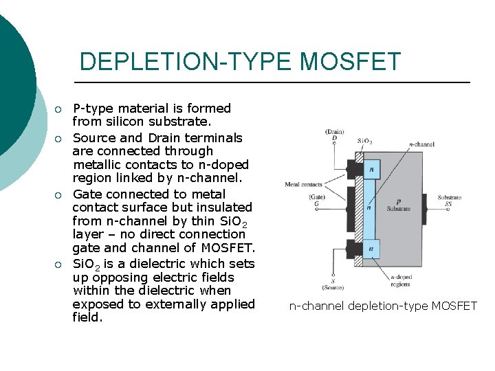
DEPLETION-TYPE MOSFET ¡ ¡ P-type material is formed from silicon substrate. Source and Drain terminals are connected through metallic contacts to n-doped region linked by n-channel. Gate connected to metal contact surface but insulated from n-channel by thin Si. O 2 layer – no direct connection gate and channel of MOSFET. Si. O 2 is a dielectric which sets up opposing electric fields within the dielectric when exposed to externally applied field. n-channel depletion-type MOSFET
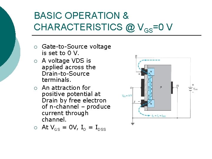
BASIC OPERATION & CHARACTERISTICS @ VGS=0 V ¡ ¡ Gate-to-Source voltage is set to 0 V. A voltage VDS is applied across the Drain-to-Source terminals. An attraction for positive potential at Drain by free electron of n-channel – produce current through channel. At VGS = 0 V, ID = IDSS
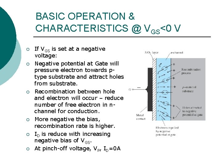
BASIC OPERATION & CHARACTERISTICS @ VGS<0 V ¡ ¡ ¡ If VGS is set at a negative voltage: Negative potential at Gate will pressure electron towards ptype substrate and attract holes from substrate. Recombination between hole and electron will occur – reduce number of free electron in nchannel for conduction. More negative the bias, recombination rate is higher. ID is reduce with increasing negative bias of VGS. At pinch-off voltage, VP, ID=0 A
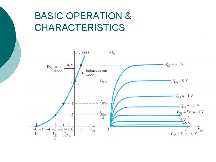
BASIC OPERATION & CHARACTERISTICS @ VGS>0 V ¡ ¡ ¡ For positive value of VGS: Positive Gate will draw additional electron from psubstrate due to reverse leakage current and established new carrier through the collisions between accelerating particles. ID will increase at rapid rate – user must aware of I D maximum current rating. Application of positive VGS has enhance the level of free carriers in the channel. Region of positive gate voltage on drain or transfer curve is called enhancement region while region between saturation and cutoff is called depletion region.
BASIC OPERATION & CHARACTERISTICS
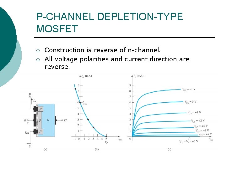
P-CHANNEL DEPLETION-TYPE MOSFET ¡ ¡ Construction is reverse of n-channel. All voltage polarities and current direction are reverse.
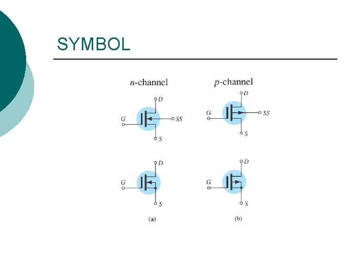
SYMBOL
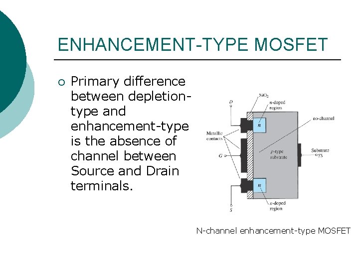
ENHANCEMENT-TYPE MOSFET ¡ Primary difference between depletiontype and enhancement-type is the absence of channel between Source and Drain terminals. N-channel enhancement-type MOSFET
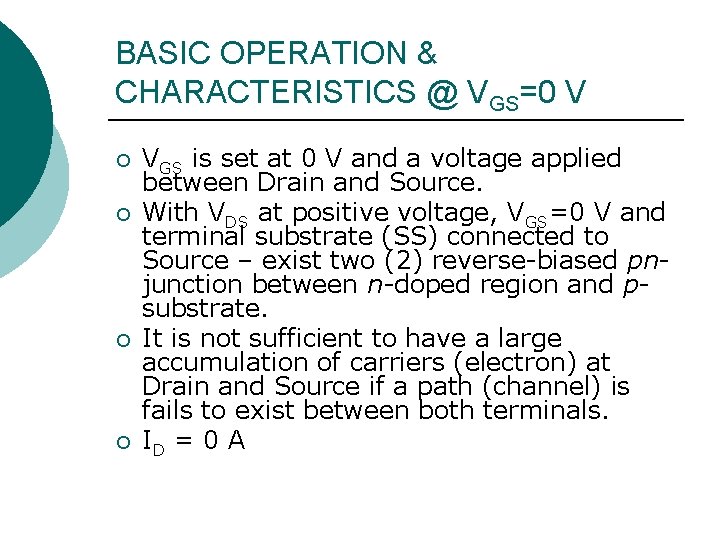
BASIC OPERATION & CHARACTERISTICS @ VGS=0 V ¡ ¡ VGS is set at 0 V and a voltage applied between Drain and Source. With VDS at positive voltage, VGS=0 V and terminal substrate (SS) connected to Source – exist two (2) reverse-biased pnjunction between n-doped region and psubstrate. It is not sufficient to have a large accumulation of carriers (electron) at Drain and Source if a path (channel) is fails to exist between both terminals. ID = 0 A
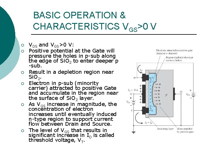
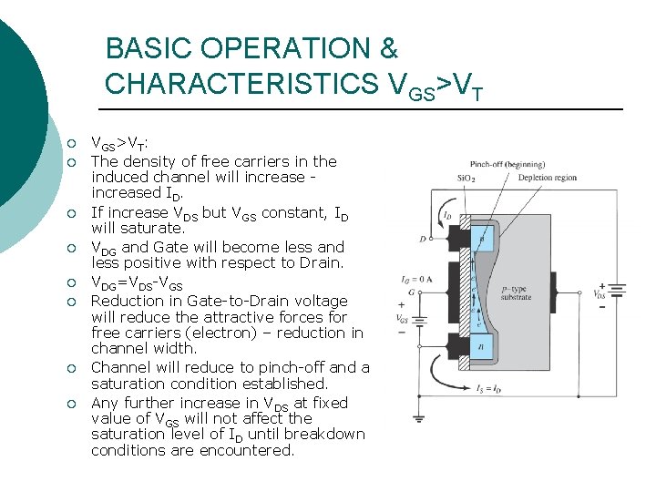
BASIC OPERATION & CHARACTERISTICS VGS>0 V ¡ ¡ ¡ VDS and VGS>0 V: Positive potential at the Gate will pressure the holes in p-sub along the edge of Si. O 2 to enter deeper p -sub. Result in a depletion region near Si. O 2. Electron in p-sub (minority carrier) attracted to positive Gate and accumulate in the region near the surface of Si. O 2 layer. As VGS increase in magnitude, the concentration of electron increases until eventually induced n-type region to support current flow between Drain and Source. The level of VGS that results in significant increase in ID is called threshold voltage, VT.
BASIC OPERATION & CHARACTERISTICS VGS>VT ¡ ¡ ¡ ¡ VGS>VT: The density of free carriers in the induced channel will increased ID. If increase VDS but VGS constant, ID will saturate. VDG and Gate will become less and less positive with respect to Drain. VDG=VDS-VGS Reduction in Gate-to-Drain voltage will reduce the attractive forces for free carriers (electron) – reduction in channel width. Channel will reduce to pinch-off and a saturation condition established. Any further increase in VDS at fixed value of VGS will not affect the saturation level of ID until breakdown conditions are encountered.
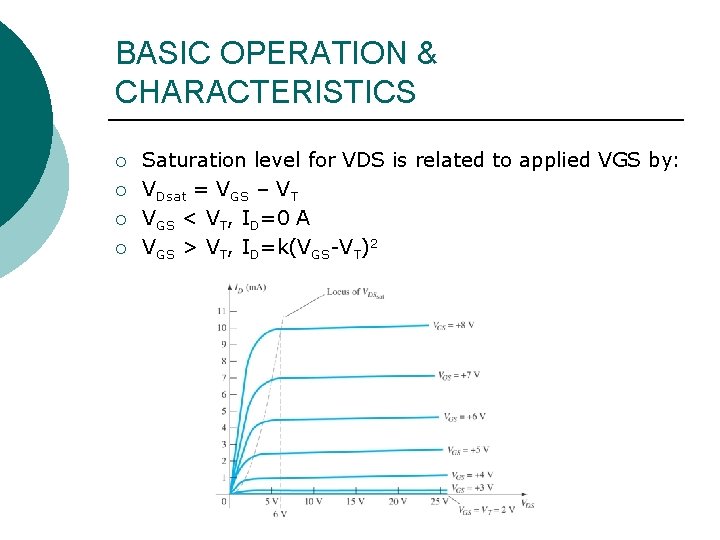
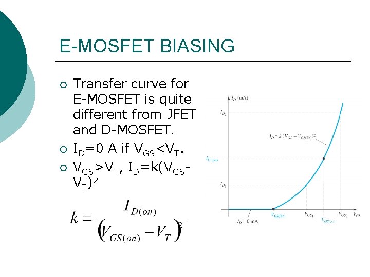
BASIC OPERATION & CHARACTERISTICS ¡ ¡ Saturation level for VDS is related to applied VGS by: VDsat = VGS – VT VGS < VT, ID=0 A VGS > VT, ID=k(VGS-VT)2
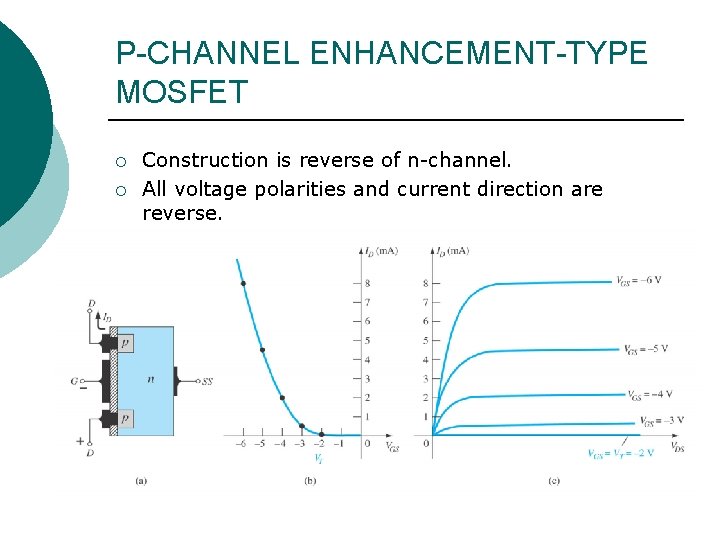
P-CHANNEL ENHANCEMENT-TYPE MOSFET ¡ ¡ Construction is reverse of n-channel. All voltage polarities and current direction are reverse.
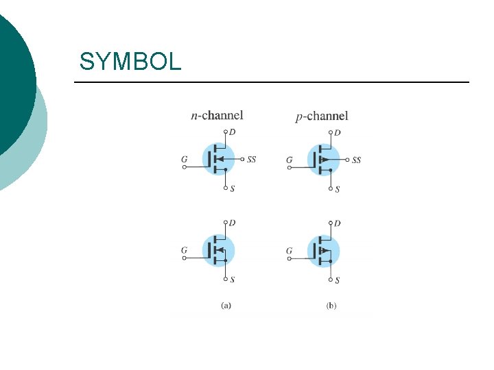
SYMBOL
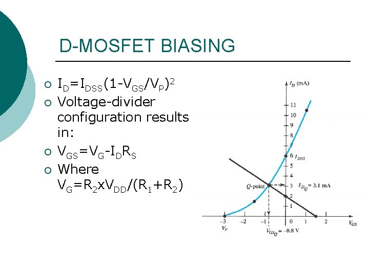
D-MOSFET BIASING ¡ ¡ Similarities in appearance between transfer curve of JFET and D-MOSFET. Primary difference: D-MOSFET permit operating points with positive value of VGS and level of ID that exceed IDSS.
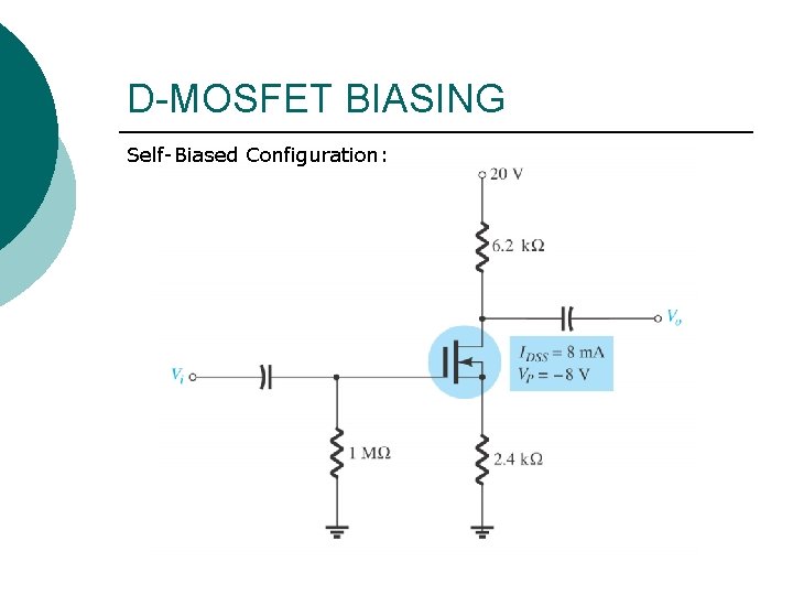
D-MOSFET BIASING Self-Biased Configuration:
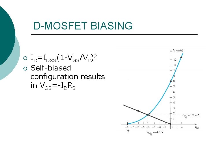
D-MOSFET BIASING ¡ ¡ ID=IDSS(1 -VGS/VP)2 Self-biased configuration results in VGS=-IDRS
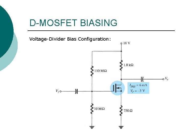
D-MOSFET BIASING Voltage-Divider Bias Configuration:
D-MOSFET BIASING ¡ ¡ ID=IDSS(1 -VGS/VP)2 Voltage-divider configuration results in: VGS=VG-IDRS Where VG=R 2 x. VDD/(R 1+R 2)
E-MOSFET BIASING ¡ ¡ ¡ Transfer curve for E-MOSFET is quite different from JFET and D-MOSFET. ID=0 A if VGS<VT. VGS>VT, ID=k(VGSV T )2
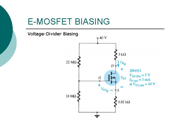
E-MOSFET BIASING Voltage-Divider Biasing
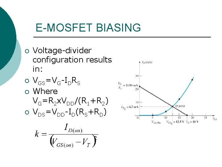
E-MOSFET BIASING ¡ ¡ Voltage-divider configuration results in: VGS=VG-IDRS Where VG=R 2 x. VDD/(R 1+R 2) VDS=VDD-ID(RS+RD)
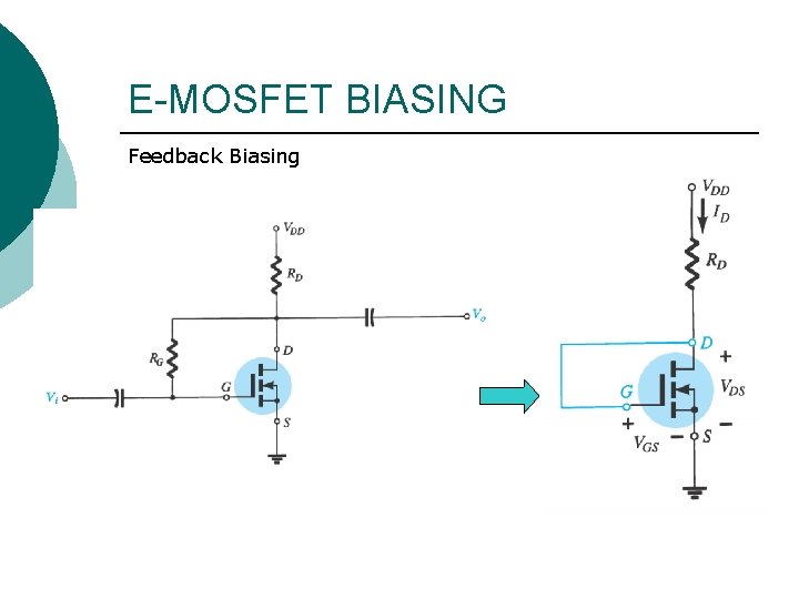
E-MOSFET BIASING Feedback Biasing
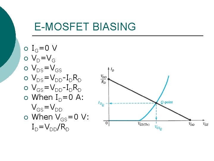
E-MOSFET BIASING ¡ ¡ ¡ ¡ IG=0 V VD=VG VDS=VGS VDS=VDD-IDRD VGS=VDD-IDRD When ID=0 A: VGS=VDD When VGS=0 V: ID=VDD/RD
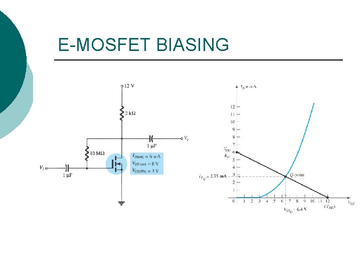
E-MOSFET BIASING