Design of Digital Circuits Lecture 8 Timing and








- Slides: 98

Design of Digital Circuits Lecture 8: Timing and Verification Minesh Patel Prof. Onur Mutlu ETH Zurich Spring 2018 16 March 2018

Readings n Please study Slides 102 -120 from Lecture 6 on your own n This week q Sequential Logic n q H&H Chapter 4 in full Timing and Verification n n H&H Chapter 3 in full Hardware Description Languages and Verilog n q P&P Chapter 3. 4 until end + H&H Chapters 2. 9 and 3. 5 + Chapter 5 Next week q Von Neumann Model, LC 3, and MIPS n q P&P Chapter 4 -5 + H&H Chapter 6 Digital Building Blocks n H&H Chapter 5 2

What Will We Learn Today? n Timing in combinational circuits q q n Timing in sequential circuits q q n Propagation delay and contamination delay Glitches Setup time and hold time Determining how fast a circuit can operate Circuit Verification q q q How to make sure a circuit works correctly Functional verification Timing verification 3

Tradeoffs in Circuit Design 4

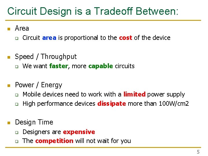
Circuit Design is a Tradeoff Between: n Area q n Speed / Throughput q n We want faster, more capable circuits Power / Energy q q n Circuit area is proportional to the cost of the device Mobile devices need to work with a limited power supply High performance devices dissipate more than 100 W/cm 2 Design Time q q Designers are expensive The competition will not wait for you 5

Requirements and Goals Depend On Application 6

Circuit Timing n Until now, we investigated logical functionality n What about timing? q q q n How fast is a circuit? How can we make a circuit faster? What happens if we run a circuit too fast? A design that is logically correct can still fail because of real -world implementation issues! 7

Part 1: Combinational Circuit Timing 8

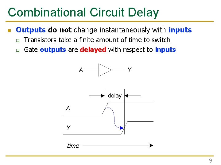
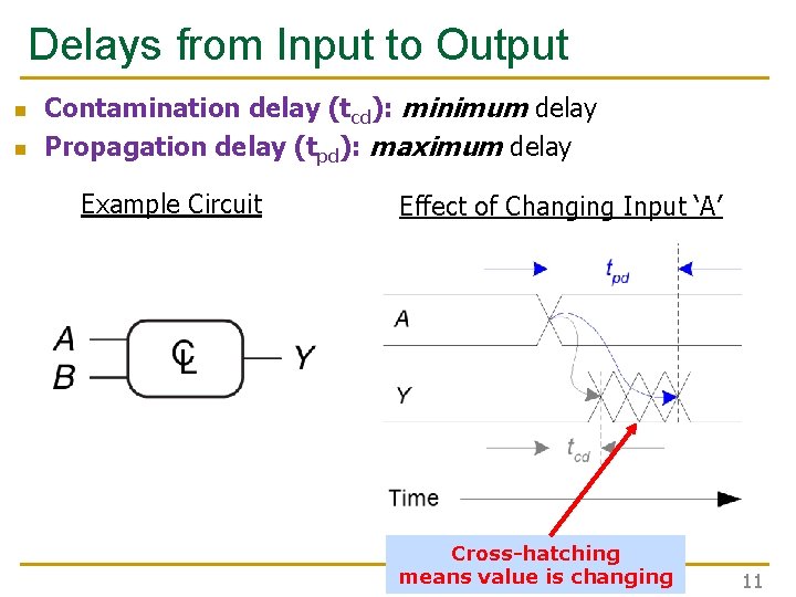
Combinational Circuit Delay n Outputs do not change instantaneously with inputs q q Transistors take a finite amount of time to switch Gate outputs are delayed with respect to inputs time 9

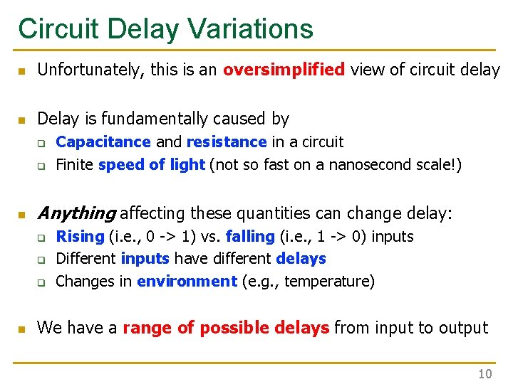
Circuit Delay Variations n Unfortunately, this is an oversimplified view of circuit delay n Delay is fundamentally caused by q q n Anything affecting these quantities can change delay: q q q n Capacitance and resistance in a circuit Finite speed of light (not so fast on a nanosecond scale!) Rising (i. e. , 0 -> 1) vs. falling (i. e. , 1 -> 0) inputs Different inputs have different delays Changes in environment (e. g. , temperature) We have a range of possible delays from input to output 10

Delays from Input to Output n n Contamination delay (tcd): minimum delay Propagation delay (tpd): maximum delay Example Circuit Effect of Changing Input ‘A’ Cross-hatching means value is changing 11

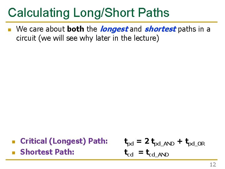
Calculating Long/Short Paths We care about both the longest and shortest paths in a circuit (we will see why later in the lecture) n n n Critical (Longest) Path: Shortest Path: tpd = 2 tpd_AND + tpd_OR tcd = tcd_AND 12

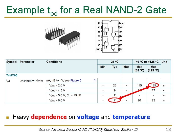
Example tpd for a Real NAND-2 Gate n Heavy dependence on voltage and temperature! Source: Nexperia 2 -input NAND (74 HC 00) Datasheet, Section 10 13

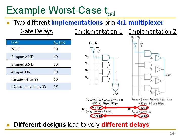
Example Worst-Case tpd n n Two different implementations of a 4: 1 multiplexer Gate Delays Implementation 1 Implementation 2 Different designs lead to very different delays 14

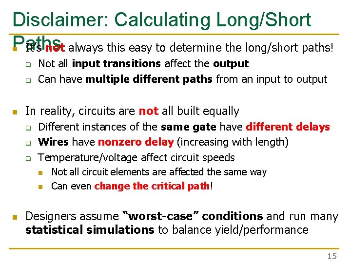
Disclaimer: Calculating Long/Short Paths n It’s not always this easy to determine the long/short paths! q q n Not all input transitions affect the output Can have multiple different paths from an input to output In reality, circuits are not all built equally q q q Different instances of the same gate have different delays Wires have nonzero delay (increasing with length) Temperature/voltage affect circuit speeds n n n Not all circuit elements are affected the same way Can even change the critical path! Designers assume “worst-case” conditions and run many statistical simulations to balance yield/performance 15

Combinational Timing Summary n Circuit outputs change some time after the inputs change q q n n Caused by finite speed of light (not so fast on a ns scale!) Delay is dependent on inputs, environmental state, etc. The range of possible delays is characterized by: q Contamination delay (tcd): minimum possible delay q Propagation delay (tpd): maximum possible delay Different circuit topologies can have different delays 16

Output Glitches 17

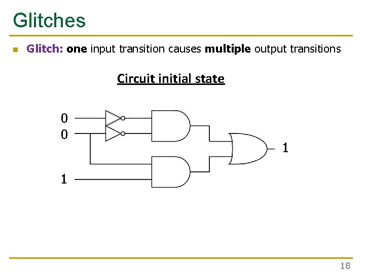
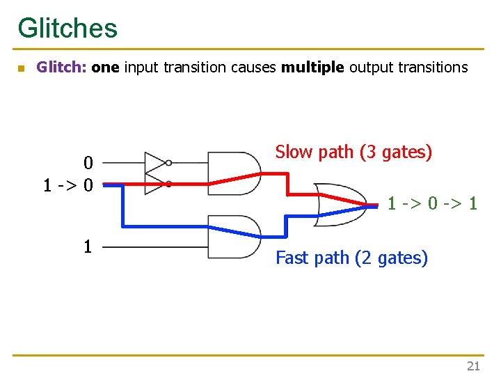
Glitches n Glitch: one input transition causes multiple output transitions Circuit initial state 0 0 1 1 18

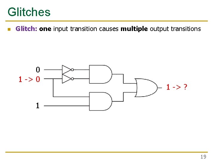
Glitches n Glitch: one input transition causes multiple output transitions 0 1 -> ? 1 19

Glitches n Glitch: one input transition causes multiple output transitions 0 1 -> 0 1 Slow path (3 gates) 1 -> ? Fast path (2 gates) 20

Glitches n Glitch: one input transition causes multiple output transitions 0 1 -> 0 1 Slow path (3 gates) 1 -> 0 -> 1 Fast path (2 gates) 21

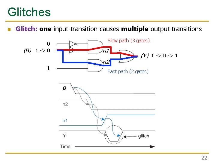
Glitches n Glitch: one input transition causes multiple output transitions 0 (B) 1 -> 0 Slow path (3 gates) n 1 (Y) 1 -> 0 -> 1 n 2 1 Fast path (2 gates) 22

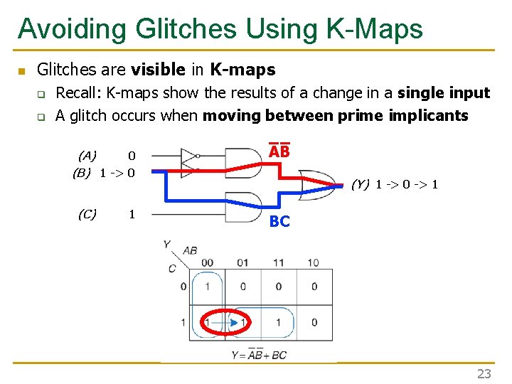
Avoiding Glitches Using K-Maps n Glitches are visible in K-maps q q Recall: K-maps show the results of a change in a single input A glitch occurs when moving between prime implicants (A) 0 (B) 1 -> 0 (C) 1 AB (Y) 1 -> 0 -> 1 BC 23

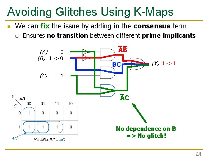
Avoiding Glitches Using K-Maps n We can fix the issue by adding in the consensus term q Ensures no transition between different prime implicants (A) 0 (B) 1 -> 0 (C) AB BC (Y) 1 -> 1 1 AC No dependence on B => No glitch! 24

Avoiding Glitches n Q: Do we always care about glitches? q Fixing glitches is undesirable n n n q n More chip area More power consumption More design effort The circuit is eventually guaranteed to converge to the right value regardless of glitchiness A: No, not always! q q If we only care about the long-term steady state output, we can safely ignore glitches Up to the designer to decide if glitches matter in their application 25

Part 2: Sequential Circuit Timing 26

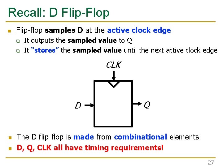
Recall: D Flip-Flop n Flip-flop samples D at the active clock edge q q It outputs the sampled value to Q It “stores” the sampled value until the next active clock edge CLK D n n Q The D flip-flop is made from combinational elements D, Q, CLK all have timing requirements! 27

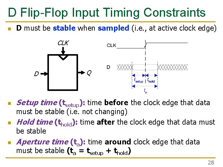
D Flip-Flop Input Timing Constraints n D must be stable when sampled (i. e. , at active clock edge) CLK D n n n Q Setup time (tsetup): time before the clock edge that data must be stable (i. e. not changing) Hold time (thold): time after the clock edge that data must be stable Aperture time (ta): time around clock edge that data must be stable (ta = tsetup + thold) 28

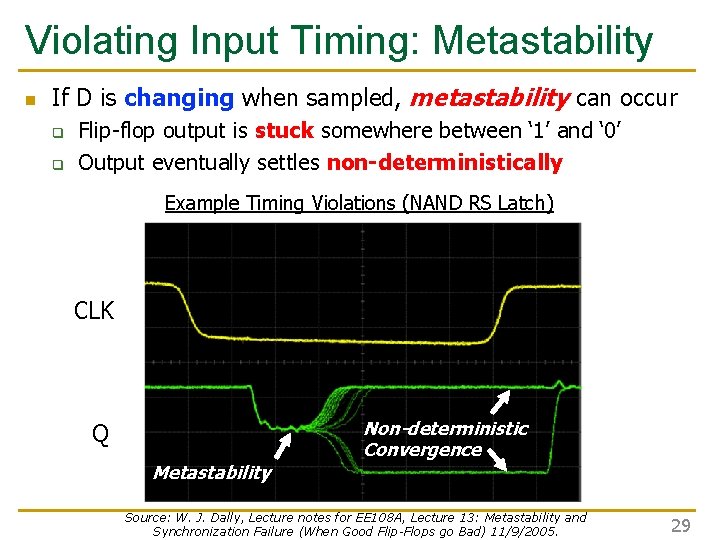
Violating Input Timing: Metastability n If D is changing when sampled, metastability can occur q q Flip-flop output is stuck somewhere between ‘ 1’ and ‘ 0’ Output eventually settles non-deterministically Example Timing Violations (NAND RS Latch) CLK Non-deterministic Convergence Q Metastability Source: W. J. Dally, Lecture notes for EE 108 A, Lecture 13: Metastability and Synchronization Failure (When Good Flip-Flops go Bad) 11/9/2005. 29

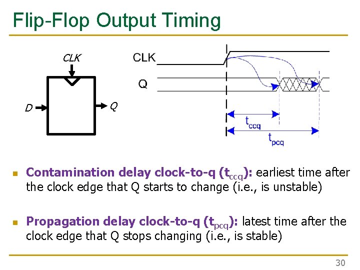
Flip-Flop Output Timing CLK D n n Q Contamination delay clock-to-q (tccq): earliest time after the clock edge that Q starts to change (i. e. , is unstable) Propagation delay clock-to-q (tpcq): latest time after the clock edge that Q stops changing (i. e. , is stable) 30

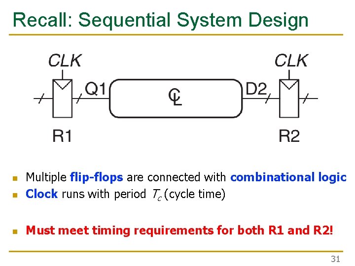
Recall: Sequential System Design n Multiple flip-flops are connected with combinational logic Clock runs with period Tc (cycle time) n Must meet timing requirements for both R 1 and R 2! n 31

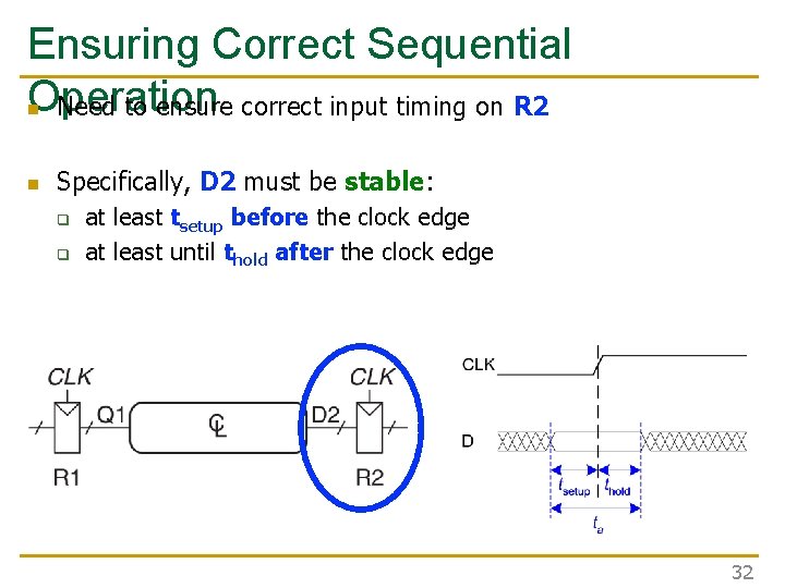
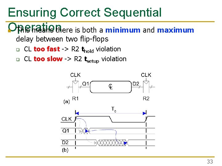
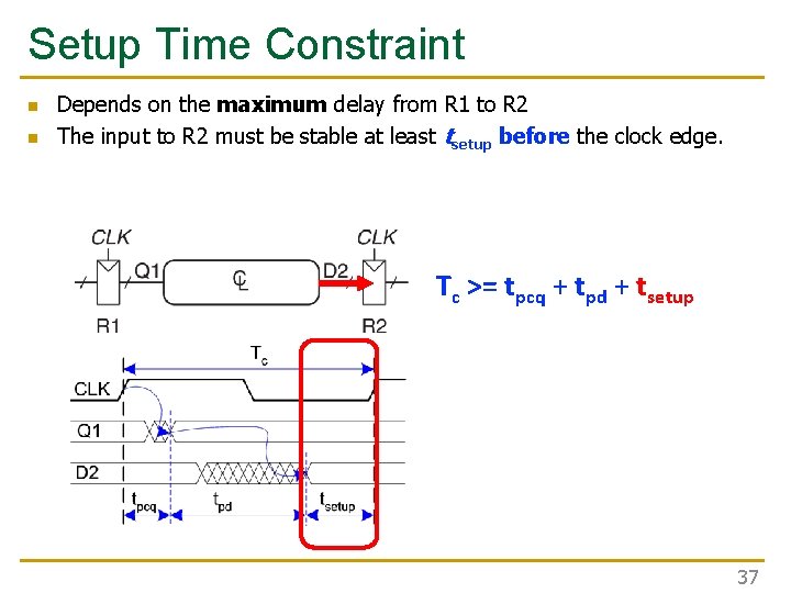
Ensuring Correct Sequential Operation n Need to ensure correct input timing on R 2 n Specifically, D 2 must be stable: q q at least tsetup before the clock edge at least until thold after the clock edge 32

Ensuring Correct Sequential Operation n This means there is both a minimum and maximum delay between two flip-flops q q CL too fast -> R 2 thold violation CL too slow -> R 2 tsetup violation 33

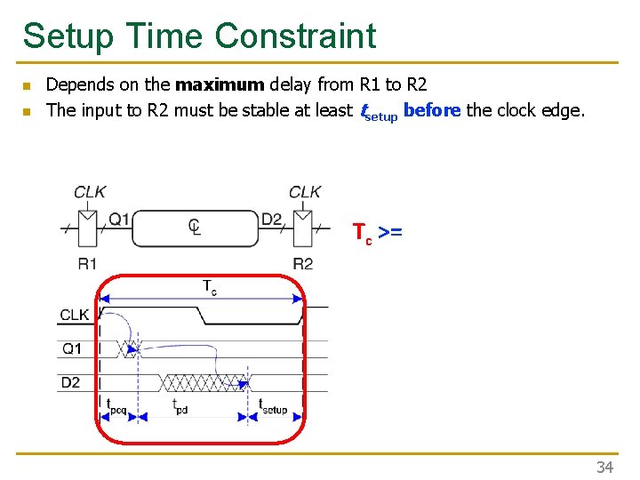
Setup Time Constraint n n Depends on the maximum delay from R 1 to R 2 The input to R 2 must be stable at least tsetup before the clock edge. Tc >= 34

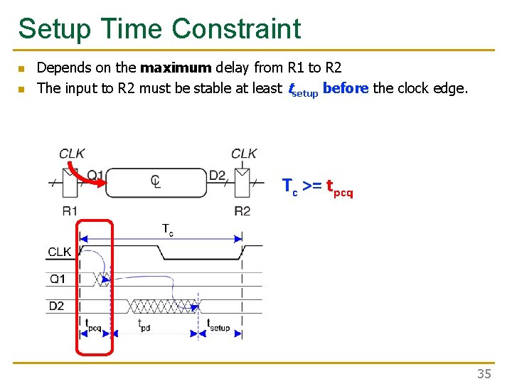
Setup Time Constraint n n Depends on the maximum delay from R 1 to R 2 The input to R 2 must be stable at least tsetup before the clock edge. Tc >= tpcq 35

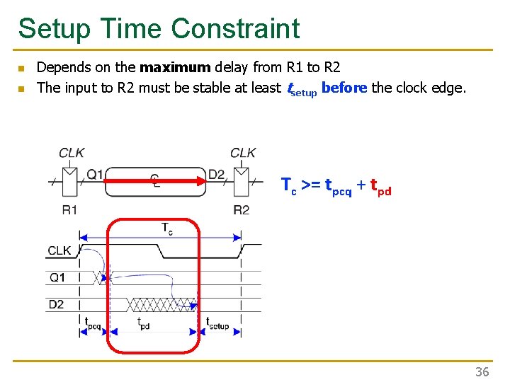
Setup Time Constraint n n Depends on the maximum delay from R 1 to R 2 The input to R 2 must be stable at least tsetup before the clock edge. Tc >= tpcq + tpd 36

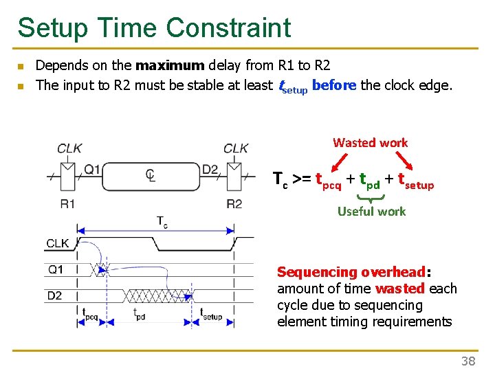
Setup Time Constraint n n Depends on the maximum delay from R 1 to R 2 The input to R 2 must be stable at least tsetup before the clock edge. Tc >= tpcq + tpd + tsetup 37

Setup Time Constraint n n Depends on the maximum delay from R 1 to R 2 The input to R 2 must be stable at least tsetup before the clock edge. Wasted work Tc >= tpcq + tpd + tsetup Useful work Sequencing overhead: amount of time wasted each cycle due to sequencing element timing requirements 38

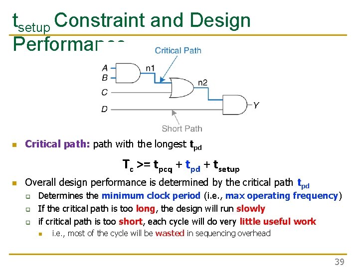
tsetup Constraint and Design Performance n Critical path: path with the longest tpd Tc >= tpcq + tpd + tsetup n Overall design performance is determined by the critical path tpd q q q Determines the minimum clock period (i. e. , max operating frequency) If the critical path is too long, the design will run slowly if critical path is too short, each cycle will do very little useful work n i. e. , most of the cycle will be wasted in sequencing overhead 39

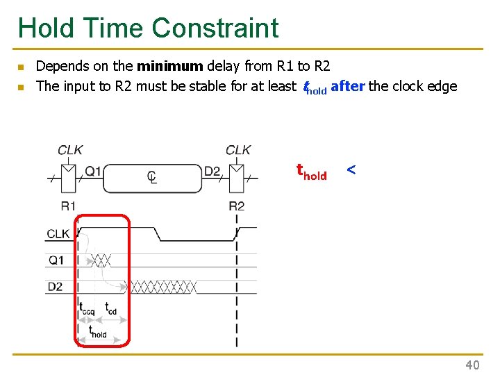
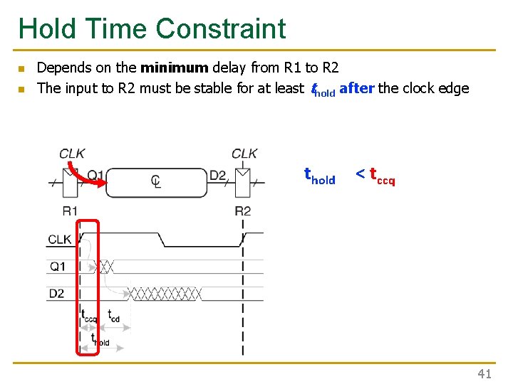
Hold Time Constraint n n Depends on the minimum delay from R 1 to R 2 The input to R 2 must be stable for at least thold after the clock edge thold < 40

Hold Time Constraint n n Depends on the minimum delay from R 1 to R 2 The input to R 2 must be stable for at least thold after the clock edge thold < tccq 41

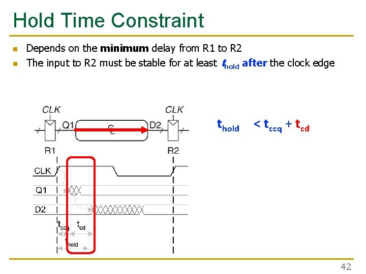
Hold Time Constraint n n Depends on the minimum delay from R 1 to R 2 The input to R 2 must be stable for at least thold after the clock edge thold < tccq + tcd 42

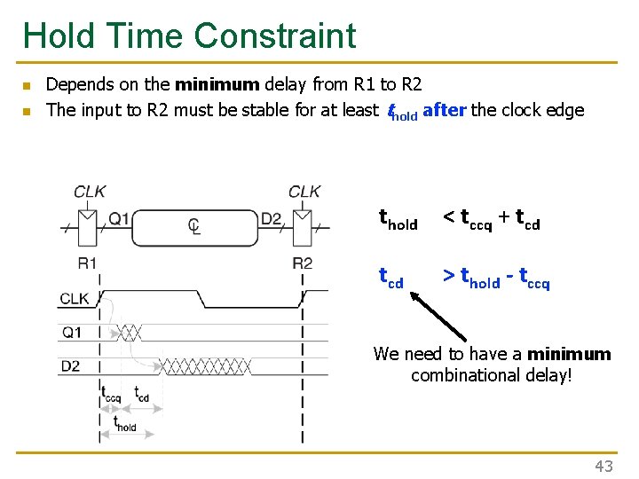
Hold Time Constraint n n Depends on the minimum delay from R 1 to R 2 The input to R 2 must be stable for at least thold after the clock edge thold < tccq + tcd > thold - tccq We need to have a minimum combinational delay! 43

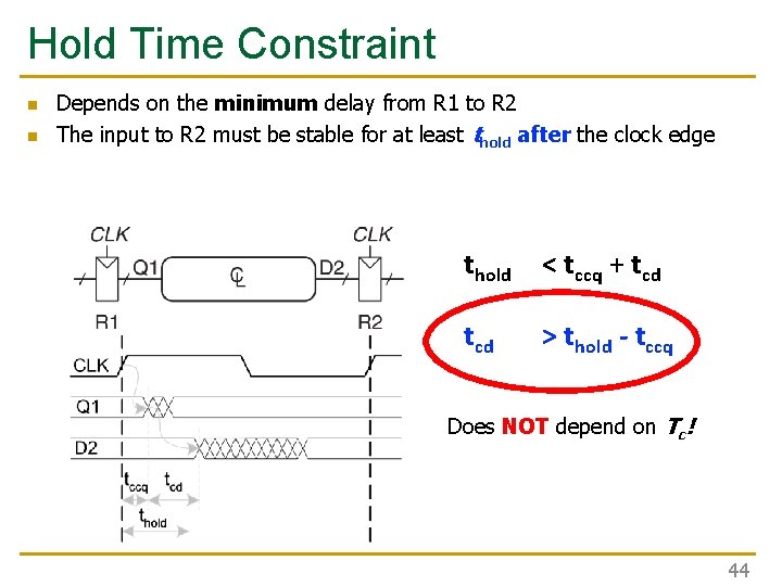
Hold Time Constraint n n Depends on the minimum delay from R 1 to R 2 The input to R 2 must be stable for at least thold after the clock edge thold < tccq + tcd > thold - tccq Does NOT depend on Tc! 44

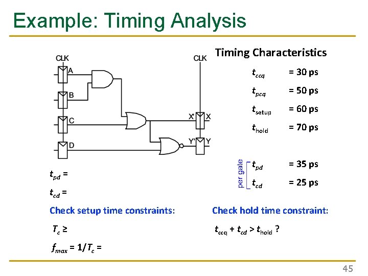
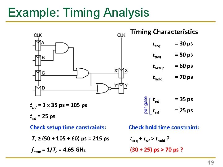
Example: Timing Analysis Timing Characteristics tpd = tccq = 30 ps tpcq = 50 ps tsetup = 60 ps thold = 70 ps tpd = 35 ps tcd = 25 ps Check setup time constraints: Check hold time constraint: Tc ≥ tccq + tcd > thold ? fmax = 1/Tc = 45

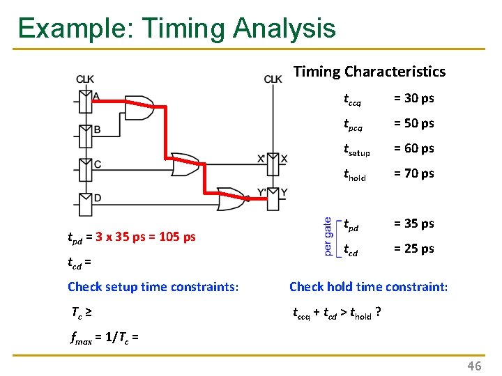
Example: Timing Analysis Timing Characteristics tpd = 3 x 35 ps = 105 ps tcd = tccq = 30 ps tpcq = 50 ps tsetup = 60 ps thold = 70 ps tpd = 35 ps tcd = 25 ps Check setup time constraints: Check hold time constraint: Tc ≥ tccq + tcd > thold ? fmax = 1/Tc = 46

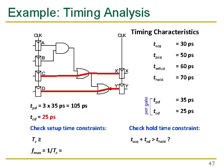
Example: Timing Analysis Timing Characteristics tpd = 3 x 35 ps = 105 ps tcd = 25 ps tccq = 30 ps tpcq = 50 ps tsetup = 60 ps thold = 70 ps tpd = 35 ps tcd = 25 ps Check setup time constraints: Check hold time constraint: Tc ≥ tccq + tcd > thold ? fmax = 1/Tc = 47

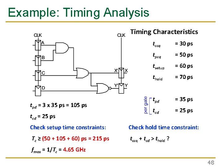
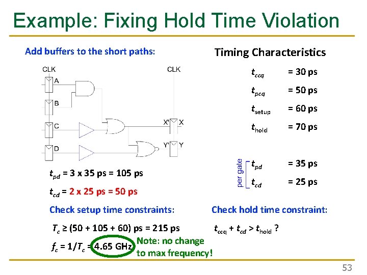
Example: Timing Analysis Timing Characteristics tpd = 3 x 35 ps = 105 ps tcd = 25 ps tccq = 30 ps tpcq = 50 ps tsetup = 60 ps thold = 70 ps tpd = 35 ps tcd = 25 ps Check setup time constraints: Check hold time constraint: Tc ≥ (50 + 105 + 60) ps = 215 ps tccq + tcd > thold ? fmax = 1/Tc = 4. 65 GHz 48

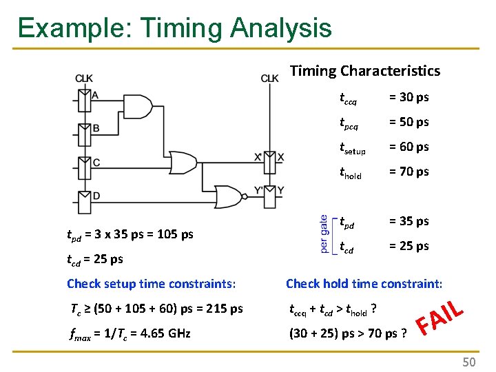
Example: Timing Analysis Timing Characteristics tpd = 3 x 35 ps = 105 ps tcd = 25 ps tccq = 30 ps tpcq = 50 ps tsetup = 60 ps thold = 70 ps tpd = 35 ps tcd = 25 ps Check setup time constraints: Check hold time constraint: Tc ≥ (50 + 105 + 60) ps = 215 ps tccq + tcd > thold ? fmax = 1/Tc = 4. 65 GHz (30 + 25) ps > 70 ps ? 49

Example: Timing Analysis Timing Characteristics tpd = 3 x 35 ps = 105 ps tcd = 25 ps tccq = 30 ps tpcq = 50 ps tsetup = 60 ps thold = 70 ps tpd = 35 ps tcd = 25 ps Check setup time constraints: Check hold time constraint: Tc ≥ (50 + 105 + 60) ps = 215 ps tccq + tcd > thold ? fmax = 1/Tc = 4. 65 GHz (30 + 25) ps > 70 ps ? L I A F 50

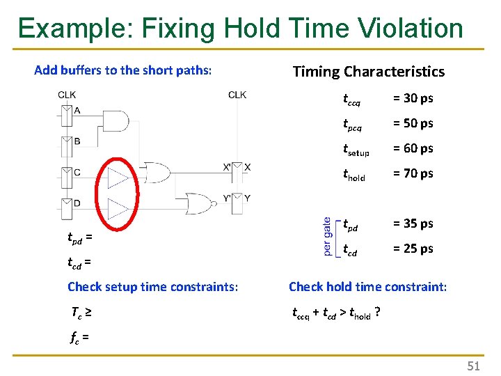
Example: Fixing Hold Time Violation Add buffers to the short paths: tpd = tcd = Timing Characteristics tccq = 30 ps tpcq = 50 ps tsetup = 60 ps thold = 70 ps tpd = 35 ps tcd = 25 ps Check setup time constraints: Check hold time constraint: Tc ≥ tccq + tcd > thold ? fc = 51

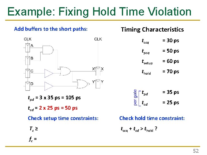
Example: Fixing Hold Time Violation Add buffers to the short paths: tpd = 3 x 35 ps = 105 ps tcd = 2 x 25 ps = 50 ps Timing Characteristics tccq = 30 ps tpcq = 50 ps tsetup = 60 ps thold = 70 ps tpd = 35 ps tcd = 25 ps Check setup time constraints: Check hold time constraint: Tc ≥ tccq + tcd > thold ? fc = 52

Example: Fixing Hold Time Violation Add buffers to the short paths: tpd = 3 x 35 ps = 105 ps tcd = 2 x 25 ps = 50 ps Check setup time constraints: Timing Characteristics tccq = 30 ps tpcq = 50 ps tsetup = 60 ps thold = 70 ps tpd = 35 ps tcd = 25 ps Check hold time constraint: tccq + tcd > thold ? Tc ≥ (50 + 105 + 60) ps = 215 ps Note: no change fc = 1/Tc = 4. 65 GHz to max frequency! 53

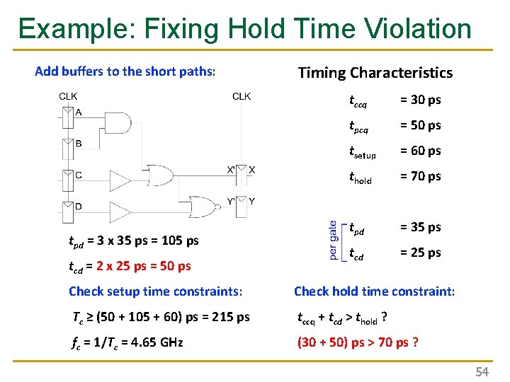
Example: Fixing Hold Time Violation Add buffers to the short paths: tpd = 3 x 35 ps = 105 ps tcd = 2 x 25 ps = 50 ps Timing Characteristics tccq = 30 ps tpcq = 50 ps tsetup = 60 ps thold = 70 ps tpd = 35 ps tcd = 25 ps Check setup time constraints: Check hold time constraint: Tc ≥ (50 + 105 + 60) ps = 215 ps tccq + tcd > thold ? fc = 1/Tc = 4. 65 GHz (30 + 50) ps > 70 ps ? 54

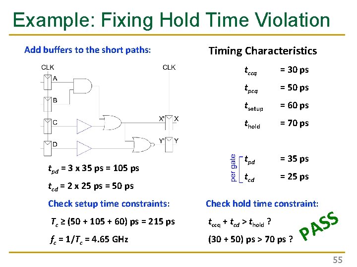
Example: Fixing Hold Time Violation Add buffers to the short paths: tpd = 3 x 35 ps = 105 ps tcd = 2 x 25 ps = 50 ps Timing Characteristics tccq = 30 ps tpcq = 50 ps tsetup = 60 ps thold = 70 ps tpd = 35 ps tcd = 25 ps Check setup time constraints: Check hold time constraint: Tc ≥ (50 + 105 + 60) ps = 215 ps tccq + tcd > thold ? fc = 1/Tc = 4. 65 GHz (30 + 50) ps > 70 ps ? S S A P 55

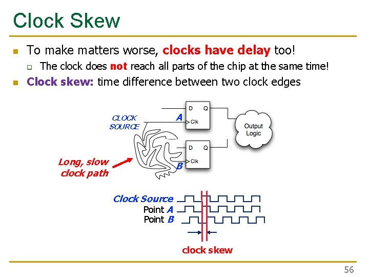
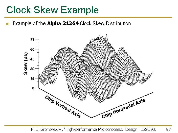
Clock Skew n To make matters worse, clocks have delay too! q n The clock does not reach all parts of the chip at the same time! Clock skew: time difference between two clock edges CLOCK SOURCE Long, slow clock path A B Clock Source Point A Point B clock skew 56

Clock Skew Example n Example of the Alpha 21264 Clock Skew Distribution P. E. Gronowski+, "High-performance Microprocessor Design, " JSSC’ 98. 57

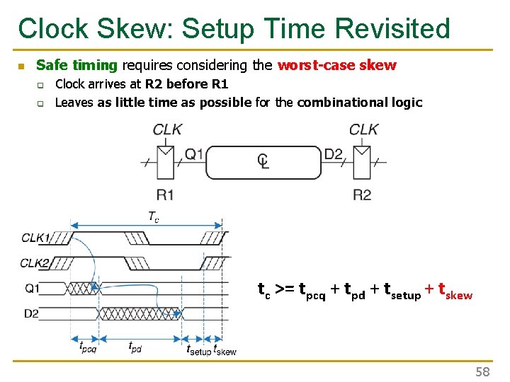
Clock Skew: Setup Time Revisited n Safe timing requires considering the worst-case skew q q Clock arrives at R 2 before R 1 Leaves as little time as possible for the combinational logic tc >= tpcq + tpd + tsetup + tskew 58

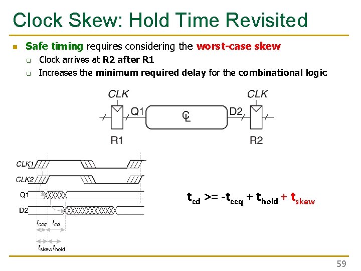
Clock Skew: Hold Time Revisited n Safe timing requires considering the worst-case skew q q Clock arrives at R 2 after R 1 Increases the minimum required delay for the combinational logic tcd >= -tccq + thold + tskew 59

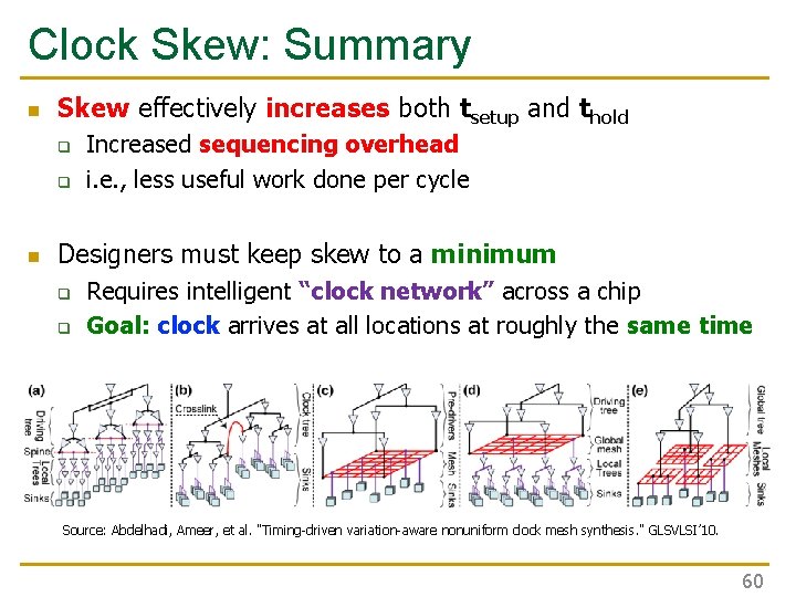
Clock Skew: Summary n Skew effectively increases both tsetup and thold q q n Increased sequencing overhead i. e. , less useful work done per cycle Designers must keep skew to a minimum q q Requires intelligent “clock network” across a chip Goal: clock arrives at all locations at roughly the same time Source: Abdelhadi, Ameer, et al. "Timing-driven variation-aware nonuniform clock mesh synthesis. " GLSVLSI’ 10. 60

Part 3: Circuit Verification 61

How Do You Know That A Circuit Works? n You have designed a circuit q q n How can you test for: q q n Is it functionally correct? Even if it is logically correct, does the hardware meet all timing constraints? Functionality? Timing? Answer: simulation tools! q q q Formal verification tools (e. g. , SAT solvers) HDL timing simulation (e. g. , Vivado) Circuit simulation (e. g. , SPICE) 62

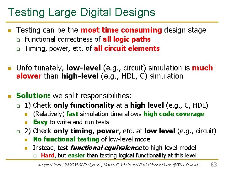
Testing Large Digital Designs n Testing can be the most time consuming design stage q q n n Functional correctness of all logic paths Timing, power, etc. of all circuit elements Unfortunately, low-level (e. g. , circuit) simulation is much slower than high-level (e. g. , HDL, C) simulation Solution: we split responsibilities: q 1) Check only functionality at a high level (e. g. , C, HDL) n n q (Relatively) fast simulation time allows high code coverage Easy to write and run tests 2) Check only timing, power, etc. at low level (e. g. , circuit) n n No functional testing of low-level model Instead, test functional equivalence to high-level model q Hard, but easier than testing logical functionality at this level Adapted from ”CMOS VLSI Design 4 e”, Neil H. E. Weste and David Money Harris © 2011 Pearson 63

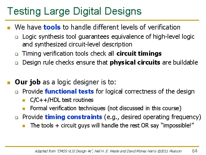
Testing Large Digital Designs n We have tools to handle different levels of verification q q q n Logic synthesis tool guarantees equivalence of high-level logic and synthesized circuit-level description Timing verification tools check all circuit timings Design rule checks ensure that physical circuits are buildable Our job as a logic designer is to: q Provide functional tests for logical correctness of the design n n q C/C++/HDL test routines Formal verification techniques (not discussed in this course) Provide timing constraints (e. g. , desired operating frequency) n The tools + circuit guys will handle the rest OR say “impossible!” Adapted from ”CMOS VLSI Design 4 e”, Neil H. E. Weste and David Money Harris © 2011 Pearson 64

Part 4: Functional Verification 65

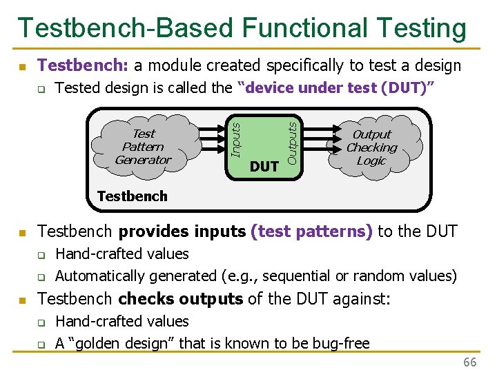
Testbench-Based Functional Testing Testbench: a module created specifically to test a design Tested design is called the “device under test (DUT)” Test Pattern Generator DUT Outputs q Inputs n Output Checking Logic Testbench n Testbench provides inputs (test patterns) to the DUT q q n Hand-crafted values Automatically generated (e. g. , sequential or random values) Testbench checks outputs of the DUT against: q q Hand-crafted values A “golden design” that is known to be bug-free 66

Testbench-Based Functional Testing n A testbench can be: q q n HDL code written to test other HDL modules Circuit schematic used to test other circuit designs The testbench is not designed for hardware synthesis! q Runs in simulation only n n q HDL simulator (e. g. , Vivado simulator) SPICE circuit simulation Testbench uses simulation-only constructs n n n E. g. , “wait 10 ns” E. g. , ideal voltage/current source Not suitable to be physically built! 67

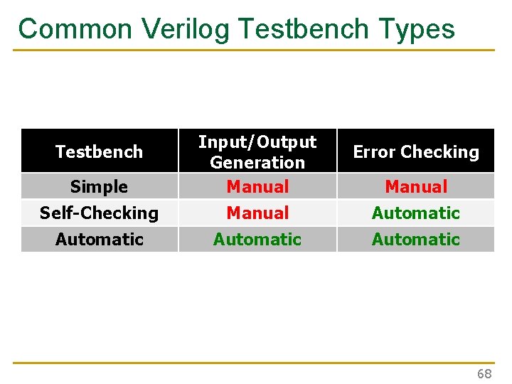
Common Verilog Testbench Types Simple Input/Output Generation Manual Self-Checking Manual Automatic Testbench Error Checking Manual 68

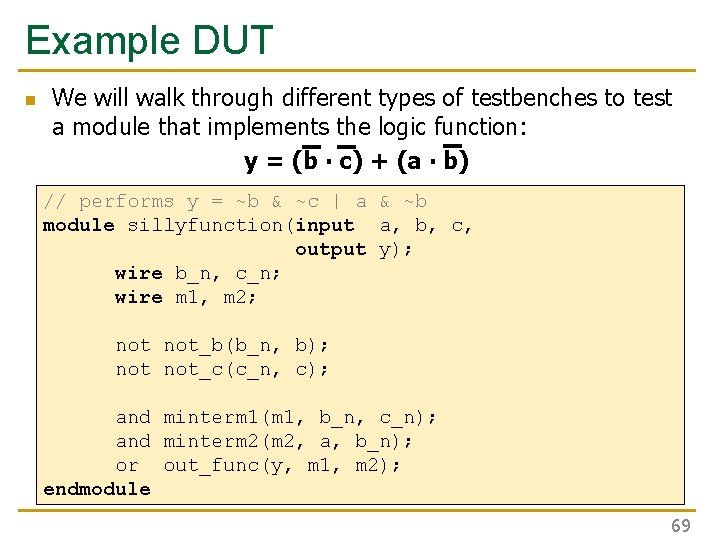
Example DUT n We will walk through different types of testbenches to test a module that implements the logic function: y = (b ∙ c) + (a ∙ b) // performs y = ~b & ~c | a & ~b module sillyfunction(input a, b, c, output y); wire b_n, c_n; wire m 1, m 2; not_b(b_n, b); not_c(c_n, c); and minterm 1(m 1, b_n, c_n); and minterm 2(m 2, a, b_n); or out_func(y, m 1, m 2); endmodule 69

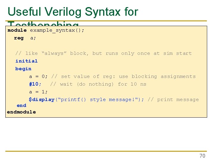
Useful Verilog Syntax for Testbenching module example_syntax(); reg a; // like “always” block, but runs only once at sim start initial begin a = 0; // set value of reg: use blocking assignments #10; // wait (do nothing) for 10 ns a = 1; $display(“printf() style message!"); // print message endmodule 70

Simple Testbench 71

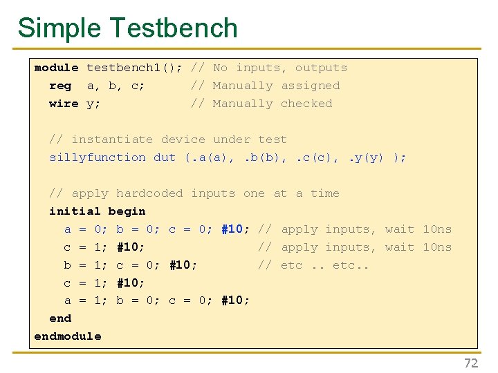
Simple Testbench module testbench 1(); // No inputs, outputs reg a, b, c; // Manually assigned wire y; // Manually checked // instantiate device under test sillyfunction dut (. a(a), . b(b), . c(c), . y(y) ); // apply hardcoded inputs one at a time initial begin a = 0; b = 0; c = 0; #10; // apply inputs, wait 10 ns c = 1; #10; // apply inputs, wait 10 ns b = 1; c = 0; #10; // etc. . c = 1; #10; a = 1; b = 0; c = 0; #10; endmodule 72

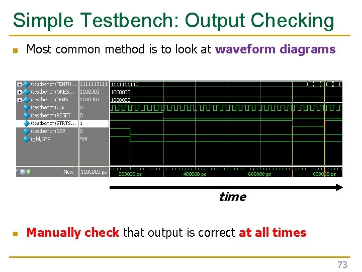
Simple Testbench: Output Checking n Most common method is to look at waveform diagrams time n Manually check that output is correct at all times 73

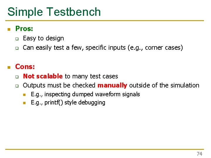
Simple Testbench n Pros: q q n Easy to design Can easily test a few, specific inputs (e. g. , corner cases) Cons: q q Not scalable to many test cases Outputs must be checked manually outside of the simulation n n E. g. , inspecting dumped waveform signals E. g. , printf() style debugging 74

Self-Checking Testbench 75

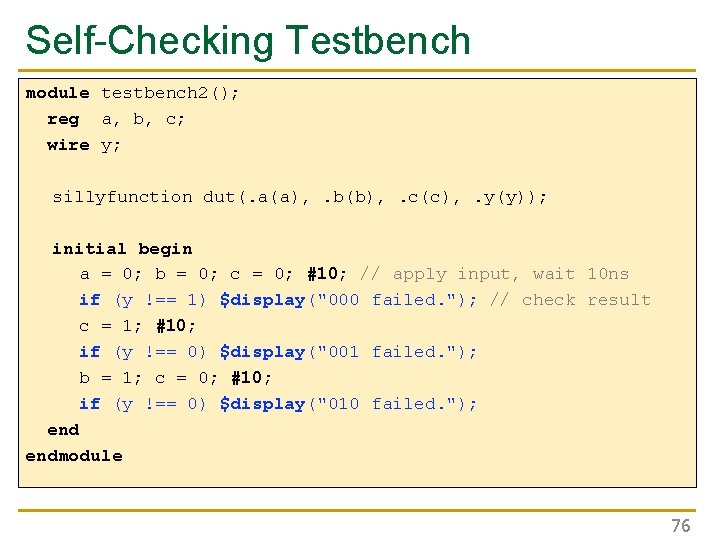
Self-Checking Testbench module testbench 2(); reg a, b, c; wire y; sillyfunction dut(. a(a), . b(b), . c(c), . y(y)); initial begin a = 0; b = 0; c = 0; #10; // apply input, wait 10 ns if (y !== 1) $display("000 failed. "); // check result c = 1; #10; if (y !== 0) $display("001 failed. "); b = 1; c = 0; #10; if (y !== 0) $display("010 failed. "); endmodule 76

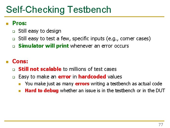
Self-Checking Testbench n Pros: q q q n Still easy to design Still easy to test a few, specific inputs (e. g. , corner cases) Simulator will print whenever an error occurs Cons: q q Still not scalable to millions of test cases Easy to make an error in hardcoded values n n You make just as many errors writing a testbench as actual code Hard to debug whether an issue is in the testbench or in the DUT 77

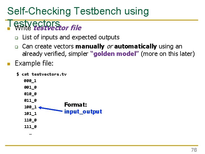
Self-Checking Testbench using Testvectors n Write testvector file q q n List of inputs and expected outputs Can create vectors manually or automatically using an already verified, simpler “golden model” (more on this later) Example file: $ cat testvectors. tv 000_1 001_0 010_0 011_0 Format: 100_1 input_output 101_1 110_0 111_0 … 78

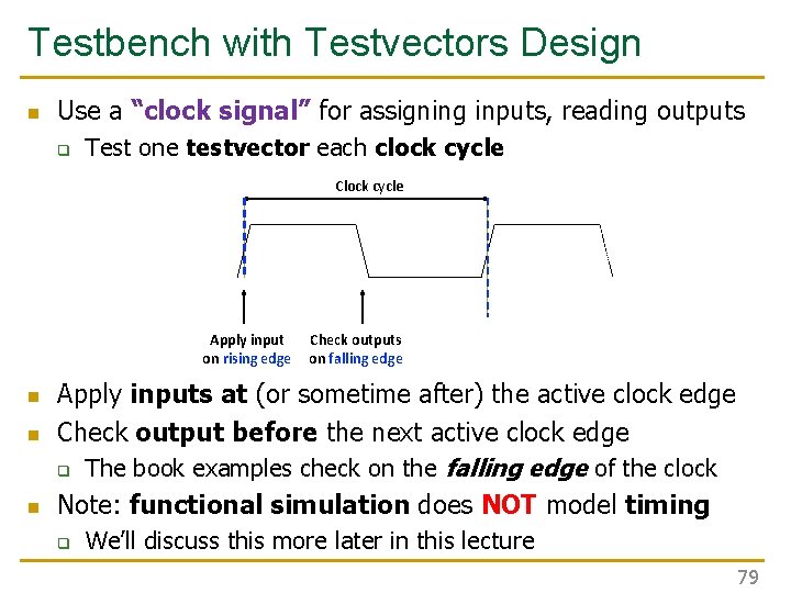
Testbench with Testvectors Design n Use a “clock signal” for assigning inputs, reading outputs q Test one testvector each clock cycle Clock cycle Apply input on rising edge n n n Check outputs on falling edge Apply inputs at (or sometime after) the active clock edge Check output before the next active clock edge q The book examples check on the falling edge of the clock Note: functional simulation does NOT model timing q We’ll discuss this more later in this lecture 79

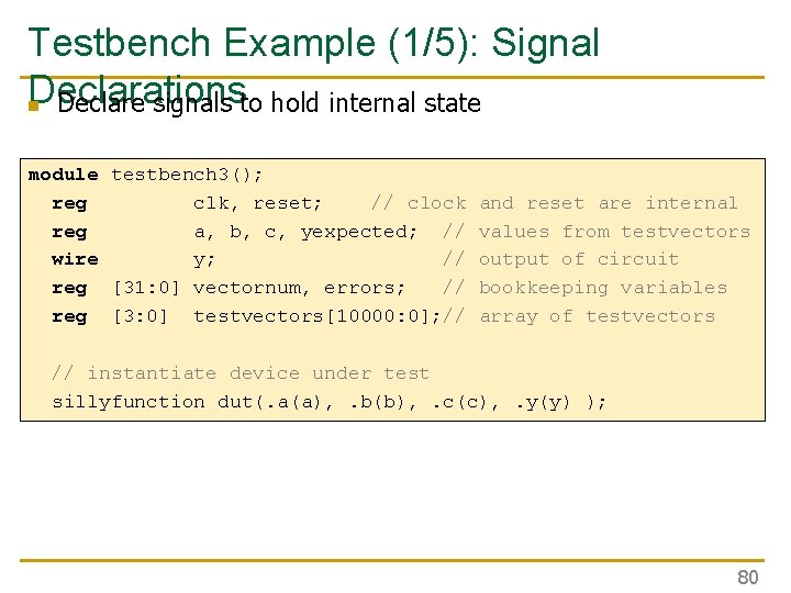
Testbench Example (1/5): Signal Declarations n Declare signals to hold internal state module testbench 3(); reg clk, reset; // clock reg a, b, c, yexpected; // wire y; // reg [31: 0] vectornum, errors; // reg [3: 0] testvectors[10000: 0]; // and reset are internal values from testvectors output of circuit bookkeeping variables array of testvectors // instantiate device under test sillyfunction dut(. a(a), . b(b), . c(c), . y(y) ); 80

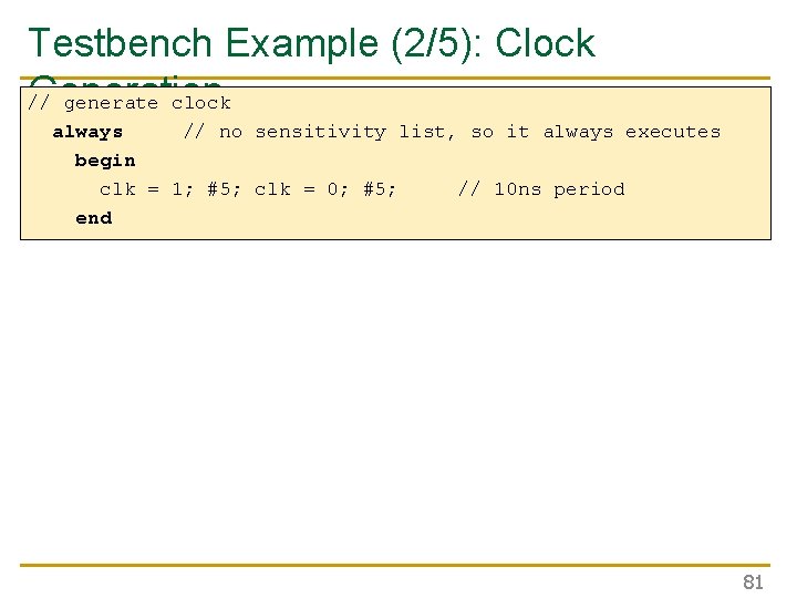
Testbench Example (2/5): Clock Generation // generate clock always // no sensitivity list, so it always executes begin clk = 1; #5; clk = 0; #5; // 10 ns period end 81

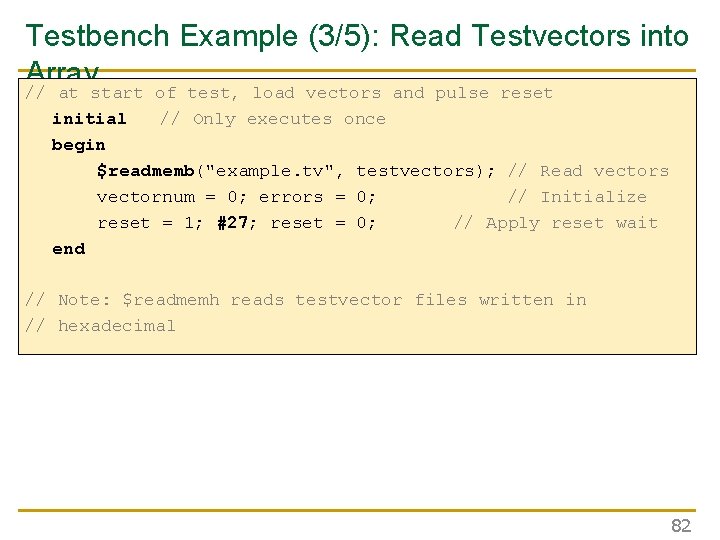
Testbench Example (3/5): Read Testvectors into Array // at start of test, load vectors and pulse reset initial // Only executes once begin $readmemb("example. tv", testvectors); // Read vectors vectornum = 0; errors = 0; // Initialize reset = 1; #27; reset = 0; // Apply reset wait end // Note: $readmemh reads testvector files written in // hexadecimal 82

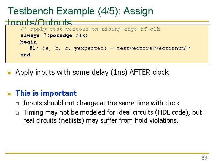
Testbench Example (4/5): Assign Inputs/Outputs // apply test vectors on rising edge of clk always @(posedge clk) begin #1; {a, b, c, yexpected} = testvectors[vectornum]; end n Apply inputs with some delay (1 ns) AFTER clock n This is important q q Inputs should not change at the same time with clock Timing may not be modeled for ideal circuits (HDL code), but real circuits (netlists) may suffer from hold violations. 83

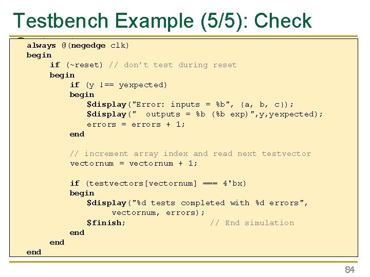
Testbench Example (5/5): Check Outputs always @(negedge clk) begin if (~reset) // don’t test during reset begin if (y !== yexpected) begin $display("Error: inputs = %b", {a, b, c}); $display(" outputs = %b (%b exp)", y, yexpected); errors = errors + 1; end // increment array index and read next testvectornum = vectornum + 1; if (testvectors[vectornum] === 4'bx) begin $display("%d tests completed with %d errors", vectornum, errors); $finish; // End simulation end end 84

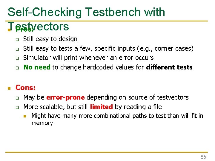
Self-Checking Testbench with Testvectors n Pros: q q n Still easy to design Still easy to tests a few, specific inputs (e. g. , corner cases) Simulator will print whenever an error occurs No need to change hardcoded values for different tests Cons: q q May be error-prone depending on source of testvectors More scalable, but still limited by reading a file n Might have many more combinational paths to test than will fit in memory 85

Automatic Testbench 86

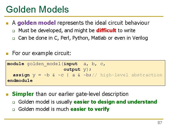
Golden Models n A golden model represents the ideal circuit behaviour q q n Must be developed, and might be difficult to write Can be done in C, Perl, Python, Matlab or even in Verilog For our example circuit: module golden_model(input a, b, c, output y); assign y = ~b & ~c | a & ~b; // high-level abstraction endmodule n Simpler than our earlier gate-level description q q Golden model is usually easier to design and understand Golden model is much easier to verify 87

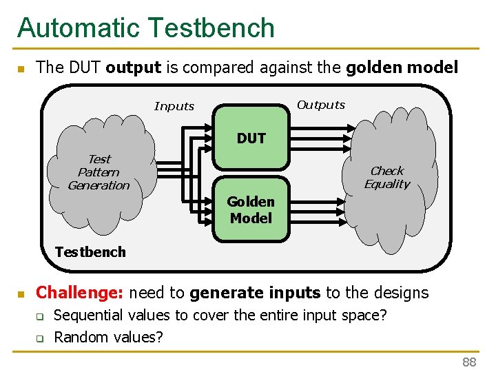
Automatic Testbench n The DUT output is compared against the golden model Outputs Inputs DUT Test Pattern Generation Check Equality Golden Model Testbench n Challenge: need to generate inputs to the designs q q Sequential values to cover the entire input space? Random values? 88

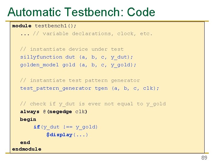
Automatic Testbench: Code module testbench 1(); . . . // variable declarations, clock, etc. // instantiate device under test sillyfunction dut (a, b, c, y_dut); golden_model gold (a, b, c, y_gold); // instantiate test pattern generator test_pattern_generator tgen (a, b, c, clk); // check if y_dut is ever not equal to y_gold always @(negedge clk) begin if(y_dut !== y_gold) $display(. . . ) endmodule 89

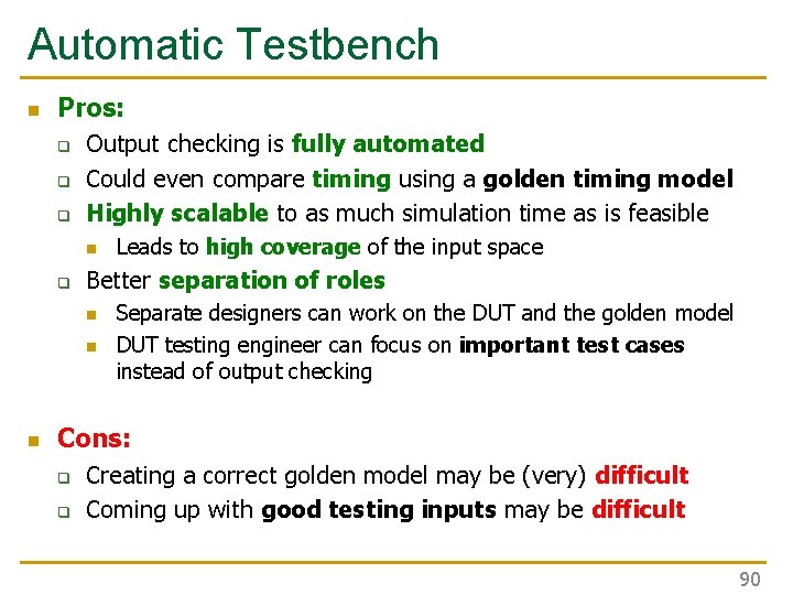
Automatic Testbench n Pros: q q q Output checking is fully automated Could even compare timing using a golden timing model Highly scalable to as much simulation time as is feasible n q Better separation of roles n n n Leads to high coverage of the input space Separate designers can work on the DUT and the golden model DUT testing engineer can focus on important test cases instead of output checking Cons: q q Creating a correct golden model may be (very) difficult Coming up with good testing inputs may be difficult 90

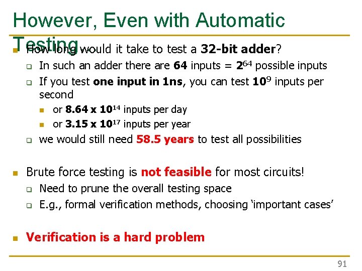
However, Even with Automatic Testing… n How long would it take to test a 32 -bit adder? q q In such an adder there are 64 inputs = 264 possible inputs If you test one input in 1 ns, you can test 109 inputs per second n n q n we would still need 58. 5 years to test all possibilities Brute force testing is not feasible for most circuits! q q n or 8. 64 x 1014 inputs per day or 3. 15 x 1017 inputs per year Need to prune the overall testing space E. g. , formal verification methods, choosing ‘important cases’ Verification is a hard problem 91

Part 5: Timing Verification 92

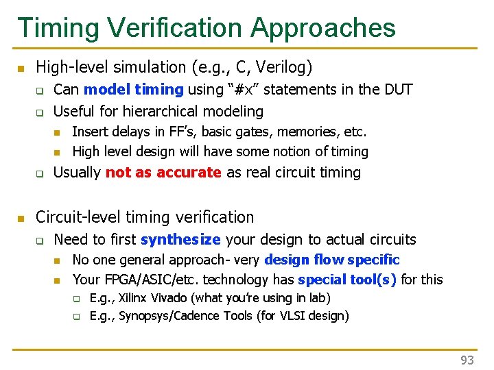
Timing Verification Approaches n High-level simulation (e. g. , C, Verilog) q q Can model timing using “#x” statements in the DUT Useful for hierarchical modeling n n q n Insert delays in FF’s, basic gates, memories, etc. High level design will have some notion of timing Usually not as accurate as real circuit timing Circuit-level timing verification q Need to first synthesize your design to actual circuits n n No one general approach- very design flow specific Your FPGA/ASIC/etc. technology has special tool(s) for this q q E. g. , Xilinx Vivado (what you’re using in lab) E. g. , Synopsys/Cadence Tools (for VLSI design) 93

The Good News n Tools will try to meet timing for you! q q q n Setup times, hold times Clock skews … Usually it generates a ‘timing report’ or ‘timing summary’ q q q Provides worst-case delay paths Maximum operation frequency Any timing errors that were found 94

The Bad News n The tool can fail to find a solution q Desired clock frequency is too aggressive n q Too much logic on clock paths n q n Introduces excessive clock skew Timing issues with asynchronous logic The tool will provide (hopefully) helpful errors q q n Can result in setup time violation on a particularly long path Reports will contain paths that failed to meet timing Gives a place from where to start debugging Q: How can we fix timing errors? 95

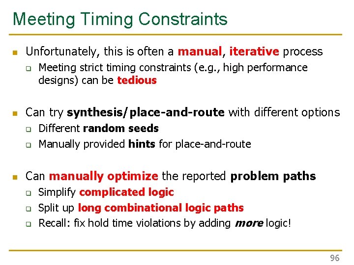
Meeting Timing Constraints n Unfortunately, this is often a manual, iterative process q n Can try synthesis/place-and-route with different options q q n Meeting strict timing constraints (e. g. , high performance designs) can be tedious Different random seeds Manually provided hints for place-and-route Can manually optimize the reported problem paths q q q Simplify complicated logic Split up long combinational logic paths Recall: fix hold time violations by adding more logic! 96

Lecture Summary n Timing in combinational circuits q q n Timing in sequential circuits q q n Propagation delay and contamination delay Glitches Setup time and hold time Determining how fast a circuit can operate Circuit Verification q q q How to make sure a circuit works correctly Functional verification Timing verification 97

Design of Digital Circuits Lecture 8: Timing and Verification Prof. Onur Mutlu ETH Zurich Spring 2018 16 March 2018