Cpr E 281 Digital Logic Instructor Alexander Stoytchev


![Building an AND gate with NAND gates [http: //en. wikipedia. org/wiki/NAND_logic] Building an AND gate with NAND gates [http: //en. wikipedia. org/wiki/NAND_logic]](https://slidetodoc.com/presentation_image/2d8fdc5d1f7a40ae5eb867ae3999d0b9/image-26.jpg)
![Building an OR gate with NAND gates [http: //en. wikipedia. org/wiki/NAND_logic] Building an OR gate with NAND gates [http: //en. wikipedia. org/wiki/NAND_logic]](https://slidetodoc.com/presentation_image/2d8fdc5d1f7a40ae5eb867ae3999d0b9/image-27.jpg)
![NOR gate with NAND gates [http: //en. wikipedia. org/wiki/NAND_logic] NOR gate with NAND gates [http: //en. wikipedia. org/wiki/NAND_logic]](https://slidetodoc.com/presentation_image/2d8fdc5d1f7a40ae5eb867ae3999d0b9/image-29.jpg)
![XOR gate with NAND gates [http: //en. wikipedia. org/wiki/NAND_logic] XOR gate with NAND gates [http: //en. wikipedia. org/wiki/NAND_logic]](https://slidetodoc.com/presentation_image/2d8fdc5d1f7a40ae5eb867ae3999d0b9/image-30.jpg)
![XNOR gate with NAND gates [http: //en. wikipedia. org/wiki/NAND_logic] XNOR gate with NAND gates [http: //en. wikipedia. org/wiki/NAND_logic]](https://slidetodoc.com/presentation_image/2d8fdc5d1f7a40ae5eb867ae3999d0b9/image-31.jpg)


![Building an OR gate with NOR gates [http: //en. wikipedia. org/wiki/NOR_logic] Building an OR gate with NOR gates [http: //en. wikipedia. org/wiki/NOR_logic]](https://slidetodoc.com/presentation_image/2d8fdc5d1f7a40ae5eb867ae3999d0b9/image-36.jpg)
![NAND gate with NOR gates [http: //en. wikipedia. org/wiki/NOR_logic] NAND gate with NOR gates [http: //en. wikipedia. org/wiki/NOR_logic]](https://slidetodoc.com/presentation_image/2d8fdc5d1f7a40ae5eb867ae3999d0b9/image-39.jpg)
![XOR gate with NOR gates [http: //en. wikipedia. org/wiki/NOR_logic] XOR gate with NOR gates [http: //en. wikipedia. org/wiki/NOR_logic]](https://slidetodoc.com/presentation_image/2d8fdc5d1f7a40ae5eb867ae3999d0b9/image-40.jpg)
![XNOR gate with NOR gates [http: //en. wikipedia. org/wiki/NOR_logic] XNOR gate with NOR gates [http: //en. wikipedia. org/wiki/NOR_logic]](https://slidetodoc.com/presentation_image/2d8fdc5d1f7a40ae5eb867ae3999d0b9/image-41.jpg)
![[ Platt 2009 ] [ Platt 2009 ]](https://slidetodoc.com/presentation_image/2d8fdc5d1f7a40ae5eb867ae3999d0b9/image-43.jpg)
![[ Platt 2009 ] [ Platt 2009 ]](https://slidetodoc.com/presentation_image/2d8fdc5d1f7a40ae5eb867ae3999d0b9/image-44.jpg)
![[ Platt 2009 ] [ Platt 2009 ]](https://slidetodoc.com/presentation_image/2d8fdc5d1f7a40ae5eb867ae3999d0b9/image-45.jpg)







- Slides: 77

Cpr. E 281: Digital Logic Instructor: Alexander Stoytchev http: //www. ece. iastate. edu/~alexs/classes/

NAND and NOR Logic Networks Cpr. E 281: Digital Logic Iowa State University, Ames, IA Copyright © Alexander Stoytchev

Administrative Stuff • HW 2 is due today

Administrative Stuff • HW 3 is out • It is due on Monday Feb 3 @ 4 pm. • Please write clearly on the first page (in BLOCK CAPITAL letters) the following three things: § Your First and Last Name § Your Student ID Number § Your Lab Section Letter • Also, please § Staple your pages § Use Letter-sized sheets

Quick Review

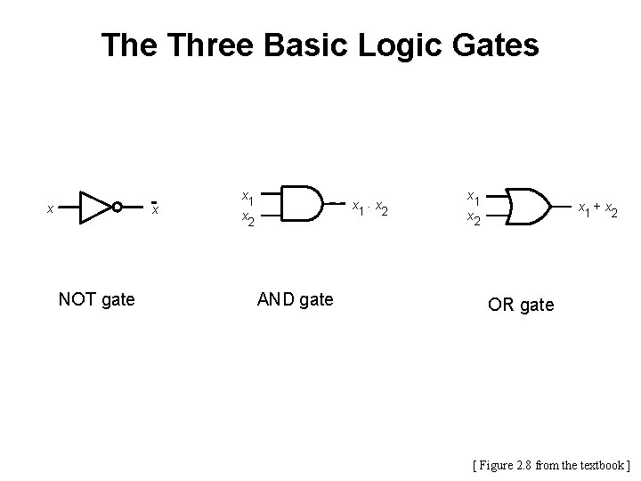
The Three Basic Logic Gates x x NOT gate x 1 x 2 x 1 × x 2 AND gate x 1 x 2 x 1 + x 2 OR gate [ Figure 2. 8 from the textbook ]

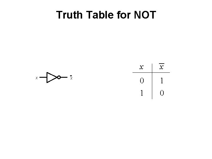
Truth Table for NOT x x 0 1 1 0

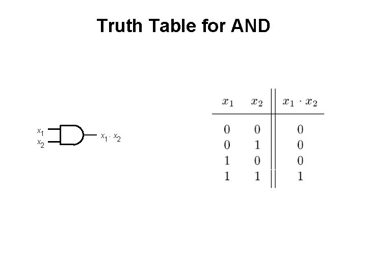
Truth Table for AND x 1 x 2 x 1 × x 2

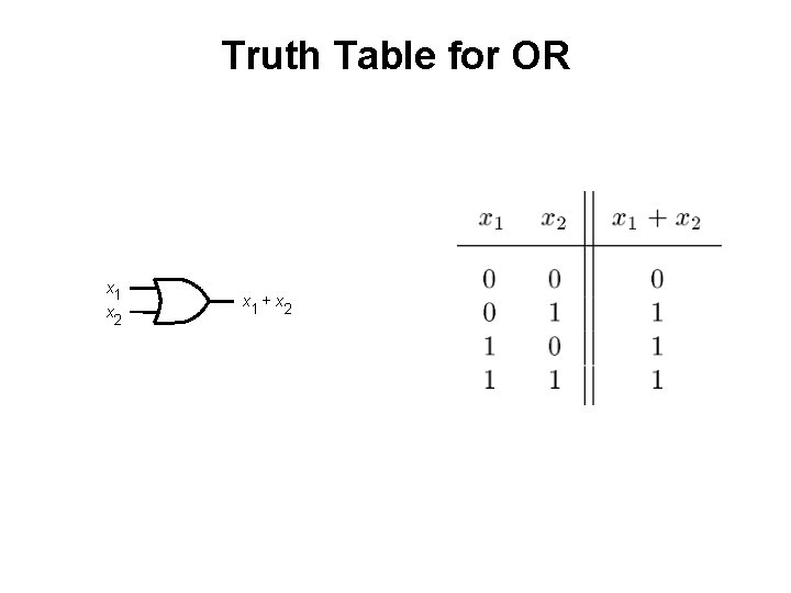
Truth Table for OR x 1 x 2 x 1 + x 2

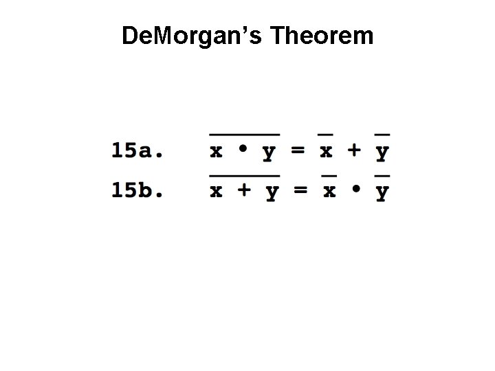
De. Morgan’s Theorem

Two New Logic Gates

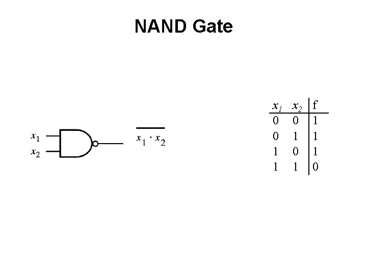
NAND Gate x 1 0 0 1 1 x 2 0 1 f 1 1 1 0

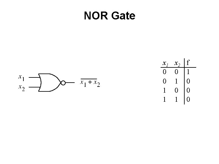
NOR Gate x 1 0 0 1 1 x 2 0 1 f 1 0 0 0

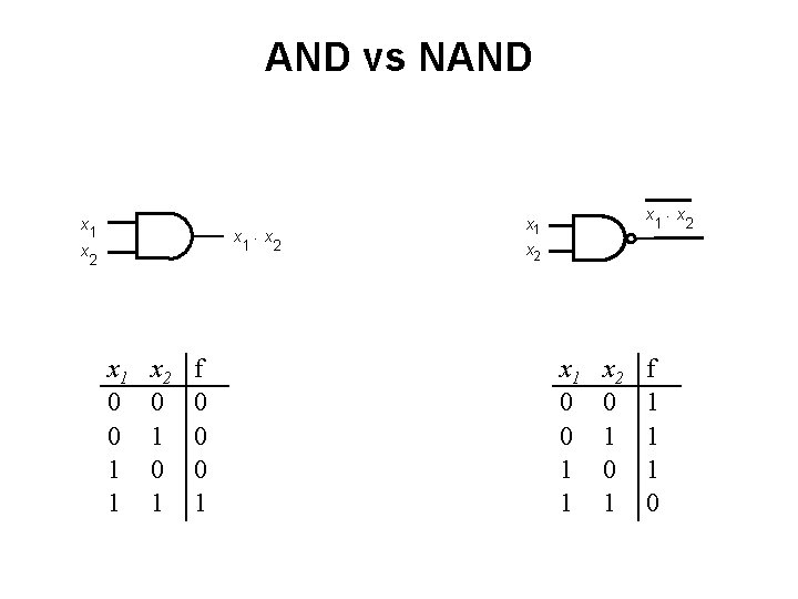
AND vs NAND x x 1 x ×x 1 2 2 x 1 0 0 1 1 x 2 0 1 f 0 0 0 1 x ×x 1 2 x 1 x 2 x 1 0 0 1 1 x 2 0 1 f 1 1 1 0

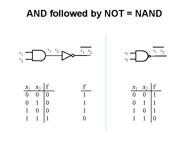
AND followed by NOT = NAND x x x ×x 1 2 1 x ×x 1 2 x 1 x 2 2 x 1 0 0 1 1 x 2 0 1 f 0 0 0 1 f 1 1 1 0 x 1 0 0 1 1 x 2 0 1 f 1 1 1 0

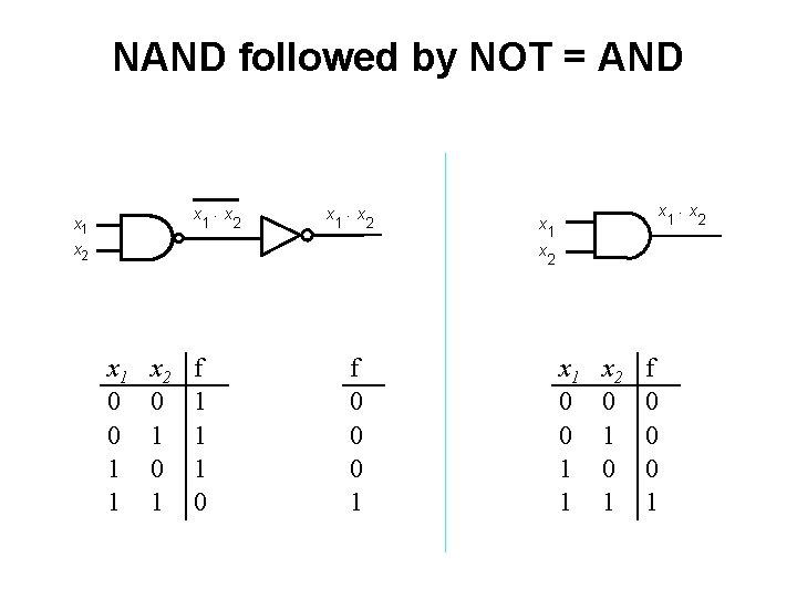
NAND followed by NOT = AND x ×x 1 2 x 1 x ×x 1 2 x x x 1 0 0 1 1 x 2 0 1 f 1 1 1 0 f 0 0 0 1 x ×x 1 2 x 1 0 0 1 1 x 2 0 1 f 0 0 0 1

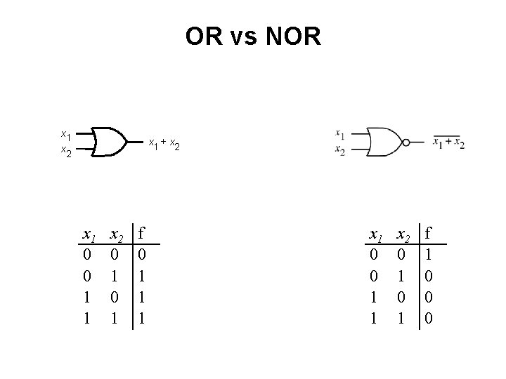
OR vs NOR x 1 x 2 x 1 + x 2 x 1 0 0 1 1 x 2 0 1 f 0 1 1 1 x 1 0 0 1 1 x 2 0 1 f 1 0 0 0

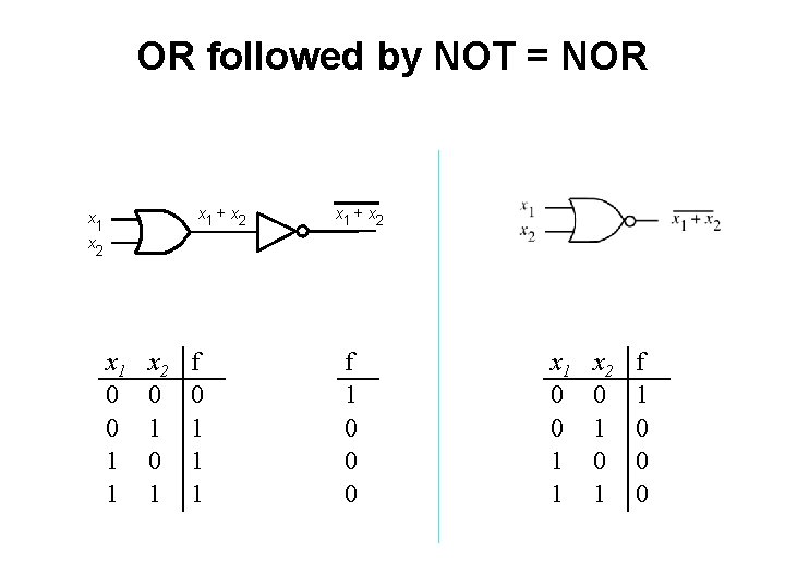
OR followed by NOT = NOR x 1 + x 2 x 1 0 0 1 1 x 2 0 1 f 0 1 1 1 x 1 + x 2 f 1 0 0 0 x 1 0 0 1 1 x 2 0 1 f 1 0 0 0

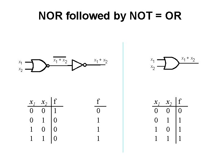
NOR followed by NOT = OR x 1 + x 2 x 1 0 0 1 1 x 2 0 1 f 1 0 0 0 f 0 1 1 1 x 1 + x 2 x 1 0 0 1 1 x 2 0 1 f 0 1 1 1

Why do we need two more gates?

Why do we need two more gates? They can be implemented with fewer transistors. (more about this later)

They are simpler to implement, but are they also useful?

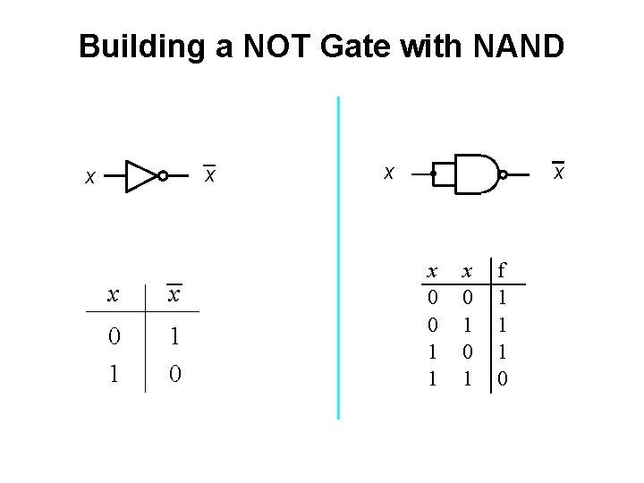
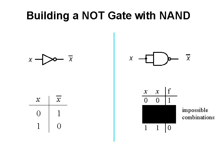
Building a NOT Gate with NAND x x 0 1 1 0 x x x 0 0 1 1 x 0 1 f 1 1 1 0

Building a NOT Gate with NAND x x x 0 1 x 1 0 x x x 0 0 1 1 x 0 1 f 1 1 1 0 impossible combinations

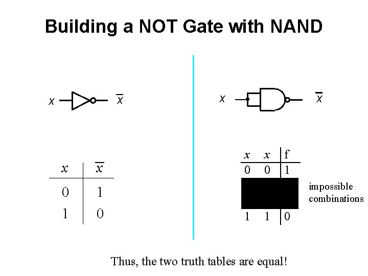
Building a NOT Gate with NAND x x x 0 1 x 1 0 x x x 0 0 1 1 x 0 1 f 1 1 1 0 Thus, the two truth tables are equal! impossible combinations
![Building an AND gate with NAND gates http en wikipedia orgwikiNANDlogic Building an AND gate with NAND gates [http: //en. wikipedia. org/wiki/NAND_logic]](https://slidetodoc.com/presentation_image/2d8fdc5d1f7a40ae5eb867ae3999d0b9/image-26.jpg)
Building an AND gate with NAND gates [http: //en. wikipedia. org/wiki/NAND_logic]
![Building an OR gate with NAND gates http en wikipedia orgwikiNANDlogic Building an OR gate with NAND gates [http: //en. wikipedia. org/wiki/NAND_logic]](https://slidetodoc.com/presentation_image/2d8fdc5d1f7a40ae5eb867ae3999d0b9/image-27.jpg)
Building an OR gate with NAND gates [http: //en. wikipedia. org/wiki/NAND_logic]

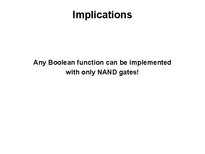
Implications Any Boolean function can be implemented with only NAND gates!
![NOR gate with NAND gates http en wikipedia orgwikiNANDlogic NOR gate with NAND gates [http: //en. wikipedia. org/wiki/NAND_logic]](https://slidetodoc.com/presentation_image/2d8fdc5d1f7a40ae5eb867ae3999d0b9/image-29.jpg)
NOR gate with NAND gates [http: //en. wikipedia. org/wiki/NAND_logic]
![XOR gate with NAND gates http en wikipedia orgwikiNANDlogic XOR gate with NAND gates [http: //en. wikipedia. org/wiki/NAND_logic]](https://slidetodoc.com/presentation_image/2d8fdc5d1f7a40ae5eb867ae3999d0b9/image-30.jpg)
XOR gate with NAND gates [http: //en. wikipedia. org/wiki/NAND_logic]
![XNOR gate with NAND gates http en wikipedia orgwikiNANDlogic XNOR gate with NAND gates [http: //en. wikipedia. org/wiki/NAND_logic]](https://slidetodoc.com/presentation_image/2d8fdc5d1f7a40ae5eb867ae3999d0b9/image-31.jpg)
XNOR gate with NAND gates [http: //en. wikipedia. org/wiki/NAND_logic]


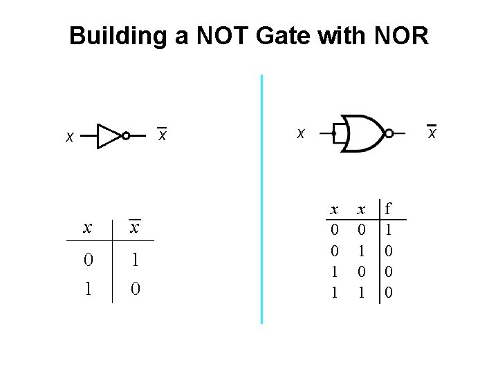
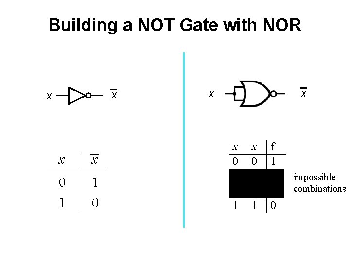
Building a NOT Gate with NOR x x 0 1 1 0 x x x 0 0 1 1 x 0 1 f 1 0 0 0

Building a NOT Gate with NOR x x x 0 1 x 1 0 x x x 0 0 1 1 x 0 1 f 1 0 0 0 impossible combinations

Building a NOT Gate with NOR x x x 0 1 x 1 0 x x x 0 0 1 1 x 0 1 f 1 0 0 0 Thus, the two truth tables are equal! impossible combinations
![Building an OR gate with NOR gates http en wikipedia orgwikiNORlogic Building an OR gate with NOR gates [http: //en. wikipedia. org/wiki/NOR_logic]](https://slidetodoc.com/presentation_image/2d8fdc5d1f7a40ae5eb867ae3999d0b9/image-36.jpg)
Building an OR gate with NOR gates [http: //en. wikipedia. org/wiki/NOR_logic]

Let’s build an AND gate with NOR gates

Implications Any Boolean function can be implemented with only NOR gates!
![NAND gate with NOR gates http en wikipedia orgwikiNORlogic NAND gate with NOR gates [http: //en. wikipedia. org/wiki/NOR_logic]](https://slidetodoc.com/presentation_image/2d8fdc5d1f7a40ae5eb867ae3999d0b9/image-39.jpg)
NAND gate with NOR gates [http: //en. wikipedia. org/wiki/NOR_logic]
![XOR gate with NOR gates http en wikipedia orgwikiNORlogic XOR gate with NOR gates [http: //en. wikipedia. org/wiki/NOR_logic]](https://slidetodoc.com/presentation_image/2d8fdc5d1f7a40ae5eb867ae3999d0b9/image-40.jpg)
XOR gate with NOR gates [http: //en. wikipedia. org/wiki/NOR_logic]
![XNOR gate with NOR gates http en wikipedia orgwikiNORlogic XNOR gate with NOR gates [http: //en. wikipedia. org/wiki/NOR_logic]](https://slidetodoc.com/presentation_image/2d8fdc5d1f7a40ae5eb867ae3999d0b9/image-41.jpg)
XNOR gate with NOR gates [http: //en. wikipedia. org/wiki/NOR_logic]

The following examples came from this book
![Platt 2009 [ Platt 2009 ]](https://slidetodoc.com/presentation_image/2d8fdc5d1f7a40ae5eb867ae3999d0b9/image-43.jpg)
[ Platt 2009 ]
![Platt 2009 [ Platt 2009 ]](https://slidetodoc.com/presentation_image/2d8fdc5d1f7a40ae5eb867ae3999d0b9/image-44.jpg)
[ Platt 2009 ]
![Platt 2009 [ Platt 2009 ]](https://slidetodoc.com/presentation_image/2d8fdc5d1f7a40ae5eb867ae3999d0b9/image-45.jpg)
[ Platt 2009 ]

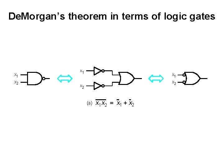
De. Morgan’s theorem in terms of logic gates x 1 x 2 (a) x 1 x 2 = x 1 + x 2

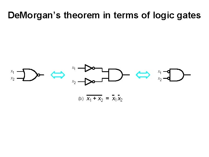
De. Morgan’s theorem in terms of logic gates x 1 x 2 (b) x 1 + x 2 = x 1 x 2

Function Synthesis

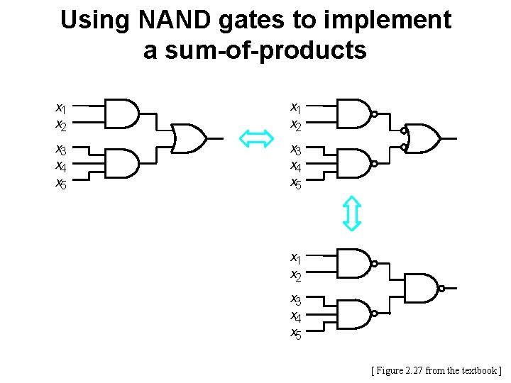
Using NAND gates to implement a sum-of-products x 1 x 2 x 3 x 4 x 5 [ Figure 2. 27 from the textbook ]

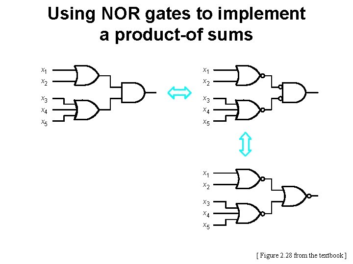
Using NOR gates to implement a product-of sums x 1 x 2 x 3 x 4 x 5 [ Figure 2. 28 from the textbook ]

Example 2. 13

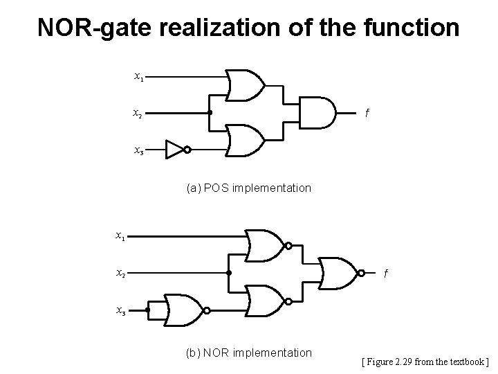
NOR-gate realization of the function x 1 x 2 f x 3 (a) POS implementation x 1 x 2 f x 3 (b) NOR implementation [ Figure 2. 29 from the textbook ]

Example 2. 10

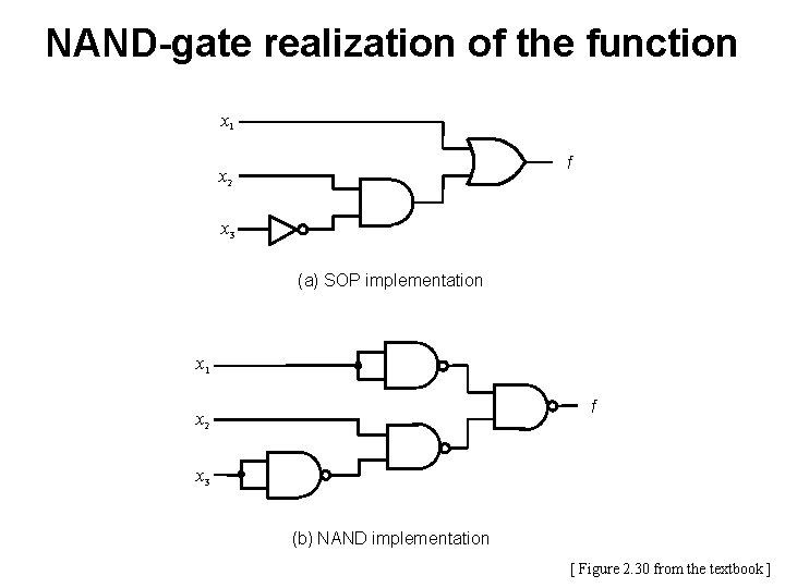
NAND-gate realization of the function x 1 f x 2 x 3 (a) SOP implementation x 1 f x 2 x 3 (b) NAND implementation [ Figure 2. 30 from the textbook ]


Appendix B Implementation Technology

Figure B. 1. Logic values as voltage levels.

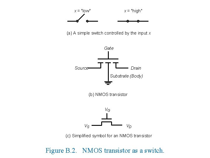
x = "low" x = "high" (a) A simple switch controlled by the input x Gate Source Drain Substrate (Body) (b) NMOS transistor VG VS VD (c) Simplified symbol for an NMOS transistor Figure B. 2. NMOS transistor as a switch.

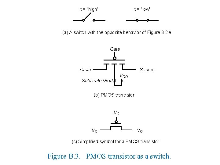
x = "high" x = "low" (a) A switch with the opposite behavior of Figure 3. 2 a Gate Drain Source Substrate (Body) VDD (b) PMOS transistor VG VS VD (c) Simplified symbol for a PMOS transistor Figure B. 3. PMOS transistor as a switch.

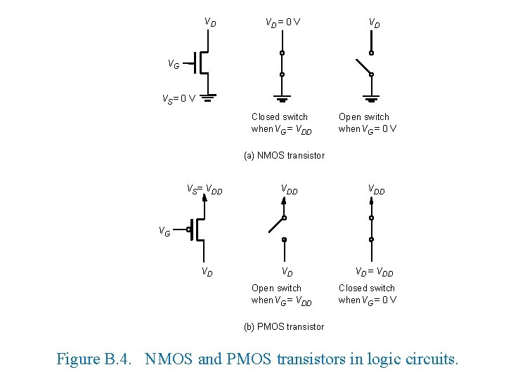
VD VD = 0 V VD VG VS = 0 V Closed switch when. VG = VDD Open switch when. VG = 0 V (a) NMOS transistor VS = VDD VDD VD VD VD = VDD VG Open switch when. VG = VDD Closed switch when. VG = 0 V (b) PMOS transistor Figure B. 4. NMOS and PMOS transistors in logic circuits.

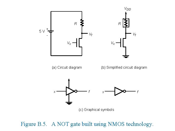
VDD R 5 V R + Vf - Vf Vx Vx (a) Circuit diagram x (b) Simplified circuit diagram f x f (c) Graphical symbols Figure B. 5. A NOT gate built using NMOS technology.

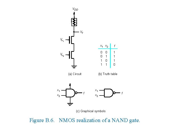
VDD Vf Vx 1 Vx 2 (a) Circuit x 1 x 2 f 0 0 1 1 1 0 0 1 (b) Truth table f x 1 x 2 f (c) Graphical symbols Figure B. 6. NMOS realization of a NAND gate.

Figure B. 7. NMOS realization of a NOR gate.

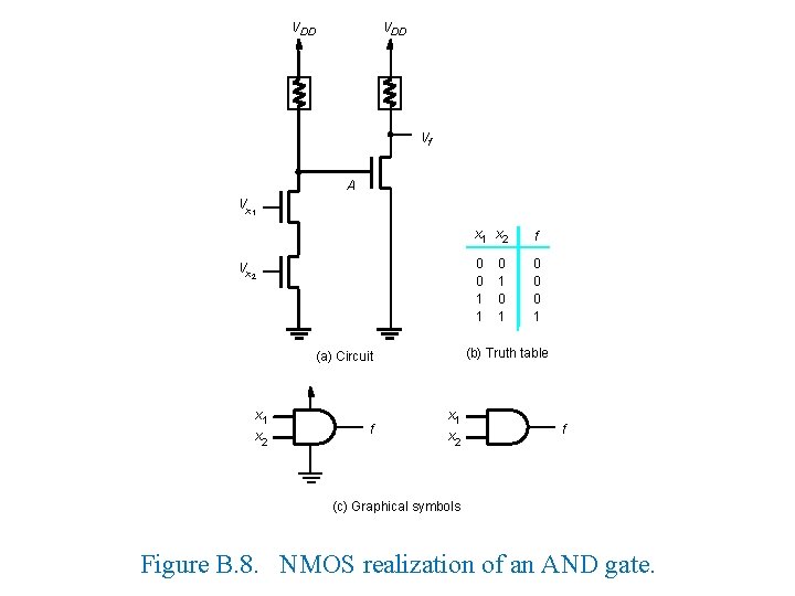
VDD Vf A Vx 1 Vx 2 f f 0 0 1 1 0 0 0 1 0 1 (b) Truth table (a) Circuit x 1 x 2 f (c) Graphical symbols Figure B. 8. NMOS realization of an AND gate.

Figure B. 9. NMOS realization of an OR gate.

Figure B. 10. Structure of an NMOS circuit.

Figure B. 11. Structure of a CMOS circuit.

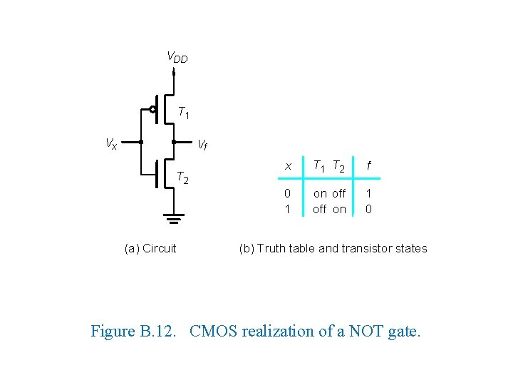
VDD T 1 Vx Vf T 2 (a) Circuit x T 1 T 2 f 0 1 on off on 1 0 (b) Truth table and transistor states Figure B. 12. CMOS realization of a NOT gate.

Figure B. 13. CMOS realization of a NAND gate.

Figure B. 14. CMOS realization of a NOR gate.

Figure B. 15. CMOS realization of an AND gate.


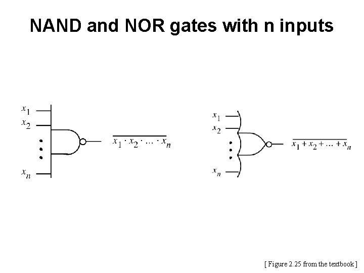
NAND and NOR gates with n inputs [ Figure 2. 25 from the textbook ]

Figure B. 57. High fan-in NMOS NAND gate.

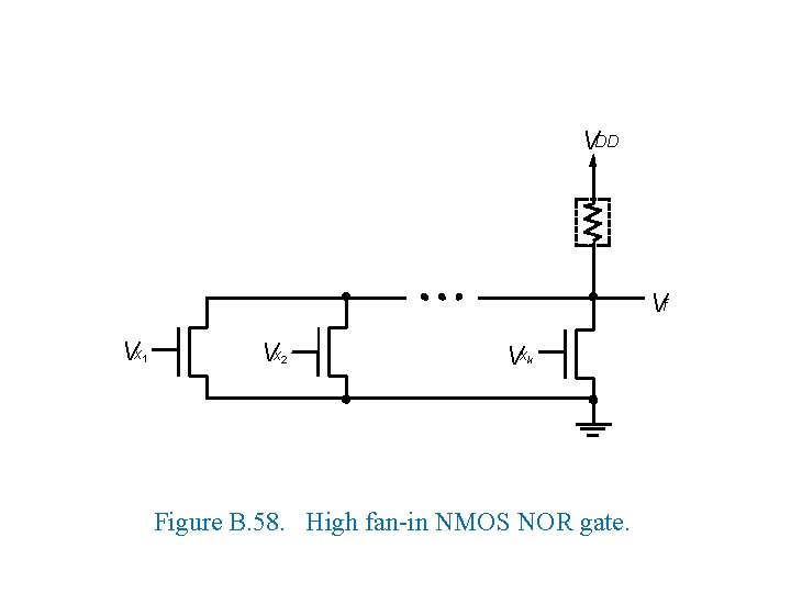
VDD Vf Vx 1 Vx 2 Vxk Figure B. 58. High fan-in NMOS NOR gate.

Questions?

THE END