Cpr E 281 Digital Logic Instructor Alexander Stoytchev






![Parallel-access shift register [ Figure 5. 18 from the textbook ] Parallel-access shift register [ Figure 5. 18 from the textbook ]](https://slidetodoc.com/presentation_image/5d4a5c0b3005f472033300b0fb668377/image-16.jpg)


![A three-bit up-counter [ Figure 5. 19 from the textbook ] A three-bit up-counter [ Figure 5. 19 from the textbook ]](https://slidetodoc.com/presentation_image/5d4a5c0b3005f472033300b0fb668377/image-24.jpg)
![A three-bit down-counter [ Figure 5. 20 from the textbook ] A three-bit down-counter [ Figure 5. 20 from the textbook ]](https://slidetodoc.com/presentation_image/5d4a5c0b3005f472033300b0fb668377/image-30.jpg)

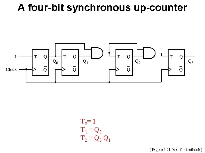
![A four-bit synchronous up-counter [ Figure 5. 21 from the textbook ] A four-bit synchronous up-counter [ Figure 5. 21 from the textbook ]](https://slidetodoc.com/presentation_image/5d4a5c0b3005f472033300b0fb668377/image-33.jpg)

![A four-bit counter with D flip-flops [ Figure 5. 23 from the textbook ] A four-bit counter with D flip-flops [ Figure 5. 23 from the textbook ]](https://slidetodoc.com/presentation_image/5d4a5c0b3005f472033300b0fb668377/image-45.jpg)

![A counter with parallel-load capability [ Figure 5. 24 from the textbook ] A counter with parallel-load capability [ Figure 5. 24 from the textbook ]](https://slidetodoc.com/presentation_image/5d4a5c0b3005f472033300b0fb668377/image-47.jpg)
![What does this circuit do? [ Figure 5. 25 a from the textbook ] What does this circuit do? [ Figure 5. 25 a from the textbook ]](https://slidetodoc.com/presentation_image/5d4a5c0b3005f472033300b0fb668377/image-51.jpg)


- Slides: 56

Cpr. E 281: Digital Logic Instructor: Alexander Stoytchev http: //www. ece. iastate. edu/~alexs/classes/

Registers & Counters Cpr. E 281: Digital Logic Iowa State University, Ames, IA Copyright © Alexander Stoytchev

Administrative Stuff • The second midterm is next week. • No homework is due next week. • You’ll still have labs though

Administrative Stuff • Midterm Exam #2 • When: Monday March 31. • Where: This classroom • What: Chapters 1, 2, 3, 4 and 5. 1 -5. 7 • The exam will be open book and open notes (you can bring up to 3 pages of handwritten notes).

Midterm 2: Format • The exam will be out of 130 points • You need 95 points to get an A • It will be great if you can score more than 100 points. § but you can’t roll over your extra points

Midterm 2: Topics • • Binary Numbers and Hexadecimal Numbers 1’s complement and 2’s complement representation Addition and subtraction of binary numbers Circuits for adders and fast adders • Single and Double precision IEEE floating point formats • Converting a real number to the IEEE format • Converting a floating point number to base 10 • Multiplexers (circuits and function) • Synthesis of logic functions using multiplexers • Shannon’s Expansion Theorem

Midterm 2: Topics • • • Decoders (circuits and function) Demultiplexers Encoders (binary and priority) Code Converters K-maps for 2, 3, and 4 variables • Synthesis of logic circuits using adders, multiplexers, encoders, decoders, and basic logic gates • Synthesis of logic circuits given constraints on the available building blocks that you can use • Latches (circuits, behavior, timing diagrams) • Flip-Flops (circuits, behavior, timing diagrams)

Registers

Register (Definition) An n-bit structure consisting of flip-flops

Parallel-Access Register

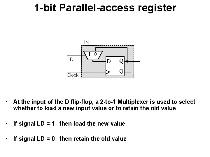
1 -bit Parallel-access register IN LD Clock 1 0 D Q Q • At the input of the D flip-flop, a 2 -to-1 Multiplexer is used to select whether to load a new input value or to retain the old value • If signal LD = 1 then load the new value • If signal LD = 0 then retain the old value

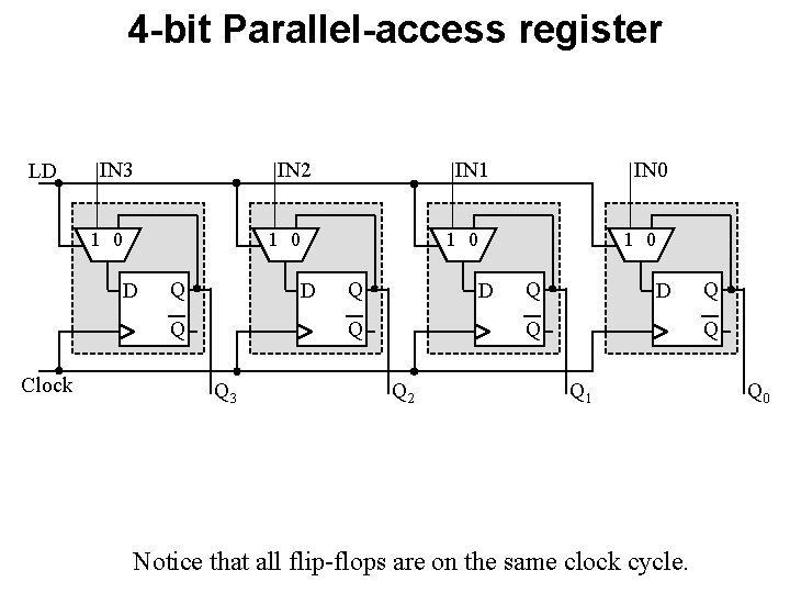
4 -bit Parallel-access register LD IN 3 IN 2 1 0 D Q Q 3 IN 0 1 0 D Q Clock IN 1 Q D Q Q 2 Q Q Q 1 Notice that all flip-flops are on the same clock cycle. Q 0

Shift Register

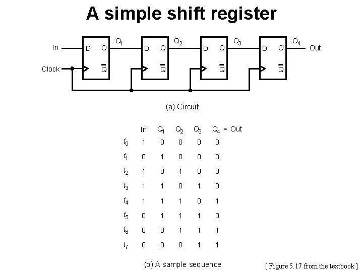
A simple shift register In Clock D Q Q 1 D Q Q Q 2 D Q Q Q 3 Q D Q Q 4 Out Q (a) Circuit In Q 1 Q 2 Q 3 Q 4 = Out t 0 1 0 0 t 1 0 0 0 t 2 1 0 0 t 3 1 1 0 t 4 1 1 1 0 1 t 5 0 1 1 1 0 t 6 0 0 1 1 1 t 7 0 0 0 1 1 (b) A sample sequence [ Figure 5. 17 from the textbook ]

Parallel-Access Shift Register
![Parallelaccess shift register Figure 5 18 from the textbook Parallel-access shift register [ Figure 5. 18 from the textbook ]](https://slidetodoc.com/presentation_image/5d4a5c0b3005f472033300b0fb668377/image-16.jpg)
Parallel-access shift register [ Figure 5. 18 from the textbook ]

Register File

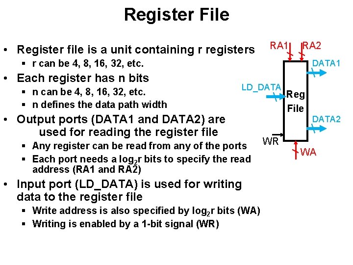
Register File • Register file is a unit containing r registers RA 1 RA 2 § r can be 4, 8, 16, 32, etc. • Each register has n bits § n can be 4, 8, 16, 32, etc. § n defines the data path width DATA 1 LD_DATA • Output ports (DATA 1 and DATA 2) are used for reading the register file § Any register can be read from any of the ports § Each port needs a log 2 r bits to specify the read address (RA 1 and RA 2) • Input port (LD_DATA) is used for writing data to the register file § Write address is also specified by log 2 r bits (WA) § Writing is enabled by a 1 -bit signal (WR) Reg File DATA 2 WR WA

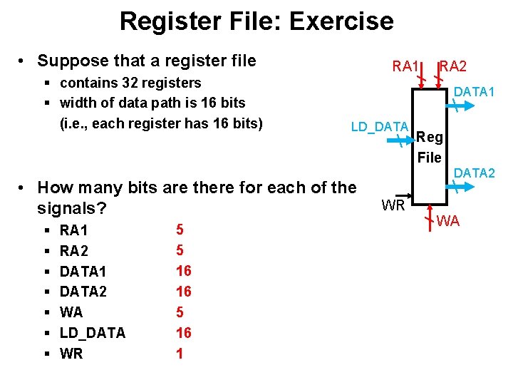
Register File: Exercise • Suppose that a register file § contains 32 registers § width of data path is 16 bits (i. e. , each register has 16 bits) RA 1 DATA 1 LD_DATA • How many bits are there for each of the signals? § § § § RA 1 RA 2 DATA 1 DATA 2 WA LD_DATA WR 5 5 16 16 5 16 1 RA 2 Reg File DATA 2 WR WA

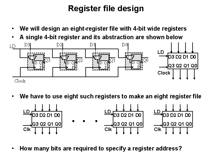
Register file design • We will design an eight-register file with 4 -bit wide registers • A single 4 -bit register and its abstraction are shown below LD D 3 D 2 D 1 D 0 LD 1 0 D Q P Q 3 1 0 D Q P Q 2 1 0 D Q P Q 1 1 0 D Q P Q 0 D 3 D 2 D 1 D 0 Q 3 Q 2 Q 1 Q 0 Clock • We have to use eight such registers to make an eight register file LD D 3 D 2 D 1 D 0 LD Q 3 Q 2 Q 1 Q 0 Clk D 3 D 2 D 1 D 0 Q 3 Q 2 Q 1 Q 0 Clk • How many bits are required to specify a register address?

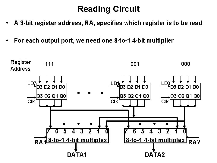
Reading Circuit • A 3 -bit register address, RA, specifies which register is to be read • For each output port, we need one 8 -to-1 4 -bit multiplier Register Address 111 000 LD 7 D 3 D 2 D 1 D 0 LD 1 D 3 D 2 D 1 D 0 LD 0 D 3 D 2 D 1 D 0 Q 3 Q 2 Q 1 Q 0 Clk 7 6 5 4 3 2 1 0 RA 1 8 -to-1 4 -bit multiplex DATA 1 Clk 7 6 5 4 3 2 1 0 8 -to-1 4 -bit multiplex RA 2 DATA 2

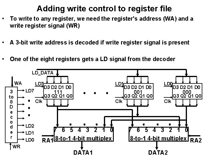
Adding write control to register file • To write to any register, we need the register's address (WA) and a write register signal (WR) • A 3 -bit write address is decoded if write register signal is present • One of the eight registers gets a LD signal from the decoder LD_DATA WA 3 to 8 D e c o d e r LD 7 D 3 D 2 D 1 D 0 LD 1 D 3 D 2 D 1 D 0 LD 0 D 3 D 2 D 1 D 0 Q 3 Q 2 Q 1 Q 0 111 001 Clk LD 2 LD 1 LD 0 Clk 7 6 5 4 3 2 1 0 RA 1 8 -to-1 4 -bit multiplex 000 Clk 7 6 5 4 3 2 1 0 8 -to-1 4 -bit multiplex RA 2 WR DATA 1 DATA 2

Counters
![A threebit upcounter Figure 5 19 from the textbook A three-bit up-counter [ Figure 5. 19 from the textbook ]](https://slidetodoc.com/presentation_image/5d4a5c0b3005f472033300b0fb668377/image-24.jpg)
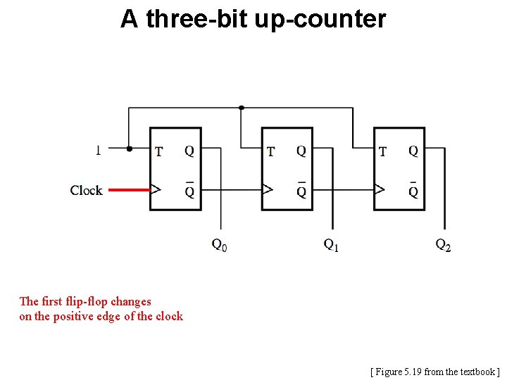
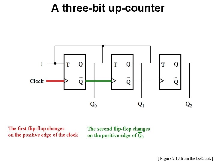
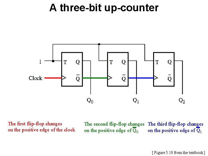
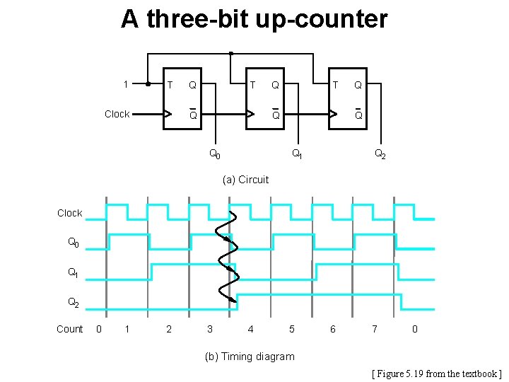
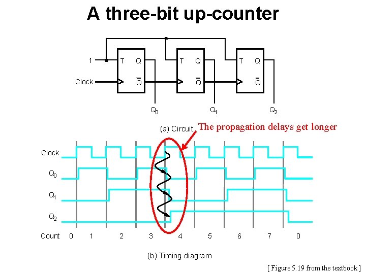
A three-bit up-counter [ Figure 5. 19 from the textbook ]

A three-bit up-counter The first flip-flop changes on the positive edge of the clock [ Figure 5. 19 from the textbook ]

A three-bit up-counter The first flip-flop changes on the positive edge of the clock The second flip-flop changes on the positive edge of Q 0 [ Figure 5. 19 from the textbook ]

A three-bit up-counter The first flip-flop changes on the positive edge of the clock The second flip-flop changes The third flip-flop changes on the positive edge of Q 0 on the positive edge of Q 1 [ Figure 5. 19 from the textbook ]

A three-bit up-counter 1 T Clock Q T Q Q 0 Q Q Q 1 Q 2 (a) Circuit Clock Q 0 Q 1 Q 2 Count 0 1 2 3 4 5 6 7 0 (b) Timing diagram [ Figure 5. 19 from the textbook ]

A three-bit up-counter 1 T Clock Q T Q Q 0 Q Q 1 (a) Circuit Q Q 2 The propagation delays get longer Clock Q 0 Q 1 Q 2 Count 0 1 2 3 4 5 6 7 0 (b) Timing diagram [ Figure 5. 19 from the textbook ]
![A threebit downcounter Figure 5 20 from the textbook A three-bit down-counter [ Figure 5. 20 from the textbook ]](https://slidetodoc.com/presentation_image/5d4a5c0b3005f472033300b0fb668377/image-30.jpg)
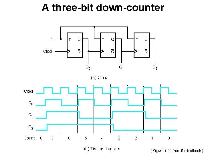
A three-bit down-counter [ Figure 5. 20 from the textbook ]

A three-bit down-counter 1 T Clock Q T Q Q 0 Q Q Q 1 Q 2 (a) Circuit Clock Q 0 Q 1 Q 2 Count 0 7 6 5 4 3 (b) Timing diagram 2 1 0 [ Figure 5. 20 from the textbook ]

Synchronous Counters
![A fourbit synchronous upcounter Figure 5 21 from the textbook A four-bit synchronous up-counter [ Figure 5. 21 from the textbook ]](https://slidetodoc.com/presentation_image/5d4a5c0b3005f472033300b0fb668377/image-33.jpg)
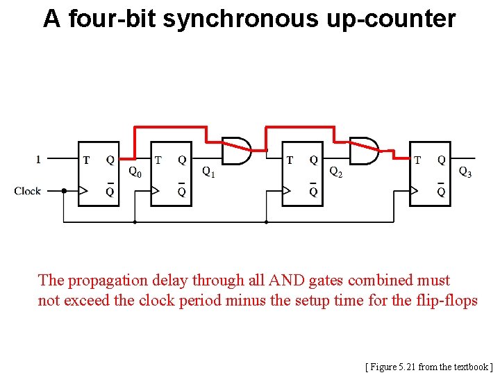
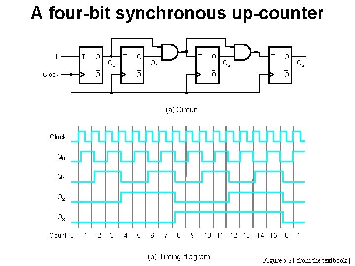
A four-bit synchronous up-counter [ Figure 5. 21 from the textbook ]

A four-bit synchronous up-counter The propagation delay through all AND gates combined must not exceed the clock period minus the setup time for the flip-flops [ Figure 5. 21 from the textbook ]

A four-bit synchronous up-counter 1 T Clock Q Q 0 T Q Q Q T Q 1 Q Q 2 T Q Q Q 3 Q (a) Circuit Clock Q 0 Q 1 Q 2 Q 3 Count 0 1 2 3 4 5 6 7 8 9 10 11 12 13 (b) Timing diagram 14 15 0 1 [ Figure 5. 21 from the textbook ]

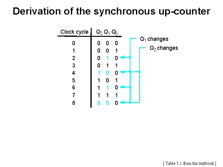
Derivation of the synchronous up-counter Clock cycle 0 1 2 3 4 5 6 7 8 Q 2 Q 1 Q 0 0 0 1 1 0 0 1 0 1 0 Q 1 changes Q 2 changes [ Table 5. 1 from the textbook ]

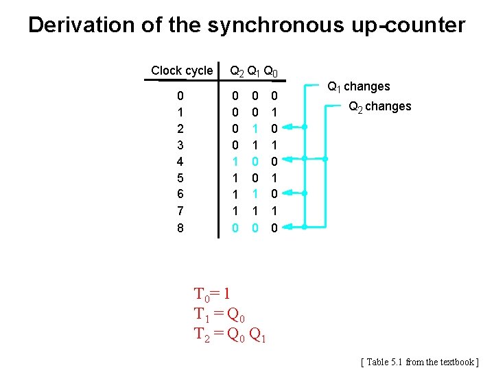
Derivation of the synchronous up-counter Clock cycle 0 1 2 3 4 5 6 7 8 Q 2 Q 1 Q 0 0 0 1 1 0 0 1 0 1 0 Q 1 changes Q 2 changes T 0= 1 T 1 = Q 0 T 2 = Q 0 Q 1 [ Table 5. 1 from the textbook ]

A four-bit synchronous up-counter T 0= 1 T 1 = Q 0 T 2 = Q 0 Q 1 [ Figure 5. 21 from the textbook ]

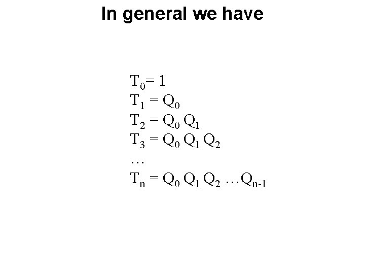
In general we have T 0= 1 T 1 = Q 0 T 2 = Q 0 Q 1 T 3 = Q 0 Q 1 Q 2 … Tn = Q 0 Q 1 Q 2 …Qn-1

Adding Enable and Clear Capability

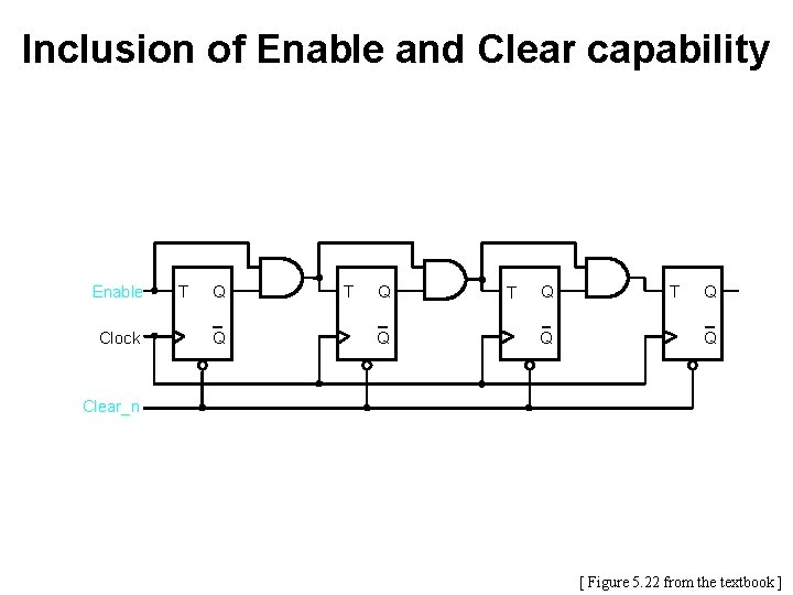
Inclusion of Enable and Clear capability Enable Clock T Q Q Clear_n [ Figure 5. 22 from the textbook ]

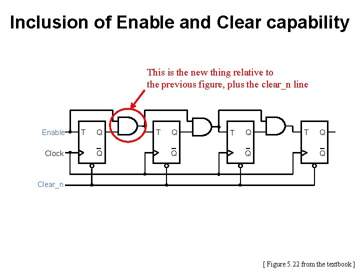
Inclusion of Enable and Clear capability This is the new thing relative to the previous figure, plus the clear_n line Enable Clock T Q Q Clear_n [ Figure 5. 22 from the textbook ]

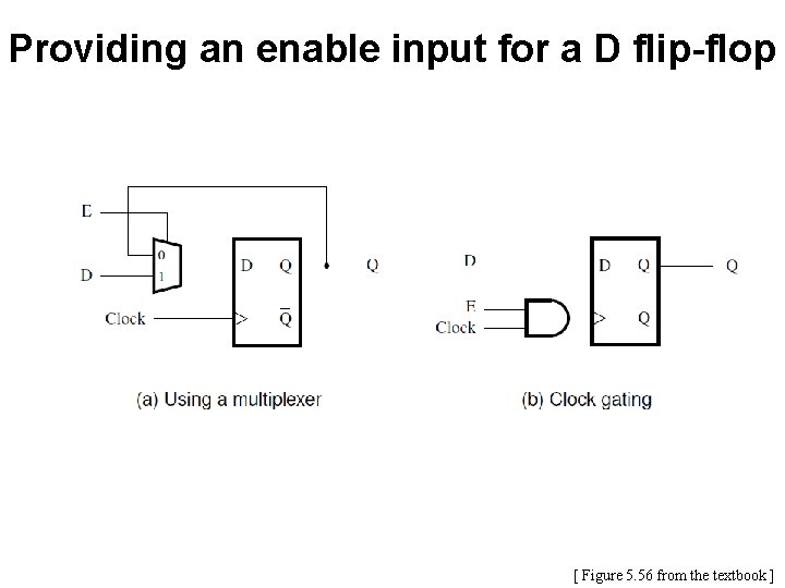
Providing an enable input for a D flip-flop [ Figure 5. 56 from the textbook ]

Synchronous Counter with D Flip-Flops
![A fourbit counter with D flipflops Figure 5 23 from the textbook A four-bit counter with D flip-flops [ Figure 5. 23 from the textbook ]](https://slidetodoc.com/presentation_image/5d4a5c0b3005f472033300b0fb668377/image-45.jpg)
A four-bit counter with D flip-flops [ Figure 5. 23 from the textbook ]

Counters with Parallel Load
![A counter with parallelload capability Figure 5 24 from the textbook A counter with parallel-load capability [ Figure 5. 24 from the textbook ]](https://slidetodoc.com/presentation_image/5d4a5c0b3005f472033300b0fb668377/image-47.jpg)
A counter with parallel-load capability [ Figure 5. 24 from the textbook ]

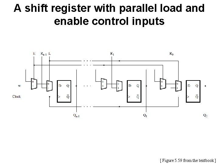
A shift register with parallel load and enable control inputs [ Figure 5. 59 from the textbook ]

Reset Synchronization

Motivation • An n-bit counter counts from 0, 1, …, 2 n-1 • For example a 3 -bit counter counts up as follow § 0, 1, 2, 3, 4, 5, 6, 7, 0, 1, 2, … • What if we want it to count like this § 0, 1, 2, 3, 4, 5, 0, 1, … • In other words, what is the cycle is not a power of 2?
![What does this circuit do Figure 5 25 a from the textbook What does this circuit do? [ Figure 5. 25 a from the textbook ]](https://slidetodoc.com/presentation_image/5d4a5c0b3005f472033300b0fb668377/image-51.jpg)
What does this circuit do? [ Figure 5. 25 a from the textbook ]

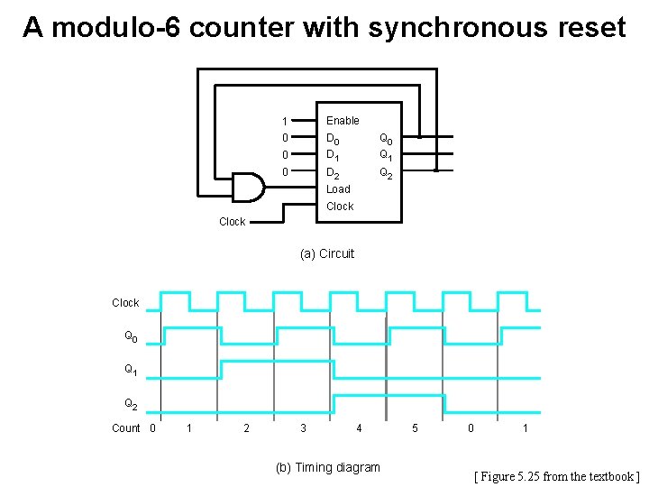
A modulo-6 counter with synchronous reset 1 Enable 0 D 0 Q 0 0 D 1 Q 1 0 D 2 Q 2 Load Clock (a) Circuit Clock Q 0 Q 1 Q 2 Count 0 1 2 3 4 (b) Timing diagram 5 0 1 [ Figure 5. 25 from the textbook ]

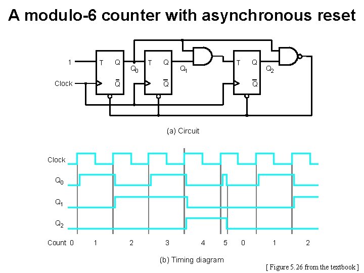
A modulo-6 counter with asynchronous reset 1 T Clock Q Q 0 Q T Q 1 Q Q 2 Q (a) Circuit Clock Q 0 Q 1 Q 2 Count 0 1 2 3 4 (b) Timing diagram 5 0 1 2 [ Figure 5. 26 from the textbook ]

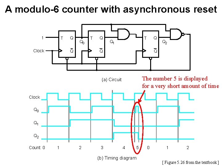
A modulo-6 counter with asynchronous reset 1 T Clock Q Q 0 Q T Q 1 Q Q 2 Q The number 5 is displayed for a very short amount of time (a) Circuit Clock Q 0 Q 1 Q 2 Count 0 1 2 3 4 (b) Timing diagram 5 0 1 2 [ Figure 5. 26 from the textbook ]

Questions?

THE END