UNIT II IO Interfacing I Contents Interfacing of


 is a two-lead semiconductor light source. It")


 Function Set: 8 -bit")
 Clear display screen 0 x 01 Return")
 Force cursor to beginning of 1 st")


 is high, the • LCD is busy")
 • ADCs (analog-to-digital converters) most widely used devices for")


 Select an analog channel by providing bits to A,")


 To see if any key is pressed, the columns are scanned over and")
 To detect which row key press belongs to, it grounds one row at")
 To identify the key press, it rotates the column bits, one bit at")


 www. wikinote. org 2) Muhammad Ali Mazidi, Janice Gillispie Mazidi, Rolin D.")
- Slides: 71
UNIT II IO Interfacing - I
Contents • Interfacing of: LEDS, Keypad, 7 -segment multiplexed display, LCD, ADC 0809 (All programs in assembly). • Programming environment: Study of software development tool chain (IDE), hardware debugging tools (timing analysis using logic analyser)
LED Interfacing • A light-emitting diode (LED) is a two-lead semiconductor light source. It is a p–n junction diode that emits light when activated.
• An LED can be interfaced with 8051 for various purpose. • The Port Pins are configured in the output direction. So, once the Logic "1" is the at O/P pin, then an LED will be turned "ON". And when Logic "0" is given the LED will be turned "OFF". • Simply: Logic "1" -> 5 V DC to output pin Logic "0" -> 0 V to output pin. • LED with common cathode mode can be connected with 8051 along with a resistor. • Thus, using the current limiting resistor, the LED will blink according to the written program in 8051.
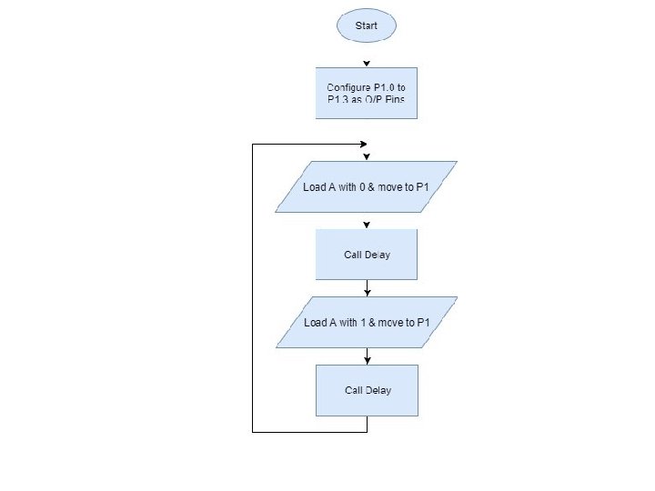
• Write a Assembly program to Blink 4 LED's continuously which are connected to Port P 1.
ORG 0000 H MOV A, #0 FH LOOP: MOV P 1, A ACALL DELAY SJMP LOOP DELAY: MOV R 0, #05 H HERE 1: MOV R 1, #02 H HERE: DJNZ R 1, HERE DJNZ R 0, HERE 1 RET END
LCD • LCD is finding widespread use replacing LEDs Ø The declining prices of LCD. ØThe ability to display numbers, characters, and graphics. ØIncorporation of a refreshing controller into the LCD, thereby relieving the CPU of the task of refreshing the LCD. ØEase of programming for characters and graphics.
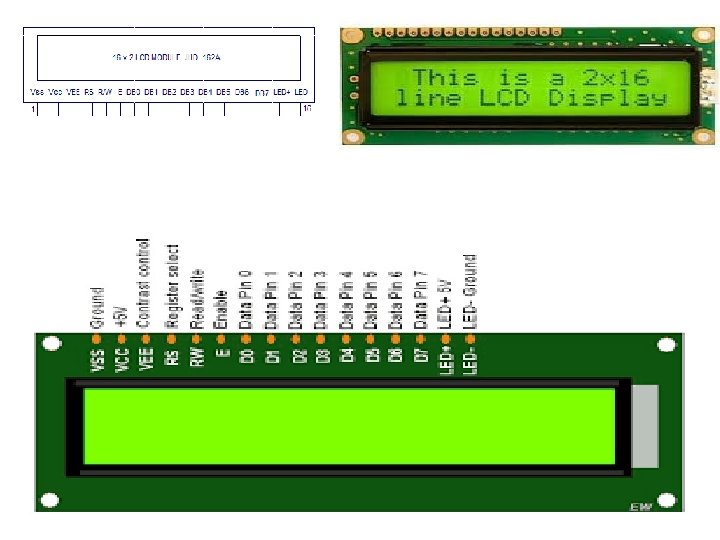
Pin Descriptions for LCD Pin Symbol I/O Description 1 VSS - Ground 2 VCC - +5 V power supply 3 VEE - Power supply to control contrast 4 RS I RS=0 to select command register, RS=1 to select data register 5 R/W I R/W=0 for write, R/W=1 for read 6 E I/O Enable (used by the LCD to latch information presented to its data bus) 7 DB 0 I/O 8 -bit Data bus 8 DB 1 I/O 8 -bit Data bus 9 DB 2 I/O 8 -bit Data bus 10 DB 3 I/O 8 -bit Data bus 11 DB 4 I/O 8 -bit Data bus 12 DB 5 I/O 8 -bit Data bus 13 DB 6 I/O 8 -bit Data bus -Send displayed information or instruction command codes to the LCD - Read the contents of the LCD’s internal registers
• RS, Register Select: Ø Two major registers inside the LCD. Ø RS pin is used for their selection. Ø If RS=0, Instruction command code register is selected, allowing the user to send command such as clear display, cursor at home etc. Ø If RS=1, Data register is selected, allowing the user to send data to be displayed on the LCD.
• R/W, Read/Write: Ø R/W input allows the user to write information to the LCD or read information from it. Ø R/W= 1, When Reading Ø R/W=0, When Writing
• E, Enable: Ø Used to latch information presented to its data pins. Ø When data is supplied to data pins, a high-tolow pulse must be applied to this in order for the LCD to latch in data present at the data pins. Ø This pulse must be a minimum of 450 ns wide.
• D 0 -D 7: Ø D 0 -D 7 are used to send information to the LCD or read the contents of the LCD’s internal registers. Ø E. g. Ø To display letters and numbers, send ASCII codes for the letters A-Z, a-z and numbers 0 -9 to these pins making RS=1. Ø Instruction command codes can also be sent to the LCD. Ø Rs=0 is used to check the busy flag bit to see if the LCD is ready to receive information.
Ø Busy flag is D 7 and can be read when R/W=1 and RS=0. Ø When D 7=1(busy flag=1), LCD is busy in internal operations and will not accept any new information. Ø When D 7=0, LCD is ready to receive new information. Ø NOTE: Busy flag should be checked before writing any data to the LCD.
LCD Command Codes Command to LCD Instruction Register Code (Hex) Function Set: 8 -bit mode, 1 Line, 5 x 7 Dots matrix for each character display 0 x 30 Function Set: 8 -bit mode, 2 Line, 5 x 7 Dots matrix for each character display 0 x 38 Function Set: 4 -bit mode, 1 Line, 5 x 7 Dots matrix for each character display 0 x 20 Function Set: 4 -bit mode, 2 Line, 5 x 7 Dots matrix for each character display 0 x 28 Clear display screen 0 x 01 Return Home 0 x 02
Command to LCD Instruction Register Code (Hex) Clear display screen 0 x 01 Return Home 0 x 02 Decrement cursor(Shift to left) 0 x 04 Increment cursor(Shift to Right) 0 x 06 Display off Cursor off 0 x 08 Display on Cursor on 0 x 0 E Display on Cursor off 0 x 0 C Display on Cursor blinking 0 x 0 F Shift entire display left 0 x 18 Shift entire display right 0 x 1 C Move cursor left by one character 0 x 10 Move cursor right by one character 0 x 14
Command to LCD Instruction Register Code (Hex) Force cursor to beginning of 1 st line 0 x 80 Force cursor to beginning of 2 nd line 0 x. C 0 2 lines and 5*7 matrix 0 x 38 Shift display right 0 x 05 Shift display left 0 x 07 Display off , cursor on 0 x 0 A Shift the entire display to the left 0 x 18
• Sending Data to LCD without checking busy flag: • To send any of the commands to the LCD, make pin RS=0. For data, make RS=1. Then send a high-to-low pulse to the E pin to enable the internal latch of the LCD. Ø ; calls a time delay before sending next data/command Ø ; P 1. 0 -P 1. 7 are connected to LCD data pins D 0 -D 7 Ø ; P 2. 0 is connected to RS pin of LCD Ø ; P 2. 1 is connected to R/W pin of LCD Ø ; P 2. 2 is connected to E pin of LCD
ORG 0000 H MOV A, #38 H ; ACALL COMNWRT ; ACALL DELAY ; MOV A, #0 EH ; ACALL COMNWRT ; ACALL DELAY ; MOV A, #01 ; ACALL COMNWRT ; ACALL DELAY ; MOV A, #06 H ; ACALL COMNWRT ; ACALL DELAY ; MOV A, #84 H ; ACALL COMNWRT ; ACALL DELAY ; INIT. LCD 2 LINES, 5 X 7 MATRIX call command subroutine give LCD some time display on, cursor on call command subroutine give LCD some time clear LCD call command subroutine give LCD some time shift cursor right call command subroutine give LCD some time cursor at line 1, pos. 4 call command subroutine give LCD some time
MOV A, #’N’ ; ACALL DATAWRT ; ACALL DELAY ; MOV A, #’O’ ; ACALL DATAWRT ; AGAIN: SJMP AGAIN ; display letter N call display subroutine give LCD some time display letter O call display subroutine stay here COMNWRT: ; MOV P 1, A ; CLR P 2. 0 ; CLR P 2. 1 ; SETB P 2. 2 ; CLR P 2. 2 ; RET send command to LCD copy reg A to port 1 RS=0 for command R/W=0 for write E=1 for high pulse E=0 for H-to-L pulse
DATAWRT: ; MOV P 1, A ; CLR P 2. 0 ; CLR P 2. 1 ; SETB P 2. 2 ; CLR P 2. 2 ; RET write data to LCD copy reg A to port 1 RS=0 for command R/W=0 for write E=1 for high pulse E=0 for H-to-L pulse
DELAY: MOV R 3, #50 ; 50 or higher for fast CPUs HERE 2: MOV R 4, #255 ; R 4 = 255 HERE: DJNZ R 4, HERE ; stay until R 4 becomes 0 DJNZ R 3, HERE 2 RET END
• Sending Data to LCD with checking busy flag: Ø While sending data to LCD without checking busy flag, long delay should be provided between issuing data or commands to LCD. Ø Its better to monitor the busy flag before issuing a command or data to the LCD. Ø Enable should be applied a pulse from High to Low while Writing the data and Low to High while Reading the data.
Check busy flag before sending data, command to LCD P 1=data pin P 2. 0 connected to RS pin P 2. 1 connected to R/W pin P 2. 2 connected to E pin ORG 0000 H MOV A, #38 H ; ACALL COMMAND ; MOV A, #0 EH ; ACALL COMMAND ; init. LCD 2 lines , 5 x 7 matrix issue command LCD on, cursor on issue command
MOV A, #01 H ; ACALL COMMAND ; MOV A, #06 H ; ACALL COMMAND ; MOV A, #86 H ; ACALL COMMAND ; MOV A, #’N’ ; ACALL DATA_DISPLAY MOV A, #’O’ ; ACALL DATA_DISPLAY HERE: SJMP HERE ; clear LCD command issue command shift cursor right issue command cursor: line 1, pos. 6 command subroutine display letter N display letter O STAY HERE
COMMAND: ACALL READY ; MOV P 1, A ; CLR P 2. 0 ; CLR P 2. 1 ; SETB P 2. 2 ; CLR P 2. 2 ; RET is LCD ready? issue command code RS=0 for command R/W=0 to write to LCD E=1 for H-to-L pulse E=0, latch in
DATA_DISPLAY: ACALL READY ; MOV P 1, A ; SETB P 2. 0 ; CLR P 2. 1 ; SETB P 2. 2 ; CLR P 2. 2 ; RET is LCD ready? issue data RS=1 for data R/W =0 to write to LCD E=1 for H-to-L pulse E=0, latch in
READY: SETB P 1. 7 ; make P 1. 7 input port CLR P 2. 0 ; RS=0 access command reg SETB P 2. 1 ; R/W=1 read command reg ; read command reg and check busy flag BACK: CLR P 2. 2 ; E=0 L-to-H pulse ACALL DELAY SETB P 2. 2 ; E=1 for L-to-H pulse JB P 1. 7, BACK ; Stay until busy flag=0 RET END To read the command register, we make R/W=1, RS=0, and a L-to-H pulse for the E pin. If bit 7 (busy flag) is high, the LCD is busy and no information should be issued to it.
• If bit 7 (busy flag) is high, the • LCD is busy and no information • should be issued to it.
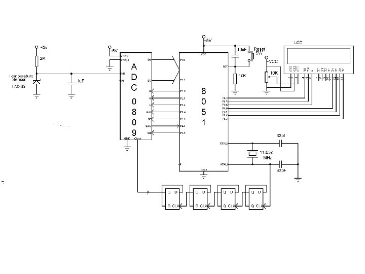
Analog To Digital Converter (ADC) • ADCs (analog-to-digital converters) most widely used devices for data acquisition Ø A physical quantity, like temperature, pressure, humidity, and velocity, etc. , is converted to electrical (voltage, current) signals using a device called a transducer, or sensor Ø We need an analog-to-digital converter to translate the analog signals to digital numbers, so microcontroller can read them
ADC 808/0809 • 8 analog inputs • 8 -bit data output • It allows us to monitor up to 8 different transducers using only a single chip • The 8 analog input channels are multiplexed and selected according to table below using three address pins, A, B, and C
Selected Analog Channel IN 7 C B A IN 0 0 IN 1 0 0 1 IN 2 0 1 0 IN 3 0 1 1 IN 4 1 0 0 IN 5 1 0 1 IN 6 1 1 0 IN 7 1 1 1
Steps for ADC Programming 1) Select an analog channel by providing bits to A, B, and C addresses. 2) Activate the ALE pin. Ø It needs an L-to-H pulse to latch in the address. 3) Activate SC (start conversion ) by an H-to-L pulse to initiate conversion. 4) Monitor EOC (end of conversion) to see whether conversion is finished. 5) Activate OE (output enable ) to read data out of the ADC chip. Ø An H-to-L pulse to the OE pin will bring digital data out of the chip.
ORG 00 h ALE BIT P 2. 6 OE BIT P 2. 5 SOC BIT P 2. 6 EOC BIT P 2. 7 ADDR_A BIT P 2. 0 ADDR_B BIT P 2. 1 ADDR_C BIT P 2. 2 MYDATA EQU P 1 ORG 00 H MOV MYDATA, #0 FFH SETB EOC CLR ALE CLR SOC CLR OE BACK: CLR ADDR_C CLR ADDR_B CLR ADDR_A ACALL DELAY SETB ALE ACALL DELAY SETB SOC ACALL DELAY CLR ALE CLR SOC HERE: JB EOC, HERE 1: JNB EOC, HERE 1 SETB OE ACALL DELAY MOV A, MYDATA CLR OE ACALL CONVERSION ACALL DISPLAY SJMP BACK
Interfacing of Keypad with 8051 • 4*4 Keypad Interfacing : Keypad is used as an input device to read the key pressed by user and to process it. 4 x 4 keypad consists of 4 rows and 4 columns. Switches are placed between the rows and columns. A key press establishes a connection between corresponding row and column between which the switch is placed.
Keyboard Interfacing • Keyboards are organized in a matrix of rows and columns Ø The CPU accesses both rows and columns through ports. Ø Therefore, with two 8 -bit ports, an 8 x 8 matrix of keys can be connected to a microprocessor. • When a key is pressed, a row and a column make a contact. Otherwise, there is no connection between rows and columns.
• A 4 x 4 matrix connected to two ports : The rows are connected to an output port and the columns are connected to an input port.
• To detect a pressed key, Ø The microcontroller grounds all rows by providing 0 to the output latch, then it reads the columns. Ø If the data read from columns is D 3 – D 0 = 1111, no key has been pressed and the process continues till key press is detected. Ø If one of the column bits has a zero, this means that a key press has occurred. Ø For example, if D 3 – D 0 = 1101, this means that a key in the D 1 column has been pressed. Ø After detecting a key press, microcontroller will go through the process of identifying the key.
• Starting with the top row, the microcontroller grounds it by providing a low to row D 0 only. Ø It reads the columns, if the data read is all 1 s, no key in that row is activated and the process is moved to the next row. • It grounds the next row, reads the columns, and checks for any zero. Ø This process continues until the row is identified. • After identification of the row in which the key has been pressed. Ø Find out which column the pressed key belongs to.
• Program for detection and identification of key activation goes through the following stages: 1) To make sure that the preceding key has been released, 0 s are output to all rows at once, and the columns are read and checked repeatedly until all the columns are high • When all columns are found to be high, the program waits for a short amount of time before it goes to the next stage of waiting for a key to be pressed.
2) To see if any key is pressed, the columns are scanned over and over in an infinite loop until one of them has a 0 on it. • Remember that the output latches connected to rows still have their initial zeros (provided in stage 1), making them grounded. • After the key press detection, it waits 20 ms for the bounce and then scans the columns again. (a) it ensures that the first key press detection was not an erroneous one due a spike noise. (b) the key press. If after the 20 -ms delay the key is still pressed, it goes back into the loop to detect a real key press.
3) To detect which row key press belongs to, it grounds one row at a time, reading the columns each time • If it finds that all columns are high, this means that the key press cannot belong to that row – Therefore, it grounds the next row and continues until it finds the row the key press belongs to • Upon finding the row that the key press belongs to, it sets up the starting address for the look-up table holding the scan codes (or ASCII) for that row
4) To identify the key press, it rotates the column bits, one bit at a time, into the carry flag and checks to see if it is low • Upon finding the zero, it pulls out the ASCII code for that key from the look-up table. • otherwise, it increments the pointer to point to the next element of the look-up table.
Flowchart for detection and identification of key
Keyboard Program ; keyboard subroutine. This program sends the ASCII ; code for pressed key to P 0. 1 ; P 1. 0 -P 1. 3 connected to rows, P 2. 0 -P 2. 3 to column MOV P 2, #0 FFH ; make P 2 an input port K 1: MOV P 1, #0 ; ground all rows at once MOV A, P 2 ; read all col. (ensure keys open) ANL A, 00001111 B ; masked unused bits CJNE A, #00001111 B, K 1 ; till all keys release
K 2: ACALL DELAY ; call 20 msec delay MOV A, P 2 ; see if any key is pressed ANL A, 00001111 B ; mask unused bits CJNE A, #00001111 B, OVER; key pressed, find row SJMP K 2 ; check till key pressed OVER: ACALL DELAY ; wait 20 msec debounce time MOV A, P 2 ; check key closure ANL A, 00001111 B ; mask unused bits CJNE A, #00001111 B, OVER 1; key pressed, find ; row SJMP K 2 ; if none, keep polling
OVER 1: MOV P 1, #11111110 B ; ground row 0 MOV A, P 2 ; read all columns ANL A, #00001111 B ; mask unused bits CJNE A, #00001111 B, ROW_0 ; key row 0, ; find col. MOV P 1, #11111101 B ; ground row 1 MOV A, P 2 ; read all columns ANL A, #00001111 B ; mask unused bits CJNE A, #00001111 B, ROW_1 ; key row 1, find ; col. MOV P 1, #11111011 B ; ground row 2 MOV A, P 2 ; read all columns
ANL A, #00001111 B ; mask unused bits CJNE A, #00001111 B, ROW_2 ; key row 2, find col. MOV P 1, #11110111 B ; ground row 3 MOV A, P 2 ; read all columns ANL A, #00001111 B ; mask unused bits CJNE A, #00001111 B, ROW_3 ; key row 3, find col. LJMP K 2 ; if none, false ; input, repeat ROW_0: MOV DPTR, #KCODE 0 ; set DPTR=start of row 0 SJMP FIND ; find col. Key belongs to ROW_1: MOV DPTR, #KCODE 1 ; set DPTR=start of ; row SJMP FIND ; find col. Key belongs to
ROW_2: MOV DPTR, #KCODE 2 ; set DPTR=start of row 2 SJMP FIND ; find col. Key belongs to ROW_3: MOV DPTR, #KCODE 3 ; set DPTR=start of row 3 FIND: RRC A ; see if any CY bit low JNC MATCH ; if zero, get ASCII code INC DPTR ; point to next col. addr SJMP FIND ; keep searching MATCH: CLR A ; set A=0 (match is found) MOVC A, @A+DPTR ; get ASCII from table MOV P 0, A ; display pressed key LJMP K 1
; ASCII LOOK-UP TABLE FOR EACH ROW ORG 300 H KCODE 0: DB ‘ 0’, ’ 1’, ’ 2’, ’ 3’ ; ROW 0 KCODE 1: DB ‘ 4’, ’ 5’, ’ 6’, ’ 7’ ; ROW 1 KCODE 2: DB ‘ 8’, ’ 9’, ’A’, ’B’ ; ROW 2 KCODE 3: DB ‘C’, ’D’, ’E’, ’F’ ; ROW 3 END
Software IDE To develop an assembly language program we need certain program development tools. An assembly language program consists of Mnemonics which are nothing but short abbreviated English instructions given to the controller. The various development tools required for Microcontroller programming are explained below.
Editor An Editor is a program which allows us to create a file containing the assembly language statements for the program. Examples of some editors are PC write Wordstar. As we type the program the editor stores the ACSII codes for the letters and numbers in successive RAM locations. If any typing mistake is done editor will alert us to correct it. If we leave out a program statement an editor will let you move everything down and insert a line.
• After typing all the program we have to save the program. This we call it as source file. The next step is to process the source file with an assembler.
Assembler An Assembler is used to translate the assembly language mnemonics into machine language( i. e binary codes). When you run the assembler it reads the source file of your program from where you have saved it. The assembler generates a file with the extension. hex. This file consists of hexadecimal values encoding a sequence of data and their starting offset or absolute address.
Compiler A compiler is a program which converts the high level language program like “C” into binary or machine code. Using high level languages it is easy to manage complex data structures which are often required for data manipulation. Because of its ease , flexibility and debug options now a days the compilers have become very popular in the market. Compilers like Keil , Ride and IAR workbench are very popular.
Debugger/Simulator A debugger is a program which allows to execute the program, and troubleshoot or debug it. The debugger allows to look into the contents of registers and memory locations after the program runs. We can also change the contents of registers and memory locations and rerun the program. Some debuggers allows to stop the program after each instruction so that you can check or alter memory and register contents. This is called single step debug.
• A debugger also allows to set a breakpoint at any point in the program. If we insert a break point , the debugger will run the program up to the instruction where the breakpoint is put and then stop the execution. • A simulator is a software program which virtually executes the instructions similar to a microcontroller and shows the results. This will help in evaluating the results without committing any errors. By doing so we can detect the possible logic errors
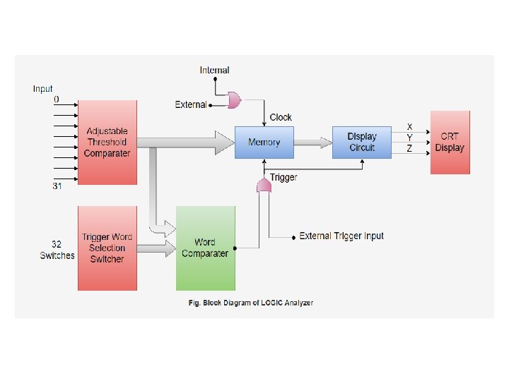
Logic Analyzer • It is separate electronic instrument used to solve both hardware and software problems by simultaneously observing the various signal on screen. • A logical analyzer is basically a multichannel oscilloscope. • Logic analyzer takes input samples and stores it in its own internal memory.
COMPARISON OF OSCILLOSCOPE AND LOGIC ANALYZER OSCILLOSCOPE LOGIC ANALYZER Oscilloscope is used for measuring analogue waveforms: amplitude, phase values, or edge measurements such as rise times, etc. Typical oscilloscope applications: • Investigating waveform shapes, ringing, rise time, etc. • Characterise aspects like waveform jitter and stability. • Measure signal amplitudes. • Detect transients, and unwanted pulses. A logic analyser is used for verifying and debugging the operation of digital designs looking a logic states and timings. Typical logic analyser applications: • Investigate the system operation. • Correlate a large number of digital signals • Detect timing violations • Trace embedded software operation.
Block diagram Explanation • The data on parallel 32 input channels is compared with adjustable threshold voltage to decide the logic level of the input data. • Input data is stored in memory, when trigger occurs data sample stored in memory are displayed on CRT screen. • The trigger can come from external source or from a word comparator block.
• A word comparator block compares input data word which is selected by user through 32 switches • when two word match the word comparator block will trigger the signals
LOGIC analyzer types • Modular Logic Analyzer • It consist of both a chassis or mainframe and logic analyzer modules. The mainframe/chassis contains the display, controls, control computer, and multiple slots into which the actual data-capturing hardware is installed. The modules each have a specific number of channels, and multiple modules may be combined to obtain a very high channel count. While modular logic analyzers are typically more expensive, the ability to combine multiple modules to obtain a high channel count and the generally higher performance of modular logic analyzers often justifies the price. For the very high end modular logic analyzers, the user often must provide their own host PC or purchase an embedded controller compatible with the system.
• Portable Logic Analyzer • It is also referred to as standalone LAs. Portable logic analyzers integrate everything into a single package, with options installed at the factory. While portable logic analyzers generally have lower performance than their modular counterparts, they are often used for general purpose debugging by cost conscious users.
• PC-based Logic Analyzer • The hardware connects to a computer through a USB or Ethernet connection and relays the captured signals to the software on the computer. These devices are typically much smaller and less expensive because they make use of a PC's existing keyboard, display and CPU.
Triggering modes • Triggering from external inputs allows to observe the data smaples at a perticular event to do this user has to program logic analyzer into • Pre-trigger mode • Central trigger mode • Post-trigger mode
Display formats • Provide a time display of logic states: Logic analysers possess a horizontal time axis and a vertical axis to indicate a logic high or low states. In this way a picture of the digital lines can be easily displayed. Multiple channels: Logic analyzers are designed to monitor a large number of digital lines. As logic analyzers are optimised for monitoring a large number of digital circuits, typically they may have anywhere between about 32 and 200+ channels they can monitor, each channel monitoring one digital line. However some specialised logic analyzers are suitably scaled to be able to handle many more lines, and in this way enable tracking and fault finding on much more complex systems.
• Displays logic states: • The vertical display on the analyser displays the logic state as a high of low state. The signals enter the various channels and are converted into a high or low state for further processing within the analyser. It provides a logic timing diagram of the various lines being monitored. • Does NOT display analogue information : • These test instruments do not present any analogue information, and in this way they differ from an oscilloscope. They are purely aimed at monitoring the logic operation of the system. If any analogue information is required, then an oscilloscope must be used in addition.
References 1) www. wikinote. org 2) Muhammad Ali Mazidi, Janice Gillispie Mazidi, Rolin D. Mc. Kinlay, “The 8051 Microncontroller and Embedded Systems”, Second Editin